

Page 1
LMX2354
PLLatinum Fractional N RF/ Integer N IF Dual Low Power
Frequency Synthesizer
LMX2354 2.5 GHz/550 MHz
General Description
The LMX2354 is part of a family of monolithic integrated
fractional N/Integer N frequency synthesizers designed to be
used in a local oscillatorsubsystem for a radio transceiver. It
is fabricated using National’s 0.5 µ ABiC V silicon BiCMOS
process. The LMX2354 contains quadruple modulus prescalers along with modulo 15 or 16 fractional compensation
circuitry in the RF divider. The LMX2354 provides a continuous divide ratio of 80 to 32767 in 16/17/20/21
(1.2 GHz–2.5 GHz) fractional mode and 40 to 16383 in
8/9/12/13 (550 MHz–1.2 GHz) fractional mode. The IF circuitry for the LMX2354 contains an 8/9prescaler, and is fully
programmable. Using a fractional N phase locked loop technique, the LMX2354 can generate very stable low noise
control signals for UHF and VHF voltage controlled oscillators (VCOs).
For the RF PLL, a highly flexible 16 level programmable
charge pump supplies output current magnitudes from 100
µA to 1.6 mA. Two uncommitted CMOS outputs can be used
to provide external control signals, or configured to FastLock
mode. Serial dataistransferredintotheLMX2354 via a three
wire interface (Data, LE, Clock). Supply voltage can range
from 2.7V to 5.5V. The LMX2354 family features very low
current consumption; typically LMX2354 (2.5 GHz) — 7.0
mA. The LMX2354 are available in a 24-pin TSSOP surface
mount plastic package and 24-pin CSP.
Features
n Pin compatible/functional equivalent to the LMX2350
n Enhanced Low Noise Fractional Engine
n 2.7V to 5.5V operation
n Low current consumption
LMX2354: I
CC
= 7 mA typical at 3V
n Programmable or logical power down mode:
I
CC
= 5 µA typical at 3V
n Modulo 15 or 16 fractional RF N divider supports ratios
of 1, 2, 3, 4, 5, 8, 15, or 16
n Programmable charge pump current levels
RF 100 µA to 1.6 mA in 100 µA steps
IF 100 µA or 800 µA
n Digital filtered lock detect
n Available in 24-pin TSSOP and 24-pin CSP
Applications
n Portable wireless communications (PCS/PCN, cordless)
n Dual mode cellular telephone systems
n Zero blind slot TDMA systems
n Spread spectrum communication systems (CDMA)
n Cable TV Tuners (CATV)
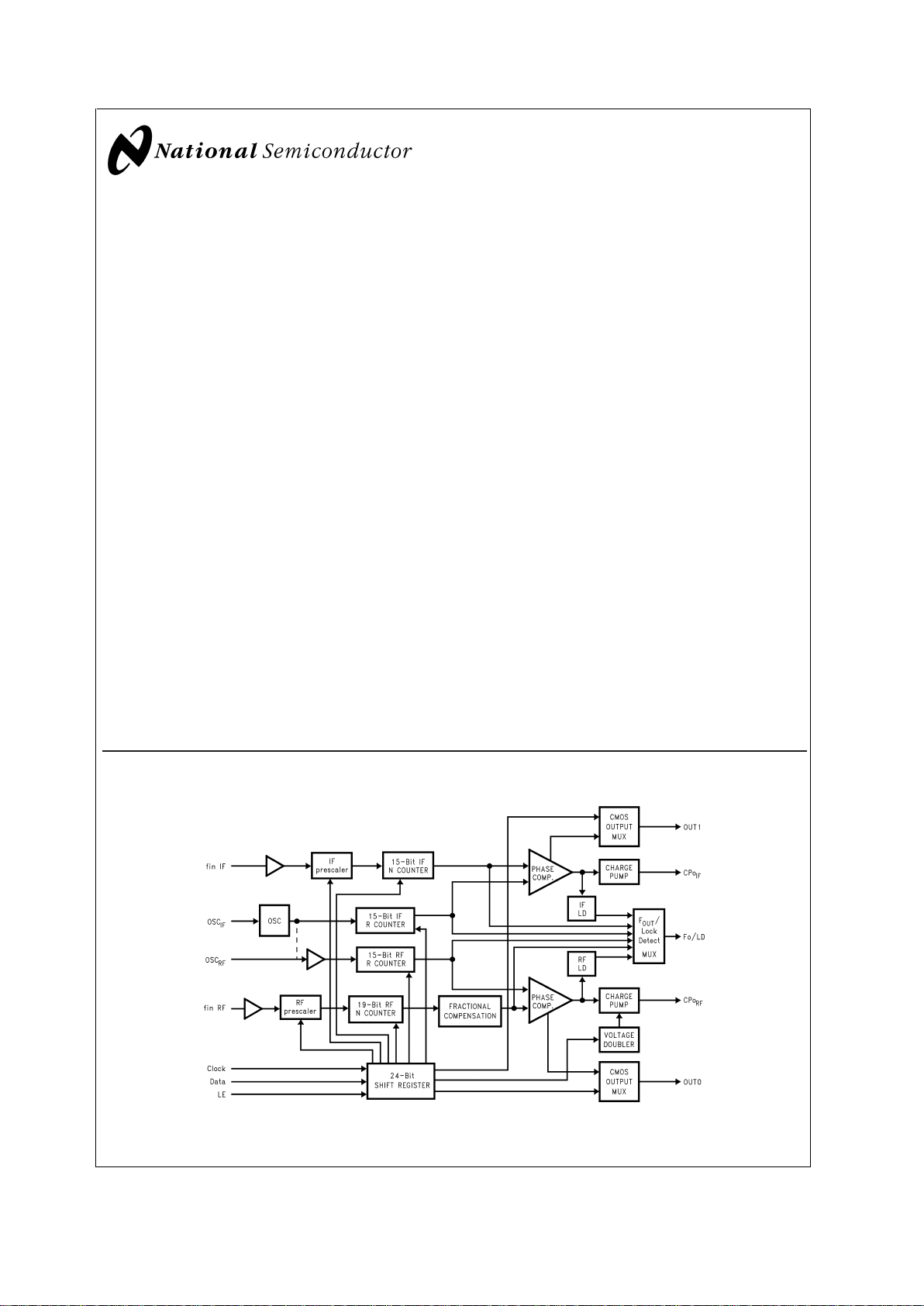
Functional Block Diagram
20004801
August 2001
LMX2354 PLLatinum Fractional N RF/ Integer N IF Dual Low Power Frequency Synthesizer
© 2001 National Semiconductor Corporation DS200048 www.national.com
Page 2
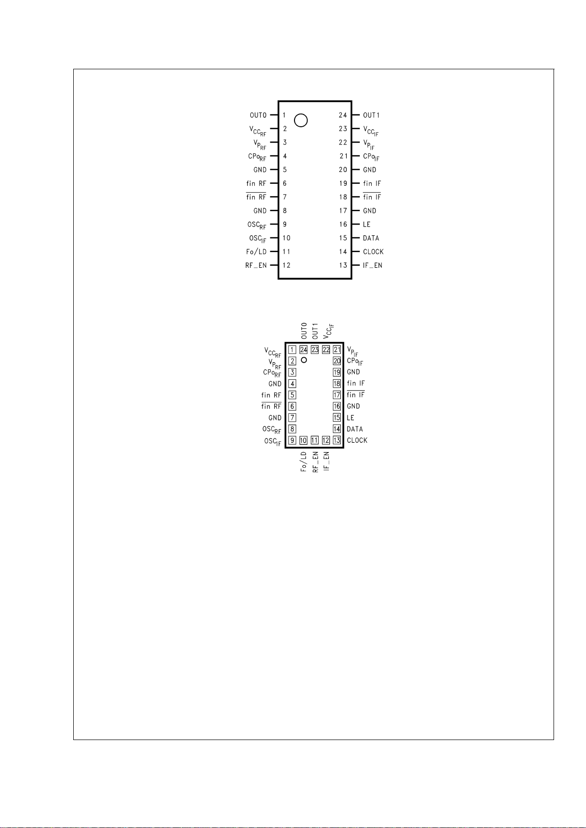
Connection Diagrams
20004802
Order Number LMX2354TM or LMX2355TM
See NS Package Number MTC24
20004822
Order Number LMX2354SLB or LMX2355SLB
See NS Package Number SLB
LMX2354
www.national.com 2
Page 3
Pin Descriptions
Pin No. for
TSSOP
Package
Pin No. for
CSP
Package
Pin
Name I/O Description
1 24 OUT0 O Programmable CMOS output. Level of the output is controlled by IF_N [17] bit.
21V
CC
RF
— RF PLL power supply voltage input. Must be equal to VccIF. May range from
2.7V to 5.5V. Bypass capacitors should be placed as close as possible to this
pin and be connected directly to the ground plane.
32V
P
RF
— Power supply for RF charge pump. Must be ≥ V
CC
RF
and V
CC
IF
.
43CP
o
RF
O RF charge pump output. Connected to a loop filter for driving the control input
of an external VCO.
5 4 GND — Ground for RF PLL digital circuitry.
6 5 fin RF I RF prescaler input. Small signal input from the VCO.
7 6 fin RF
I RF prescaler complimentary input. A bypass capacitor should be placed as
close as possible to this pin and be connected directly to the ground plane.
8 7 GND — Ground for RF PLL analog circuitry.
9 8 OSC
RF
I Dual mode oscillator output or RF R counter input. Has a VCC/2 input threshold
when configured as an input and can be driven from an external CMOS or TTL
logic gate.
10 9 OSC
IF
I Oscillator input which can be configured to drive both the IF and RF R counter
inputs or only the IF R counter depending on the state of the OSC
programming bit. (See functional description 1.1 and programming description
3.1.)
11 10 Fo/LD O Multiplexed output of N or R divider and RF/IF lock detect. CMOS output. (See
programming description 3.1.5.)
12 11 RF_EN I RF PLL Enable. Powers down RF N and R counters, prescaler, and
TRI-STATE
®
charge pump output when LOW. Bringing RF_EN high powers up
RF PLL depending on the state of RF_CTL_WORD. (See functional description
1.9.)
13 12 IF_EN I IF PLL Enable. Powers down IF N and R counters, prescaler, and TRI-STATE
charge pump output when LOW. Bringing IF_EN high powers up IF PLL
depending on the state of IF_CTL_WORD. (See functional description 1.9.)
14 13 CLOCK I High impedance CMOS Clock input. Data for the various counters is clocked
into the 24-bit shift register on the rising edge.
15 14 DATA I Binary serial data input. Data entered MSB first. The last two bits are the
control bits. High impedance CMOS input.
16 15 LE I Load Enable high impedance CMOS input. Data stored in the shift registers is
loaded into one of the 4 internal latches when LE goes HIGH. (See functional
description 1.7.)
17 16 GND — Ground for IF analog circuitry.
18 17 fin IF
I IF prescaler complimentary input. A bypass capacitor should be placed as
close as possible to this pin and be connected directly to the ground plane.
19 18 fin IF I IF prescaler input. Small signal input from the VCO.
20 19 GND — Ground for IF digital circuitry.
21 20 CPo
IF
O IF charge pump output. For connection to a loop filter for driving the input of an
external VCO.
22 21 V
PIF
— Power supply for IF charge pump. Must be ≥ V
CC
RF
and V
CC
IF
.
23 22 V
CC
IF
— IF power supply voltage input. Must be equal to V
CC
RF
. Input may range from
2.7V to 5.5V. Bypass capacitors should be placed as close as possible to this
pin and be connected directly to the ground plane.
24 23 OUT1 O Programmable CMOS output. Level of the output is controlled by IF_N [18] bit.
LMX2354
www.national.com3
Page 4
Absolute Maximum Ratings (Notes 1, 2)
Parameter Symbol
Value
Units
Min Typ Max
Power Supply Voltage V
CC
RF
−0.3 6.5 V
V
CC
IF
−0.3 6.5 V
Vp
RF
−0.3 6.5 V
Vp
IF
−0.3 6.5 V
Voltage on any pin with GND = 0V Vi −0.3 V
CC
+ 0.3 V
Storage Temperature Range Ts −65 +150 C˚
Lead Temperature (Solder 4 sec.) T
L
+260 C˚
Recommended Operating Conditions
Parameter Symbol
Value
Units
Min Typ Max
Power Supply Voltage V
CC
RF
2.7 5.5 V
V
CC
IF
V
CC
RF
V
CC
RF
V
V
pRF
V
CC
5.5 V
V
pIF
V
CC
5.5 V
Operating Temperature T
A
−40 +85 ˚C
Note 1: “Absolute Maximum Ratings” indicate limits beyond which damage to the device may occur. Operating Ratings indicate conditions for which the device is
intended tobe functional, but donot guarantee specific performancelimits. For guaranteed specificationsand test conditions, seethe Electrical Characteristics. The
guaranteed specifications apply only for the test conditions listed.
Note 2: This Device is ahigh performance RF integrated circuit with an ESDrating
<
2kV and is ESDsensitive. Handling and assembly of this device shouldonly
be done at ESD-free workstations.
Electrical Characteristics (V
cc
RF
=V
cc
IF
=V
P
RF
=V
P
IF
= 3.0V; −40˚C<T
A
<
+85˚C except as specified)
All min/max specifications are guaranteed by design, or test, or statistical methods.
Symbol Parameter Conditions
Value
Units
Min Typ Max
GENERAL
I
CC
Power Supply Current RF and IF 6.0 8.5 mA
IF Only 1.1 2.0 mA
I
CC-PWDN
Power Down Current RF_EN = IF_EN = LOW 20 50 µA
f
in
RF RF Operating Frequency 0.5 2.5 GHz
f
in
IF IF Operating Frequency 10 550 MHz
f
OSC
Oscillator Frequency No load on OSC
RF
2 50 MHz
fφ Phase Detector Frequency RF and IF 10 MHz
Pf
in RF
RF Input Sensitivity VCC= 3.0V −15 0 dBm
V
CC
= 5.0V −10 0 dBm
Pf
in IF
IF Input Sensitivity 2.7V ≤ VCC≤ 5.5V −10 0 dBm
V
OSC
Oscillator Sensitivity OSCIF, OSC
RF
0.5 V
CC
V
PP
CHARGE PUMP
ICPo-
source RF
RF Charge Pump Output
Current (see Programming
Description 3.2.2)
VCPo Vp/2, RF_CP_WORD =
0000
−100 µA
ICPo-
sink RF
VCPo = Vp/2, RF_CP_WORD =
0000
100 µA
ICPo-
source RF
VCPo = Vp/2, RF_CP_WORD =
1111
−1.6 mA
ICPo-
sink RF
VCPo = Vp/2, RF_CP_WORD =
1111
1.6 mA
LMX2354
www.national.com 4
Page 5
Electrical Characteristics (V
cc
RF
=V
cc
IF
=V
P
RF
=V
P
IF
= 3.0V; −40˚C<T
A
<
+85˚C except as specified)
All min/max specifications are guaranteed by design, or test, or statistical methods. (Continued)
Symbol Parameter Conditions
Value
Units
Min Typ Max
ICPo-
source IF
IF Charge Pump Output
Current (see Programming
Description 3.1.4)
VCPo = Vp/2, CP_GAIN_8 = 0 −100 µA
ICPo-
sink IF
VCPo = Vp/2, CP_GAIN_8 = 0 100 µA
ICPo-
source IF
VCPo = Vp/2, CP_GAIN_8 = 1 −800 µA
ICPo-
sink IF
VCPo = Vp/2, CP_GAIN_8 = 1 800 µA
ICPo-
Tri
Charge Pump TRI-STATE
Current
0.5 ≤ VCPo ≤ Vp −0.5
−40˚C
<
T
A
<
+85˚C
−2.5 2.5 nA
RF ICPo-
sink
vs. ICPo-
source
RF CP Sink vs. Source
Mismatch
VCPo = Vp/2 TA= 25˚C
RF ICPo=900µA − 1.6mA
3.5 10 %
ICPo vs. VCPo CP Current vs. Voltage
Variation
0.5 ≤ VCPo ≤ Vp −0.5
T
A
= 25˚C RF ICPo
510%
ICPo vs. T CP Current vs
Temperature
VCPo = Vp/2
−40˚C
<
T
A
<
+85˚C RF ICPo
8%
V
CP
Charge Pump Output
Voltage (RF only)
2.7V ≤ VCC≤ 3.3V, Doubler
Enabled
2*V
CC
−0.5
V
DIGITAL INTERFACE (DATA, CLK, LE, EN, FoLD)
V
IH
High-level Input Voltage (Note 3) 0.8 V
CC
V
V
IL
Low-level Input Voltage (Note 3) 0.2 V
CC
V
I
IL
Low-level Input Current VIL=0,VCC= 5.5V, (Note 3) −1.0 1.0 µA
I
IH
High-level Input Current VIH=VCC= 5.5V, (Note 3) −1.0 1.0 µA
I
IH
Oscillator Input Current VIH=VCC= 5.5V 100 µA
I
IL
Oscillator Input Current VIL=0,VCC= 5.5V −100 µA
V
OH
High-level Output Voltage IOH= −500 µA V
CC
−0.4
V
V
OL
High-level Output Voltage IOL= 500 µA 0.4 V
MICROWIRE TIMING
t
CS
Data to Clock Setup Time See Data Input Timing 50 ns
t
CH
Data to Clock Hold Time See Data Input Timing 10 ns
t
CWH
Clock Pulse Width High See Data Input Timing 50 ns
t
CWL
Clock Pulse Width Low See Data Input Timing 50 ns
t
ES
Clock to Load Enable Set
Up Time
See Data Input Timing
50 ns
t
EW
Load Enable Pulse Width See Data Input Timing 50 ns
Note 3: except fIN, OSCIFand OSC
RF
LMX2354
www.national.com5
Page 6
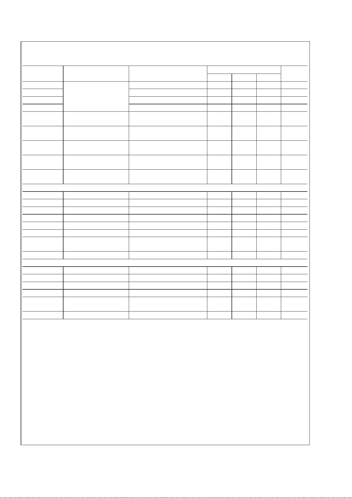
Charge Pump Current Specification Definitions
20004823
I1 = CP sink current at VDo=Vp−∆V
I2 = CP sink current at V
Do
= Vp/2
I3 = CP sink current at V
Do
= ∆V
I4 = CP source current at V
Do
=Vp−∆V
I5 = CP source current at V
Do
= Vp/2
I6 = CP source current at V
Do
= ∆V
∆V = Voltage offset from positive and negative rails. Dependent on VCO tuning range relative to V
CC
and ground. Typical values are between 0.5V and 1.0V.
Note 4: I
Do
vs VDo= Charge Pump Output Current magnitude variation vs Voltage = [1⁄
2
*
{||1| − ||3|}]/[1⁄
2
*
{||1| + ||3|}]*100% and [1⁄
2
*
{||4| − ||6|}]/[1⁄
2
*
{||4| +
||6|}]
*
100%
Note 5: I
Do-sink
vs I
Do-source
= Charge Pump Output Current Sink vs Source Mismatch = [||2| − ||5|]/[1⁄
2
*
{||2| + ||5|}]*100%
Note 6: I
Do
vs TA= Charge Pump Output Current magnitude variation vs Temperature = [||2@temp| − ||2@25˚C|]/||2@25˚C|*100% and [||5@temp| − ||5
@
25˚C|]/||5@25˚C|*100%
LMX2354
www.national.com 6
Page 7
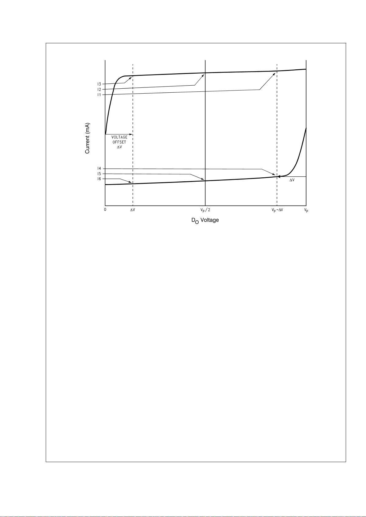
RF Sensitivity Test Block Diagram
20004824
Note: N = 10,000 R = 50 P = 16
Note: Sensitivity limit is reached when the error of the divided RF output, F
o
LD, is ≥ 1 Hz.
Typical Performance Characteristics
ICCvs V
CC
LMX2354
I
CPO
TRI-STATE vs
CP
O
Voltage
20004825 20004827
Charge Pump Current vs CPOVoltage
RF_CP_WORD = 0000 and 0111
IF CP_GAIN_8 = 0 and 1
Charge Pump Current vs CP
O
Voltage
RF_CP_WORD = 0011 and 1111
20004828
20004829
LMX2354
www.national.com7
Page 8

Typical Performance Characteristics (Continued)
Sink vs Source Mismatch
(See (Note 6) under Charge Pump Current
Specification Definitions)
RF Input Impedance
V
CC
= 2.7V to 5.5V, fIN= 550 MHz to
2.5 GHz (f
IN
Capacitor = 100 pF)
20004830
20004831
IF Input Impedance
V
CC
= 2.7V to 5.5V, fIN= 50 MHz to
550 MHz (f
IN
Capacitor = 100 pF) LMX2354 RF Sensitivity vs Frequency
20004832
20004833
LMX2354
www.national.com 8
Page 9

Typical Performance Characteristics (Continued)
IF Input Sensitivity vs Frequency Oscillator Input Sensitivity vs Frequency
20004835
20004836
LMX2354
www.national.com9
Page 10

Functional Description
1.0 GENERAL
The basic phase-lock-loop (PLL) configuration consists of a
high-stability crystal reference oscillator, a frequency synthesizer such as the National Semiconductor LMX2354, a voltage controlled oscillator (VCO), and a passive loop filter.The
frequency synthesizer includes a phase detector, current
mode charge pump, as well as programmable reference [R]
and feedback [N] frequency dividers. The VCO frequency is
established by dividing the crystal reference signal down via
the R counter to obtain a frequency that sets the comparison
frequency. This reference signal, f
r
, is then presented to the
input of a phase/frequency detector and compared with another signal, f
p
, the feedback signal, which was obtained by
dividing the VCO frequency down by way of the N counter
and fractional circuitry. The phase/frequency detector’s current source outputs pump charge into the loop filter, which
then converts the charge into the VCO’s control voltage. The
phase/frequency comparator’s function is to adjust the voltage presented to the VCO until the feedback signal’s frequency (and phase) match that of the reference signal.
When this ‘phase-locked’ condition exists, the RF VCO’s
frequency will be N+F times that of the comparison frequency, where N is the integer divide ratio and F is the
fractional component. The fractional synthesis allows the
phase detector frequency to be increased while maintaining
the same frequency step size for channel selection. The
division value N is thereby reduced giving a lower phase
noise referred to the phase detector input, and the comparison frequency is increased allowing faster switching times.
1.1 REFERENCE OSCILLATOR INPUTS
The reference oscillator frequency for the RF and IF PLLs is
provided by an external referencethroughtheOSC
IF
pin and
OSC
RF
pin. OSCIF/OSCRFblock can operate 50 MHz with
an input sensitivity of 0.5 Vpp. The OSC bit (see programming description 4.1.1), selects whether the oscillator input
pins OSC
IF
and OSCRFdrive the IF and RF R counters
separately or by a common input signal path. When an
external TCXO is connected only at the OSC
IF
input pin and
not at the OSC
RF
pin, the TCXO drives both IF R counter
and RF R counter. When configured as separate inputs, the
OSC
IF
pin drives the IF R counter while the OSCRFdrives
the RF R counter. The inputs have a V
CC
/2 input threshold
and can be driven from an externalCMOS or TTLlogicgate.
1.2 REFERENCE DIVIDERS (R COUNTERS)
The RF and IF R Counters areclockedthrough the oscillator
block either separately or in common. The maximum frequency is 50 MHz. Both R Counters are 15-bit CMOS
counters with adividerangefrom3to 32,767. (See programming description 4.1.3.)
1.3 PROGRAMMABLE DIVIDERS (N COUNTERS)
The RF and IF N Counters areclockedbythesmallsignalfin
RF and fin IF input pins respectively. The RF N Counter can
be configured as a fractional or fully integer counter. The
LMX2354 RF N counter is 19 bits with 15 bits integer divide
and 4 bits fractional.The integer part is configured as a 2-bit
A Counter, a 2-bit B Counter and a 11-bit C Counter. The
LMX2354 is capable of operating from 500 MHz to 1.2 GHz
with the 8/9/12/13 prescaler offering a continuous integer
divide range from 40 to 16,383 in fractional mode and 24 to
262143 in full integer mode. The LMX2354 is capable of
operating from 1.2 GHz to 2.5 GHz with the 16/17/20/21
prescaler offering a continuous integer divide range from 80
to 32,767 in fractional mode and 48 to 52,4287 in full integer
mode. The RF counters for the LMX2354 also contain fractional compensation, programmable in either 1/15 or 1/16
modes. The LMX2354 IF N counter is 15-bit integer divider
configured with a 3-bit A Counter and a 12-bit B Counter
offering a continuous integer divide range from 56 to 32,767
over the frequency range of 10 MHz to 550 MHz. The IF N
counter does not include fractional compensation. The
tables below show the differences between the LMX2354 in
integer mode and in quadruple modulus prescaler with P =
16/17/20/21. Also, the tables show that the bit used for the
lower modulus prescaler values is different between the
LMX2350 and the LMX2354. For the LMX2350 bit N
<9>
=0
(MSB of the A Word) is used for the 16/17 modulus and for
the LMX2354 bit N
<8>
=0 is used for the 8/9/12/13 modulus. So if the LMX2354 is replacing a LMX2350 then bits
N
<8>
and N<9>need to be swapped.
LMX2354 RF N Counter Register in Fractional Mode with P = 16/17/20/21:
C Word B Word A Word Fractional Word
N19181716151413121110987654321
1–47 Divide ratios less than 48 are impossible since it is required that C ≥3 These bits are used for
the fractional word when
the part is operated in
fractional mode
48–79 Some of these values are legal divide ratios, some are not
80* 0000000 01010000
81 0000000 01010001
...
1056 0000100 00100000
... ....... ........
32,767 1111111 11111111
*
Minimum continuous divide ratio is P•[MAX{A,B}+2]
LMX2354
www.national.com 10
Page 11

Functional Description (Continued)
LMX2354 RF N Counter Register in Fractional Mode with P = 8/9/12/13
C Word B Word A Word Fractional Word
N19181716151413121110987654321
1–23 Divide ratios less than 24 are impossible since it is required that C ≥3 These bits are used for
the fractional word when
the part is operated in
fractional mode
24–39 Some of these values are legal divide ratios, some are not
40* 0000000 01010000
41 0000000 01010001
...
272000001000100000
... ....... ........
16,383 1111111 11110111
*
Minimum continuous divide ratio is P•[MAX{A,B}+2]
1.3.1 Prescaler
The RF and IF inputs to the prescaler consist of fin and /fin;
which are complimentary inputs to differential pair amplifiers.
The complimentary inputs are internally coupled to ground
with a 10 pF capacitor.These inputs are typically AC coupled
to ground through external capacitors as well. The input
buffer drives the A counter’s ECL D-type flip flops in a dual
modulus configuration.An8/9/12/13or 16/17/20/21 prescale
ratio can be selected for the LMX2354. The IF circuitry for
both the LMX2354 contains an 8/9 prescaler. The prescaler
clocks the subsequent CMOS flip-flop chain comprising the
fully programmableA and B counters.
1.3.2 Fractional Compensation
The fractional compensation circuitry of the LMX2354 RF
dividers allows the user to adjust the VCO’stuningresolution
in 1/16 or 1/15 increments ofthe phase detector comparison
frequency. A 4-bit register is programmed with the fractions
desired numerator, while another bit selects between fractional 15 and 16 modulo base denominator (see programming description 5.2.3).An integer average is accomplished
by using a 4-bit accumulator. A variable phase delay stage
compensates for the accumulated integer phase error, minimizing the charge pump duty cycle, and reducing spurious
levels. This technique eliminates the need for compensation
current injection in to the loop filter. Overflow signals generated by the accumulator are equivalent to 1 full VCO cycle,
and result in a pulse swallow.
1.4 PHASE/FREQUENCY DETECTOR
The RF and IF phase/frequency detectors are driven from
their respective N and R counter outputs. The phase detector outputs control the charge pumps. The polarity of the
pump-up or pump-down control is programmed using
RF_PD_POL or IF_PD_POL depending on whether RF/IF
VCO characteristics are positive or negative (see programming descriptions 4.1.4 and 4.2.2). The phase detector also
receives a feedback signal from the charge pump, in order to
eliminate dead zone.
1.5 CHARGE PUMP
The phase detector’s current source outputs pump charge
into an external loop filter, which then converts the charge
into the VCO’s control voltage. The charge pumps steer the
charge pump output, CPo, to Vcc (pump-up) or ground
(pump-down). When locked, CPo is primarily in a
TRI-STATE
®
mode with small corrections. The RF charge
pump output current magnitude is programmable from
100 µA to 1.6 mA in 100 µA steps as shown in table in
programming description 4.2.2. The IF charge pump is set to
either 100 µA or 800 µA levels using bit IF_R [19] (see
programming description 4.1.4).
1.6 VOLTAGE DOUBLER
The V
pRF
pin is normally driven from an external power
supply over a rangeof V
CC
to 5.5V to providecurrent for the
RF charge pump circuit. An internal voltage doubler circuit
connected between the V
CC
and V
pRF
supply pins alter-
nately allows V
CC
=3V(±10%) users to run the RF charge
pump circuit at close to twice the V
CC
power supply voltage.
The voltage doubler mode is enabled by setting the V2_EN
bit (RF_R [22]) to a HIGH level. The voltage doubler’s
charge pump driver originates from the RF oscillator input
(OSC
RF
). The average delivery current of the doubler is less
than the instantaneous current demand of the RF charge
pump when active and is thus not capable of sustaining a
continuous out of lock condition. A large external capacitor
connected to V
pRF
(≈0.1 µF) is therefore needed to control
power supply droop when changing frequencies.
1.7 MICROWIRE
™
SERIAL INTERFACE
The programmable functions are accessed through the MICROWIRE serial interface. The interface is made of 3 functions: clock, data and latch enable (LE). Serial data for the
various counters is clocked in from data on the rising edge of
clock, into the 24-bit shift register. Data is enteredMSB first.
The last twobitsdecodetheinternalregister address. On the
rising edge of LE, data stored in the shift register is loaded
into one of the 4 appropriate latches (selected by address
bits). A complete programming description is included in the
following sections.
LMX2354
www.national.com11
Page 12

Functional Description (Continued)
1.8 Fo/LD MULTIFUNCTION OUTPUT
The Fo/LD output pin can deliver several internal functions
including analog/digital lock detects, and counter outputs.
See programming description 4.1.5 for more details.
1.8.1 Lock Detect
A digital filtered lock detect function is included with each
phase detector through an internal digital filter to produce a
logic level output available on the Fo/LD output pin if selected. Thelockdetectoutputishigh when the error between
the phase detectorinputsislessthan 15 ns for 5 consecutive
comparison cycles. The lock detect output is low when the
error between the phase detector outputs is more than 30 ns
for one comparison cycle. An analog lock detect signal is
also selectable. The lock detect output is always low when
the PLL is in power down mode. See programming descriptions 4.1.5, 5.6–5.8 for more details.
1.9 POWER CONTROL
Each PLL is individually power controlled by device enable
pins or MICROWIRE power down bits. The enable pins
override the power down bits
except for the V2_EN bit
. The
RF_EN pin controls the RF PLL; IF_EN pin controls the IF
PLL. When both pins are high, the power down bits determine the state of power control (see programming description 5.2.1.2).Activationof any PLLpowerdownmoderesults
in the disabling of the respective N counter and de-biasing of
its respective fin input (to a high impedance state). The R
counter functionality also becomes disabled whenthepower
down bit is activated. The reference oscillator block powers
down and the OSC
IF
pin reverts to a high impedance state
when both RF and IF enable pins or power down bit’s are
asserted,
unless the V2_EN bit (RF_R[22]) is high
. Power
down forces the respective charge pump and phase comparator logic to a TRI-STATE condition. A power down
counter reset function resets both N and R counters. Upon
powering up the N counter resumes counting in “close”
alignment with the R counter (The maximum error is one
prescaler cycle). The MICROWIRE control register remains
active and capable of loading and latching in data during all
of the power down modes.
2.0 Major Differences between the LMX2354 and the LMX2350/52
LMX2350/52 LMX2354
OSC
IF
Supports resonator mode. Does not support resonator mode.
Low modulus prescale (Note 7) 5-bit A counter, so if 16/17 prescale, bit-5 is
the unused place holder.
4-bit A/B counters, so if 8/9/12/13, bit-4 is
the unused place holder.
RF Prescaler LMX2350—32/33 or 16/17 LMX2354 —16/17/20/21 or 8/9/12/13
LMX2352—16/17 or 8/9
Fractional Engine Standard. Fractional Compensation cannot
be turned off.
Similar structure to the LMX2350/52, but with
some modifications for improved phase noise
and spurs. Fractional Compensation can be
turned off.
Note 7: If the LMX2354 isreplacing a LMX2350/52 in a design,and you are using the lowermodulus prescale value (16/17 on theLMX2350 changes to 8/9/12/13
on the LMX2354), the unused prescaler bit of the LMX2350/52 needs to shift down one bit from N
<9>
to N<8>.
LMX2354
www.national.com 12
Page 13

Programming Description
3.0 INPUT DATA REGISTER
The descriptions below describe the 24-bit data register loaded through the MICROWIRE Interface. The data register is used to
program the 15-bit IF_R counter register, and the 15-bit RF_R counter register, the 15-bit IF_N counter register, and the 19-bit
RF_N counter register. The data format of the 24-bit data register is shown below.The control bits CTL[1:0] decode the internal
register address. On the rising edge of LE, data stored in the shift register is loaded into one of 4 appropriate latches (selected
by address bits). Data is shifted in MSB first
MSB LSB
DATA [21:0] CTL [1:0]
23 2 1 0
3.1 Register Location Truth Table
CTL [1:0]
DATA Location
10
0 0 IF_R register
0 1 IF_N register
1 0 RF_R register
1 1 RF_N register
3.2 Register Content Truth Table
First Bit REGISTER BIT LOCATION Last Bit
23 22 21 20 19 18 17 16 15 14 13 12 11 10 9 8 7 6 5 4 3 2 1c10
c2
IF_R OSC FRAC_16 FoLD IF_CP_WORD IF_R_CNTR 0 0
IF_N IF_CTL_WORD CMOS OUTPUTS/
FRAC TEST
IF_NB_CNTR IF_NA_CNTR 0 1
RF_R DLL_MODE V2_EN RF_CP_WORD RF_R_CNTR 1 0
RF_N RF_CTL_WORD C_WORD B_WORD A_WORD FRAC_CNTR 1 1
4.0 PROGRAMMABLE REFERENCE DIVIDERS
4.1 IF_R REGISTER
If the Control Bits (CTL [1:0]) are 0 0, when data is transferred from the 24-bit shift register into a latch when LE is transitioned
high. This register determines the IF R counter value, IF Charge pump current, FoLDpinoutput,fractonalmodulus, and oscillator
mode.
MSB LSB
OSC FRAC_16 FoLD [2:0] IF_CP_WORD [1:0] IF_R_CNTR [14:0] 0 0
23 22 21 19 18 17 16 2 1 0
4.1.1 OSC (IF_R[23])
The OSC bit, IF_R [23], selects whether the oscillator inputs OSC
IF
and OSCRFdrive the IF and RF R counters separately or by
a common input signal path. When OSC=0,theOSC
IF
pin drives the IF R counter while the OSCRFpin drives the RF R counter.
When the OSC = 1, the OSC
IF
pin drives both R counters.
4.1.2 FRAC_16 (IF_R[22])
The FRAC_16 bit, IF_R [22], is used to set the fractional compensation at either 1/16 and 1/15 resolution. When FRAC-16 is set
to one, the fractional modulus is set to 1/16 resolution, and FRAC_16 = 0 corresponds to 1/15 (See section 5.2.3).
LMX2354
www.national.com13
Page 14

Programming Description (Continued)
4.1.3 15-BIT PROGRAMMABLE REFERENCE DIVIDER RATIO (R COUNTER) (IF_R[2]–IF_R[16])
IF_R_CNTR/RF_R_CNTR
Divide
Ratio
14131211109876543210
3000000000000011
4000000000000100
••••••••••••••••
32,767 111111111111111
Notes: Divide ratio: 3 to 32,767 (Divide ratios less than 3 are prohibited).
RF_R_CNTR/IF_R_CNTR These bits select the divide ratio of the programmable reference dividers.
4.1.4 IF_CP_WORD (IF_R[17]–IF_R[18])
CP_GAIN_8 IF_PD_POL
BIT LOCATION FUNCTION 0 1
CP_GAIN_8 IF_R [18] IF Charge Pump
Current Gain
1X 8X
IF_PD_POL IF_R [17] IF Phase Detector
Polarity
Negative Positive
CP_GAIN_8 is used to toggle the IF charge pump current magnitude between 1X mode (100 µA typical) and 8X mode (800 µA
typical).
IF_PD_POL is set to one when IF VCO characteristics are positive. When IF VCO frequency decreases with increasing control
voltage IF_PD_POL should set to 0.
4.1.5 FoLD* Programming Truth Table (IF_R[19]–IF_R[21])
FoLD Fo/LD OUTPUT STATE
0 0 0 IF and RF Analog Lock Detect
1 0 0 IF Digital Lock Detect
0 1 0 RF Digital Lock Detect
1 1 0 IF and RF Digital Lock Detect
0 0 1 IF R counter
1 0 1 IF N counter
0 1 1 RF R counter
1 1 1 RF N counter
*FoLD - Fout/Lock Detect PROGRAMMING BITS
4.2 RF_R Register
If the Control Bits (CTL [1:0]) are 1 0, data is transferred from the 24-bit shift register into the RF_R register latch which sets the
RF PLL’s 15-bit R counter divide ratio.The divide ratio is programmed usingthe RF_R_CNTR word as shown in table 4.1.3. The
divide ratio must be ≥ 3. The bits used to control the voltage doubler (V2_EN) and RF Charge Pump (RF_CP_WORD) are
detailed in 4.2.2.
MSB LSB
DLL_MODE V2_EN RF_CP_WORD [4:0] RF_R_CNTR [14:0] 1 0
23 22 21 17 16 2 1 0
LMX2354
www.national.com 14
Page 15

Programming Description (Continued)
4.2.1 (RF_R[22]–RF_R[23])
DLL_MODE V2_EN
BIT LOCATION FUNCTION 0 1
DLL_MODE RF_R [23] Delay Line Loop
Calibration Mode
Slow Fast
V2_EN RF_R [22] RF_Voltage Doubler
Enable
Disabled Enabled
Note 1. V2_EN bit when set high enables the voltage doubler for the RF Charge Pump supply.
Note 2. DLL_MODE bit should be set to one for normal usage.
4.2.2 RF_CP_WORD (RF_R[17]–RF_R[21])
CP_8X CP_4X CP_2X CP_1X RF_PD_POL
RF_PD_POL ( RF_R[17] )should be set to one when RF VCO characteristics are positive. When RF VCO frequency decreases
with increasing control voltage RF_PD_POL should be set to zero.
CP_1X, CP_2X, CP_4X, and CP_8X are used to step the RF Charge Pump output current magnitude from 100 µA to 1.6 mA in
100 µAsteps as shown in the table below.
RF Charge Pump Output Truth Table
ICPo µA (typ)
CP8X
RF_R[21]
CP4X
RF_R[20]
CP2X
RF_R[19]
CP1X
RF_R[18]
100 0 0 0 0
200 0 0 0 1
300 0 0 1 0
400 0 0 1 1
• ••••
900 1 0 0 0
• ••••
1600 1 1 1 1
5.0 Programmable Dividers (N Counters)
5.1 IF_N REGISTER
If the Control Bits (CTL [1:0]) are 0 1, data is transferred from the 24-bit shift register into the IF_N register latch which sets the
PLL’s15-bitprogrammable N counter value and various control functions. The IF_Ncounter consists of the 3-bit swallow counter
(A counter), and the 12-bit programmable counter (B counter). Serial data format is shown below in tables 5.1.3 and 5.1.4. The
divide ratio (IF_NB_CNTR) must be ≥ 3. The divide ratio isprogrammed using the bits IF_N_CNTR as shown in tables 5.1.2 and
5.1.3. The minimumcontinuousdivideratiois56.The CMOS [3:0] bits program the 2 CMOS outputs detailed in section 5.1.2, and
also contain the fractional test bit.
MSB LSB
IF_CTL_WORD [2:0] CMOS [3:0] IF_NB_CNTR [11:0] IF_NA_CNTR [2:0] 0 1
23 21 20 17 16 5 4 2 1 0
5.1.1 IF_CTL_WORD (IF_N[21]–IF_N[23])
MSB LSB
IF_CNT_RST PWDN_IF PWDN_MODE
Note: See section 5.2.1.2 for IF control word truth table.
LMX2354
www.national.com15
Page 16

Programming Description (Continued)
5.1.2 CMOS (Programmable CMOS outputs) (IF_N[17]–IF_N[20])
MSB LSB
FastLock TEST OUT_1 OUT_0
Note: Test bit is reserved and should be set to zero for normal usage.
5.1.3 Programmable CMOS Output Truth Table
Bit Location Function 0 1
OUT_0 IF_N[17] OUT0 CMOS Output Pin
Level Set
LOW HIGH
OUT_1 IF_N[18] OUT1 CMOS Output Pin
Level Set
LOW HIGH
Test IF_N[19] Fractional Test Bit Normal Operation No Fractional
Compensation
Fastlock IF_N[20] Fastlock Mode Select CMOS Output Fastlock Mode
Test Bit IF_N[19] controls the fractional spur compensation and should be set to 0 for normal operation. If the test bit is set to 1,
then the fractional spurs become much worse, but the phase noise improves about 5 dB.
When the Fastlock bit is set to 1, OUT_0andOUT_1 are don’t care bits. Fastlock mode utilizes the OUT0 and OUT1 outputpins
to synchronously switch between active low and TRI-STATE. The OUT0 = LOW state occurs whenever the RF loop’s CP_8X is
selected HIGH while the Fastlock bit is set HIGH (see programming description4.2.2).TheOUT0pinrevertstoTRI-STATE when
the CP_8X bit is LOW. Similarly for the IF loop, the synchronous activation of OUT1 = LOW or TRI-STATE, is dependent on
whether the CP_GAIN_8 is high or low respectively (see programming description 4.1.4).
5.1.4 3-BIT IF SWALLOW COUNTER DIVIDE RATIO (IF A COUNTER) (IF_N[2]−IF_N[4])
Swallow Count IF_NA_CNTR
(A) 2 1 0
0000
1001
••••
7111
Note: Swallow Counter Value: 0 to 7
IF_NB_CNTR ≥ IF_NA_CNTR
Minimum continuous count = 56 ( A=0, B=7)
5.1.5 12-BIT IF PROGRAMMABLE COUNTER DIVIDE RATIO (IF B COUNTER) (IF_N[5]–IF_N[16])
IF_NB_CNTR
Divide
Ratio
11109876543210
3000000000011
4000000000100
•••••••••••••
4095 111111111111
Note: Divide ratio: 3 to 4095 (Divide ratios less than 3 are prohibited)
IF_NB_CNTR ≥ IF_NA_CNTR
N divider continuous integer divide ratio 56 to 32,767.
LMX2354
www.national.com 16
Page 17

Programming Description (Continued)
5.2 RF_N Register
If the control bits (CTL[2:0]) are 1 1, data is transferred from the 24-bit shift register into the RF_N register latch which sets the
RF PLL’s programmable N counter register and various control functions. The RF N counter consists of a 2-bitAcounter, 2-bit B
counter, 11-bit C counter, and a 4-bit fractional counter. For proper operation, C_WORD^MAX{A_WORD, B_WORD}+2. Serial
data format is shown below.
MSB LSB
RF_CTL_WORD
[2:0]
C_WORD [10:0] B_WORD [1:0] A_WORD [1:0] FRAC_CONT [3:0] 1 1
23 21 20 10 9 8 7 6 5 2 1 0
5.2.1.1 RF_CTL_WORD (RF_N[21]–RF_N[23])
MSB LSB
RF_CNT_RST PWDN_RF PRESC_SEL
5.2.1.2 RF/IF Control Word Truth Table
BIT FUNCTION 0 1
IF_CNT_RST/RF_CNT_RST IF/RF counter reset Normal Operation Reset
PWDN_IF/PWDN_RF IF/RF power down Powered up Powered down
PWDN_MODE Power down mode
select
Asynchronous power
down
Synchronous power
down
PRESC_SEL LMX2354 Prescaler Modulus
Select
8/9/12/13
0.5 GHz–1.2 GHz
16/17/20/21
1.2 GHZ–2.5 GHZ
The Counter Reset enable bit when activated allows the reset of both N and R counters. Upon powering up, the N counter
resumes counting in “close” alignment with the R counter (the maximum error is one prescaler cycle).
Activation of the PLL power down bits result in the disabling of the respective N counter divider and de-biasing of its respective
fin inputs (to a high impedance state). Therespective R counter functionality also becomes disabled when the power down bit is
activated. The OSC
IF
pin reverts to a high impedance state when both RF and IF power down bits are asserted. Power down
forces the respective charge pump and phase comparator logic to a TRI-STATE condition. The MICROWIRE control register
remains active and capable of loading and latching in data during all of the power down modes.
Both synchronous and asynchronous power down modes are available with the LMX235x family in order to adapt to different
types of applications. The power down mode bit IF_N[21] is used to select between synchronous and asynchronous power down.
The MICROWIRE control register remains active and capable of loading and latching in data during all of the power down modes.
Synchronous Power Down Mode
One of the PLLloopscanbe
synchronously
powered down by first setting the power downmodebitHIGH(IF_N[21]=1)andthen
asserting its power down bit(IF_N[22] or RF_N[22] = 1). The power down function is gated by the charge pump. Once the power
down bit is loaded, the part will go into power down mode upon the completion of a charge pump pulse event.
Asynchronous Power Down Mode
One of the PLL loops can be
asynchronously
powered down by first setting the power down mode bit LOW (IF_N[21] = 0) and
then asserting its power down bit (IF_N[22] or RF_N[22] = 1).The power down function is NOTgatedby the charge pump. Once
the power down bit is loaded, the part will go into power down mode immediately.
Prescaler select is usedto set the RF prescaler. The LMX2354 contains quadruple modulus prescalers. It uses the16/17/20/21
prescaler mode to operate at 1.2 GHz–2.5 GHz. In addition, it can use the 8/9/12/13 prescaler to operate at 550 MHz–1.2 GHz.
LMX2354
www.national.com17
Page 18

Programming Description (Continued)
5.2.2 N REGISTER— (8/9/12/13) PRESCALER OPERATING IN FRACTIONAL MODE (RF_N[6]–RF_N[20])
RF_N_CNTR [14:0]
Divide
Ratio
C Word B Word A Word
1–23 Divide Ratios Less than 24 are impossible since it is required that C
>
=3
24–39 Some of these N values are Legal Divide Ratios, some are not
40000000001010000
41000000001010001
..............0...
16383 111111111110111
N REGISTER— (16/17/20/21) PRESCALER OPERATING IN FRACTIONAL MODE (RF_N[6]–RF_N[20])
RF_N_CNTR [14:0]
Divide
Ratio
C Word B Word A Word
1–47 Divide Ratios Less than 48 are impossible since it is required that C
>
=3
48–79 Some of these N values are Legal Divide Ratios, some are not
80000000001010000
81000000001010001
..............0...
32767 111111111111111
5.2.3 FRACTIONAL MODULUS ACCUMULATOR (FRAC_CNTR) (RF_N[2]–RF_N[5])
Fractional Ratio (F) FRAC_CNTR
Modulus 15 Modulus 16 RF_N[5] RF_N[4] RF_N[3] RF_N[2]
000000
1/15 1/16 0 0 0 1
2/15 2/16 0 0 1 0
••••••
14/15 14/16 1 1 1 0
N/A 15/16 1 1 1 1
LMX2354
www.national.com 18
Page 19

Programming Description (Continued)
5.3 QUADRATURE MODULUS PRESCALER
The LMX2354 contains a quadrature modulus prescaler, consisting of aprescaler, A counter, B counterand C counter. Once the
N value is known, the A, B, and C values can be calculated by:
C = N div P
B=(N–C
•
P) div 4
A = N mod 4
For the divide ratio to be legal, it is also required:
C
>
=max {A, B} + 2
fvco = [N + F] x [fosc/R]
N=P
•
C+4•B+A
F: Fractional ratio (contents of FRAC_CNTR divided by the fractional modulus)
f
vco
: Output frequency of external voltage controlled oscillator (VCO)
C: Preset value of the C counter
B: Preset value of the B counter
A: Preset value of the A counter
f
osc
: Output frequency of the external reference frequency oscillator
R: Preset divide ratio of binary 15-bit programmable reference counter (3 to 32,767)
P: Preset modulus of quadrature modulus prescaler
8/9/12/13 550 MHz–1.2 GHz
16/17/20/21 1.2 GHz–2.5 GHz
5.4 SERIAL DATA INPUT TIMING
20004803
Note: Data shifted into register on clock rising edge. Data is shifted in MSB first.
TEST CONDITIONS: The Serial Data Input Timing is tested using a symmetrical waveform around V
CC
/2. The test waveform has an edge rate of 0.6 V/ns
with amplitudes of 2.2V
@
VCC=2.7V and 2.6V@VCC= 5.5V.
LMX2354
www.national.com19
Page 20

Programming Description (Continued)
5.5 LOCK DETECT DIGITAL FILTER
The Lock Detect Digital Filter compares the difference between the phase of the inputs of the phase detector to a RC generated
delay of approximately 15 ns. To enter the locked state (Lock = HIGH) the phase error must be less than the 15 ns RC delay for
5 consecutive reference cycles. Once in lock (Lock = HIGH), the RC delay is changed to approximately 30 ns. To exit thelocked
state (Lock = LOW), the phase error must become greater than the 30 ns RC delay. When the PLL is in the power down mode,
Lock is forced LOW. A flow chart of the digital filter is shown at right.
20004804
LMX2354
www.national.com 20
Page 21

Programming Description (Continued)
5.6 ANALOG LOCK DETECT FILTER
When the Fo/LD output is configured in analog lock detect mode an external lock detect circuit is needed in order to provide a
steady LOW signal when the PLL is in the locked state. A typical circuit is shown below.
20004805
5.7 TYPICAL LOCK DETECT TIMING
20004806
LMX2354
www.national.com21
Page 22

Physical Dimensions inches (millimeters) unless otherwise noted
Thin Shrink Small Outline (TSSOP) Package
Order Number LMX2354TM
For Tape and Reel (2500 Units per Reel)
Order Number LMX2354TMX
NS Package Number MTC24
LMX2354
www.national.com 22
Page 23

Physical Dimensions inches (millimeters) unless otherwise noted (Continued)
Chip Scale Package
For Tape and Reel (2500 Units per Reel)
Order Number LMX2354SLBX
NS Package Number SLB24A
LIFE SUPPORT POLICY
NATIONAL’S PRODUCTS ARE NOT AUTHORIZED FOR USE AS CRITICAL COMPONENTS IN LIFE SUPPORT
DEVICES OR SYSTEMS WITHOUT THE EXPRESS WRITTEN APPROVAL OF THE PRESIDENT AND GENERAL
COUNSEL OF NATIONAL SEMICONDUCTOR CORPORATION. As used herein:
1. Life support devices or systems are devices or
systems which, (a) are intended for surgical implant
into the body, or (b) support or sustain life, and
whose failure to perform when properly used in
accordance with instructions for use provided in the
labeling, can be reasonably expected to result in a
significant injury to the user.
2. A critical component is any component of a life
support device or system whose failure to perform
can be reasonably expected to cause the failure of
the life support device or system, or to affect its
safety or effectiveness.
National Semiconductor
Corporation
Americas
Email: support@nsc.com
National Semiconductor
Europe
Fax: +49 (0) 180-530 85 86
Email: europe.support@nsc.com
Deutsch Tel: +49 (0) 69 9508 6208
English Tel: +44 (0) 870 24 0 2171
Français Tel: +33 (0) 1 41 91 8790
National Semiconductor
Asia Pacific Customer
Response Group
Tel: 65-2544466
Fax: 65-2504466
Email: ap.support@nsc.com
National Semiconductor
Japan Ltd.
Tel: 81-3-5639-7560
Fax: 81-3-5639-7507
www.national.com
LMX2354 PLLatinum Fractional N RF/ Integer N IF Dual Low Power Frequency Synthesizer
National does not assume any responsibility for use of any circuitry described, no circuit patent licenses are implied and National reserves the right at any time without notice to change said circuitry and specifications.
 Loading...