

Page 1
LMX2353 PLLatinum Fractional N Single 2.5 GHz Frequency Synthesizer
LMX2353
PLLatinum
™
Fractional N Single 2.5 GHz Frequency
Synthesizer
General Description
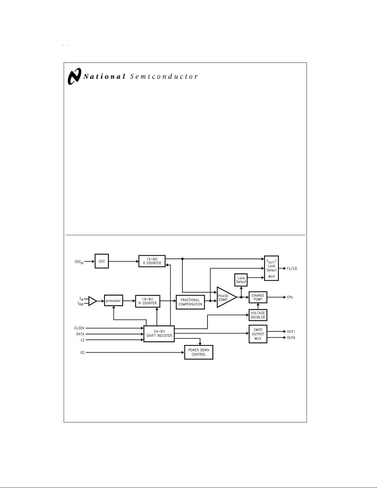
The LMX2353 is a monolithic integrated fractional N frequency synthesizer, designed to be used in a local oscillator
subsystem for a radio transceiver. It is fabricated using National’s 0.5µABiCVsiliconBiCMOS process. The LMX2353
contains dual modulus prescalers along with modulo 15 or
16 fractional compensation circuitry in the N divider. A 16/17
or 32/33 prescale ratio can be selected for the LMX2353. Using a fractional N phase locked loop technique, the LMX2353
can generate very stable low noise control signals for UHF
and VHF voltage controlled oscillators (VCO’s).
The LMX2353 has a highly flexible 16 level programmable
charge pump supplies output current magnitudes from 100
µAto 1.6 mA. Serial data is transferred into the LMX2353 via
a three wire interface (Data, LE, Clock). Supply voltage can
range from 2.7V to 5.5V. The LMX2353 features very low
current consumption; typically 4.5 mAat 3.0V. The LMX2353
is available in a 16-pin TSSOP or a 16-pad CSP surface
mount plastic package.
Functional Block Diagram
PRELIMINARY
June 1999
Features
n 2.7V – 5.5V operation
n Low Current Consumption
I
= 4.5 mA typ@VCC= 3.0V
CC
n Programmable or Logical Power Down Mode
I
=5µAtyp@VCC= 3.0V
CC
n Modulo 15 or 16 fractional N divider
Supports ratios of 1, 2, 3, 4, 5, 8, 15, or 16
n Programmable charge pump current levels
100 µA to 1.6 mA in 100 µA steps
n Digital Filtered Lock Detect
Applications
n Portable wireless communications (PCS/PCN, cordless)
n Zero blind slot TDMA systems
n Cellular and Cordless telephone systems
n Spread spectrum communication systems (CDMA)
DS101124-1
MICROWIRE™and PLLatinum™are trademarks of National Semiconductor Corporation.
®
TRI-STATE
is a registered trademark of National Semiconductor Corporation.
© 1999 National Semiconductor Corporation DS101124 www.national.com
Page 2
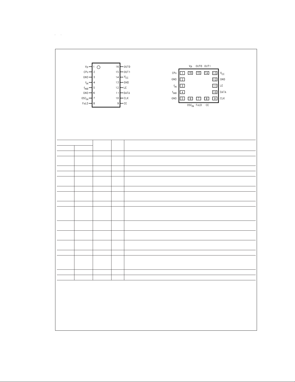
Connection Diagrams
DS101124-2
TOP VIEW
Order Number LMX2353TM or
LMX2353TMX
Order Number LMX2353SLBX
TOP VIEW
See NS Package Number SLB16A
DS101124-3
See NS Package Number MTC16
Pin Description
Pin No.
CSP TSSOP
16 1 V
12CP
2 3 GND — Ground for PLL digital circuitry.
34f
45f
5 6 GND — Ground for PLL analog circuitry.
6 7 OSC
78F
8 9 CE I PLL Enable. Powers down N and R counters, prescalers, and TRI-STATE
9 10 CLK I High impedance CMOS Clock input. Data for the various counters is clocked into
10 11 DATA I Binary serial data input. Data entered MSB first. The last two bits are the control
11 12 LE I Load enable high impedance CMOS input. Data stored in the shift registers is
12 13 GND — Ground.
13 14 V
14 15 OUT1 — Programmable CMOS output. Level of the output is controlled by F2[18] bit.
15 16 OUT0 — Programmable CMOS output. Level of the output is controlled by F2[17] bit.
Pin
Name
INB
o
I/O Description
— Power supply for charge pump. Must be ≥ VCC.
P
O Charge pump output. Connected to a loop filter for driving the control input of an
O
IN
external VCO.
I RF prescaler input. Small signal input from the VCO.
I RF prescaler complimentary input. A bypass capacitor should be placed as close
as possible to this pin and be connected directly to the ground plane.
I Oscillator input. A CMOS inverting gate input. The input has a VCC/2 input
in
threshold and can be driven from an external CMOS or TTL logic gate.
LD O Multiplexed output of N or R divider and lock detect. CMOS output.
pump output when LOW. Bringing CE high powers up PLL depending on the state
of CTL_WORD.
the 24-bit shift register on the rising edge.
bits. High impedance CMOS input.
loaded into one of the 4 internal latches when LE goes HIGH.
CC
— PLL power supply voltage input. May range from 2.7V to 5.5V. Bypass capacitors
should be placed as close as possible to this pin and be connected directly to the
ground plane.
®
charge
www.national.com 2
Page 3
Absolute Maximum Ratings (Notes 1, 2)
If Military/Aerospace specified devices are required,
please contact the National Semiconductor Sales Office/
Distributors for availability and specifications.
Power Supply Voltage
V
CC
Vp −0.3V to 6.5V
Voltage on any pin with
GND=0V (V
Storage Temperature Range (T
Lead Temperature (solder, 4 sec.) (T
) −0.3V to VCC+0.3V
I
) −65˚C to +150˚C
S
L
ESD - Human Body Model (Note 2) 2 kV
Electrical Characteristics (V
Symbol Parameter Conditions
−0.3V to 6.5V
) +260˚C
=Vp=
CC
3.0V; −40˚C
Recommended Operating
Conditions
Power Supply Voltage
V
CC
Vp V
Operating Temperature (T
Note 1: Absolute Maximum Ratings indicate limits beyond which damage to
the device may occur. Operating Ratings indicate conditions for which the device is intended to be functional, but do not guarantee specific performance
limits. For guaranteed specifications and test conditions, see the Electrical
Characteristics. The guaranteed specifications apply only for the test conditions listed.
Note 2: This device is a high performance RF integrated circuit and is ESD
sensitive. Handling and assembly of this device should only be done at ESD
free workstations.
<
<
T
85˚C except as specified).
A
) −40˚C to +85˚C
A
Value
Min Typ Max
2.7V to 5.5V
to 5.5V
CC
Unit
GENERAL
I
CC
I
CC-PWDN
f
IN
f
OSC
Power Supply Current 4.5 mA
Power Down Current CE = LOW 5 µA
RF Operating Frequency (Note 3) 0.5 2.5 GHz
Oscillator Frequency (Note 3) 2 50 MHz
fφ Phase Detector Frequency 10 MHz
Pf
IN
V
OSC
RF Input Sensitivity VCC= 3.0V −15 0 dBm
V
= 5.0V −10 0 dBm
Oscillator Sensitivity OSC
CC
IN
0.5 V
V
CC
PP
CHARGE PUMP
ICP
o-source
ICP
o-sink
ICP
o-source
ICP
o-sink
ICP
o-TRI
ICP
o-sink
ICP
o-source
vs
ICP
o
VCP
o
vs T CP Current vs Temperature VCP
ICP
o
Charge Pump Output Current VCP
Charge Pump TRI-STATE
Current
vs
CP Sink vs Source Mismatch VCP
CP Current vs Voltage 0.5 ≤ VCPo≤ Vp − 0.5, T
=
Vp/2,
o
CP_WORD = 0000
=
VCP
Vp/2,
o
CP_WORD = 0000
=
VCP
Vp/2,
o
CP_WORD = 1111
=
VCP
Vp/2,
o
CP_WORD = 1111
0.5 ≤ VCPo≤ Vp − 0.5,
<
<
T
−40˚C
o
o
A
=
Vp/2, T
=
Vp/2, −40˚C
85˚C
A
=
25˚C
=
25˚C
A
<
<
T
85˚C 8
A
−100 µA
100 µA
−1.6 mA
1.6 mA
500 pA
3
8
%
%
%
VOLTAGE DOUBLER
V
D-ON
V
CPO
V
P DOUBLER
DIGITAL INTERFACE (DATA, CLK, LE, EN, F
V
IH
V
IL
Voltage Doubler Turn on Time OSCIN= 10 MHz, C
Settled to within±10
V
P
Charge Pump Output Voltage 2.7V ≤ VCC≤ 3.3V,
Doubler Enabled
Doubler Voltage at VPPin 2.7V ≤ VCC≤ 3.3V,
Doubler Enabled
LD)
o
ext
= 0.1 µF
%
TBD µs
2xV
CC
− 1.0
2xV
CC
− 0.5
High-Level Input Voltage (Note 4) 0.8 x
V
CC
Low-Level Input Voltage (Note 4) 0.2 x
V
CC
V
V
V
V
www.national.com3
Page 4
Electrical Characteristics (V
CC
=Vp=
3.0V; −40˚C
Symbol Parameter Conditions
DIGITAL INTERFACE (DATA, CLK, LE, EN, F
I
IH
I
IL
I
IH
I
IL
V
OH
V
OL
High-Level Input Current V
Low-Level Input Current V
Oscillator Input Current VIH=VCC= 5.5V 100 µA
Oscillator Input Current VIL=0,VCC= 5.5V −100 µA
High-Level Output Voltage IOH= −500 µA VCC−
Low-Level Output Voltage IOL= 500 µA 0.4 V
LD)
o
=
=
V
IH
CC
=
0, V
IL
CC
<
<
T
85˚C except as specified). (Continued)
A
Value
Min Typ Max
5.5V, (Note 4) −1.0 1.0 µA
=
5.5V, (Note 4) −1.0 1.0 µA
0.4
MICROWIRE TIMING
t
CS
t
CH
t
CWH
t
CWL
t
ES
t
EW
Note 3: Minimum operating frequencies are not production tested — only characterized.
Note 4: Except f
Data to Clock Setup Time See Data Input Timing 50 ns
Data to Clock Hold Time See Data Input Timing 10 ns
Clock Pulse Width High See Data Input Timing 50 ns
Clock Pulse Width Low See Data Input Timing 50 ns
Clock to Load Enable Setup
Time
See Data Input Timing
50 ns
Load Enable Pulse Width See Data Input Timing 50 ns
and OSCIN.
IN
1.0 Functional Description
The basic phase-lock-loop (PLL) configuration consists of a high-stability crystal reference oscillator, a frequency synthesizer
such as the National Semiconductor LMX2353, a voltage controlled oscillator (VCO), and a passive loop filter. The frequency synthesizer includes a phase detector, current mode charge pump, as well as programmable reference [R] and feedback [N] frequency dividers. The VCO frequency is established by dividing the crystal reference signal down via the R counter to obtain a frequency that sets the comparison frequency. This reference signal, fr, is then presented to the input of a phase/frequency detector
and compared with another signal, fp, the feedback signal, which was obtained by dividing the VCO frequency down by way of
the N counter and fractional circuitry. The phase/frequency detector’s current source outputs pump charge into the loop filter,
which then converts the charge into the VCO’s control voltage. The phase/frequency comparator’s function is to adjust the voltage
presented to the VCO until the feedback signal’s frequency (and phase) match that of the reference signal. When this “phaselocked” condition exists, the RF VCO’s frequency will be N+F times that of the comparison frequency, where N is the integer divide ratio and F is the fractional component. The fractional synthesis allows the phase detector frequency to be increased while
maintaining the same frequency step size for channel selection. The division value N is thereby reduced giving a lower phase
noise referred to the phase detector input, and the comparison frequency is increased allowing faster switching times.
1.1 REFERENCE OSCILLATOR INPUT
The reference oscillator frequency for the PLL is provided by an external reference TCXO through the OSC
operate to 50 MHz with a minimum input sensitivity of 0.5 V
an external CMOS or TTL logic gate.
. The inputs have a VCC/2 input threshold and can be driven from
pp
1.2 REFERENCE DIVIDER (R-COUNTER)
The R-counter is clocked through the oscillator block. The maximum frequency is 50 MHz. The R-counter is CMOS design and
15-bit in length with programmable divider ratio from 3 to 32,767.
1.3 FEEDBACK DIVIDER (N-COUNTER)
The N counter is clocked by the small signal f
The integer part is configured as a 5-bit A counter and a 10-bit B counter. The LMX2353 is capable of operating from 500 MHz
input pin. The N counter is 19 bits with 15 bits integer divide and 4 bits fractional.
IN
to 1.2 GHz with the 16/17 prescaler offering a continuous integer divide range from 272 to 16399, and 1.2 GHz to 2.5 GHz with
the 32/33 prescaler offering a continuous integer divide range from 1056 to 32767. The fractional compensation is programmable
in either 1/15 or 1/16 modes.
1.3.1 Prescaler
The RF input to the prescaler consist of f
mentary input is internally coupled to ground with a 10 pF capacitor. This input is typically AC coupled to ground through external
IN
and f
; which are complimentary inputs to a differential pair amplifier. The compli-
INB
capacitors as well. A 16/17 or 32/33 prescaler ratio can be selected.
pin. OSCinblock can
in
Unit
V
www.national.com 4
Page 5

1.0 Functional Description (Continued)
1.3.2 Fractional Compensation
The fractional compensation circuitry in the N divider allows the user to adjust the VCO’s tuning resolution in 1/16 or 1/15 increments of the phase detector comparison frequency.A4-bit register is programmed with the fractions desired numerator, while another bit selects between fractional 15 and 16 modulo base denominator.An integer average is accomplished by using a 4-bit accumulator.Avariable phase delay stage compensates for the accumulated integer phase error, minimizing the charge pump duty
cycle, and reducing spurious levels. This technique eliminates the need for compensation current injection in to the loop filter.
Overflow signals generated by the accumulator are equivalent to 1 full VCO cycle, and result in a pulse swallow.
1.4 PHASE/FREQUENCY DETECTOR
The phase/frequency detector is driven from the N and R counter outputs. The maximum frequency at the phase detector input
is about 2 MHz for some high frequency VCO due to the minimum continuous divide ratio of the dual modulus prescaler. For example, if the VCO output frequency is 1.984 GHz, the maximum phase detector input frequency is 2 MHz because the minimum
continuous divide ratio with 32/33 prescaler is 1056. The phase detector outputs control the charge pumps. The polarity of the
pump-up or pump-down control is programmed using PD_POL depending on whether the VCO characteristics are positive or
negative. The phase detector also receives a feedback signal from the charge pump, in order to eliminate dead zone.
1.5 CHARGE PUMPS
The phase detector’s current source output pumps charge into an external loop filter, which then integrates into the VCO’s control
voltage. The charge pump steers the charge pump output CP
primarily in a TRI-STATE mode with small corrections. The charge pump output current magnitude can be selected from 100 µA
to 1.6 mA by programming the CP_WORD bits.
1.6 VOLTAGE DOUBLER
The V
pin is normally driven from an external power supply over a range of VCCto 5.5V to provide current for the RF charge
p
pump circuit. An internal voltage doubler circuit connected between the V
±
(
10%) users to run the RF charge pump circuit at close to twice the VCCpower supply voltage. The Voltage doubler mode is enabled by setting the V2_EN bit (R[20]) to a HIGH level. The average delivery current of the doubler is less than the instantaneous
current demand of the RF charge pump when active and is thus not capable of sustaining a continuous out of lock condition. A
large external capacitor connected to V
1.7 MICROWIRE
™
SERIAL INTERFACE
(≈ 0.1 µF) is therefore needed to control power supply droop when changing frequencies.
p
The programmable functions are accessed through the MICROWIRE serial interface. The interface is made of three functions:
clock, data and latch enable (LE). Serial data for the various counters is clocked in from data on the rising edge of clock, into the
24-bit shift register. Data is entered MSB first. The last two bits decode the internal register address. On the rising edge of LE,
data stored in the shift register is loaded into one of the 4 appropriate latches (selected by address bits). A complete programming
description is included in the following sections.
1.8 Lock Detect Output
A digital filtered lock detect function is included with each phase detector through an internal digital filter to produce a logic level
output available on the FoLD output pin if selected. The lock detect output is high when the error between the phase detector inputs is less than 15 ns for 5 consecutive comparison cycles. The lock detect output is low when the error between the phase detector inputs is more than 30 ns for one comparison cycle. An analog lock detect status generated from the phase detector is also
available on the FoLD output pin, if selected. The lock detect output goes high when the charge pump is inactive. It goes low when
the charge pump is active during a comparison cycle. When a PLL is in power down mode, the respective lock detect output is
always low.
1.9 OUT0/OUT1 Output Modes (Fastlock & CMOS Output Modes)
The OUT_0 and OUT_1 pins are normally used as general purpose CMOS outputs or as part of a fastlock scheme. There is also
a production test mode that overrides the other two normal modes when activated. The selection of these modes is determined
by the 4 bit CMOS register (F2_15–18) described in Table 2.5.3.
The fastlock mode allows the user to open up the loop bandwidth momentarily while acquiring lock by increasing the charge pump
output current magnitude while simultaneously switching in a second resistor element to ground via the OUT0 output pin. The
loop will lock faster without any additional stability considerations as the phase margin remains constant.
The loop bandwidth during fastlock can be opened up by as much as a factor of 4. The amount of bandwidth increase is a function
of the square root of the charge pump current increase. The maximum charge pump current ratio results from switching the
charge pump current between 100 µA and 1.6 mA. The damping resistor ratio for these two charge pump current setting changes
by the reciprocal of the bandwidth change. In the 4 to 1 bandwidth scenerio, the resulting damping resistor value would be 1/4th
of the steady state value. This would be achieved by switching 3 more identical resistors in parallel with the first to ground through
the OUT_0 pin.
to VCC(pump-up) or Ground (pump-down). When locked, CPois
o
and Vpsupply pins alternately allows VCC=3V
CC
www.national.com5
Page 6

1.0 Functional Description (Continued)
1.10 POWER CONTROL
The PLL is power controlled by the device enable pin (CE) or MICROWIRE power down bit. The enable pin overrides the power
down bit
except for the V2_EN bit.
PLL power down mode results in the disabling of the N counter and de-biasing of f
counter functionality also becomes disabled when the power down bit is activated. The reference oscillator block powers down
and the OSCin pin reverts to a high impedance state when CE or power down bit’s are asserted,
is high
. Power down forces the charge pump and phase comparator logic to a TRI-STATEcondition. A power down counter reset
function resets both N and R counters. Upon powering up the N counter resumes counting in “close” alignment with the R counter
(The maximum error is one prescaler cycle). The MICROWIRE control register remains active and capable of loading and latching
in data during all of the power down modes.
When CE is high, the power down bit determines the state of power control. Activation of any
input (to a high impedance state). The R
IN
unless the V2_EN bit (R[20])
2.0 Programming Description
2.1 MICROWIRE INTERFACE
The LMX2353 register set can be accessed through the MICROWIRE interface. A 24-bit shift register is used as a temporary register to indirectly program the on-chip registers. The shift register consists of a 24-bit DATA[21:0] field and a 2-bit ADDRESS[1:0]
field as shown below. The address field is used to decode the internal register address. Data is clocked into the shift register in
the direction from MSB to LSB, when the CLOCK signal goes high. On the rising edge of Latch Enable (LE) signal, data stored
in the shift register is loaded into the addressed latch.
MSB LSB
DATA[21:0] ADDRESS[1:0]
23 2 1 0
2.1.1 Registers’ Address Map
When Latch Enable (LE) is transitioned high, data is transferred from the 24-bit shift register into the appropriate latch depending
on the state of the ADDRESS[1:0] bits. A multiplexing circuit decodes these address bits and writes the data field to the corresponding internal register.
ADDRESS[1:0]
FIELD
0 0 F1 Register
0 1 F2 Register
1 0 R Register
1 1 N Register
REGISTER
ADDRESSED
www.national.com 6
Page 7

2.0 Programming Description (Continued)
00
Data Field Address Field
01
10
11
2.1.2 Registers’ Truth Table
Most Significant Bit SHIFT REGISTER BIT LOCATION Least Significant Bit
2322 21 201918171615141312111098765432 1 0
FoLD[2:0] These bits should be set to zero
_16
FRAC
0
F1
CMOS[3:0] These bits should be set to zero
MODE
PWDN_
00
F1_21 F1_20 F1_19 F1_18 F1_17 F1_16 F1_15 F1_14 F1_13 F1_12 F1_11 F1_10 F1_9 F1_8 F1_7 F1_6 F1_5 F1_4 F1_3 F1_2 F1_1 F1_0
F2
CP_WORD[4:0] R_CNTR[14:0]
EN
V2_
DLL_
F2_21 F2_20 F2_19 F2_18 F2_17 F2_16 F2_15 F2_14 F2_13 F2_12 F2_11 F2_10 F2_9 F2_8 F2_7 F2_6 F2_5 F2_4 F2_3 F2_2 F2_1 F2_0
MODE
R
CTL_WORD[2:0] NB_CNTR[9:0] NA_CNTR[4:0] FRAC_CNTR[3:0]
N_21 N_20 N_19 N_18 N_17 N_16 N_15 N_14 N_13 N_12 N_11 N_10 N_9 N_8 N_7 N_6 N_5 N_4 N_3 N_2 N_1 N_0
R_21 R_20 R_19 R_18 R_17 R_16 R_15 R_14 R_13 R_12 R_11 R_10 R_9 R_8 R_7 R_6 R_5 R_4 R_3 R_2 R_1 R_0
N
Note: 0 denotes setting the bit to zero.
www.national.com7
Page 8

2.0 Programming Description (Continued)
2.2 R REGISTER
If the ADDRESS[1:0] field is set to 1 0 data is transferred from the 24-bit shift register into the R register which sets the PLL’ s
15-bit R-counter divide ratio when Latch Enable (LE) signal goes high. The divide ratio is put into the R_CNTR[14:0] field and is
described in section 2.2.1. The divider ratio must be ≥ 3. The bits used to control the voltage doubler (V2_EN), Delay Lock Loop,
(DLL_MODE), Charge Pump (CP_WORD) are detailed in section 2.2.2 -2.2.4 below.
Most Significant Bit SHIFT REGISTER BIT LOCATION Least Significant Bit
23 2221201918171615141312111098765432 1 0
Data Field Address Field
DLL_
V2_
MODE
EN
R
_21R_20R_19R_18R_17R_16R_15R_14R_13R_12R_11R_10R_9R_8R_7R_6R_5R_4R_3R_2R_1R_0
2.2.1 Reference Divide Ratio (R_CNTR)
If the ADDRESS[1:0] field is set to 1 0 data is transferred MSB first from the 24-bit shift register into a latch which sets the 15-bit
R Counter, R_CNTR[14:0]. Serial data format is shown below.
Divide Ratio R_14 R_13 R_12 R_11 R_10 R_9 R_8 R_7 R_6 R_5 R_4 R_3 R_2 R_1 R_0
3 000000000000011
4 000000000000100
• •••••••••••••••
32,767 111111111111111
Note: R-counter divide ratio must be from 3 to 32,767.
2.2.2 V2_EN (R_20)
The V2_EN bit when set high enables the voltage doubler for the charge pump supply.
V2_EN R_20 Voltage Doubler Enable Disable Enabled
2.2.3 DLL_MODE (R_21)
The DLL_MODE bit should be set to 1 for normal usage.
DLL_MODE R_21
2.2.4 CP_WORD (R_15-R_19)
2.2.4.1 Charge Pump Output Truth Table
ICPOµA (typ)
CP_WORD[4:0] R_CNTR[14:0]
10
R_CNTR[14:0]
Bit Location Function 0 1
Bit Location Function 0 1
Delay Line Loop
Calibration Mode
R_19 R_18 R_17 R_16 R_15
CP_8X CP_4X CP_2X CP_1X PD_POL
R_19 R_18 R_17 R_16
CP_8X CP_4X CP_2X CP_1X
100 0000
200 0001
300 0010
400 0011
- ----
900 1000
- ----
1600 1111
Slow Fast
www.national.com 8
Page 9

2.0 Programming Description (Continued)
2.2.4.2 Phase Detector Polarity (PD_POL)
Depending upon VCO characteristics, the PD_POL (R_15) bit should be set accordingly:
When VCO characteristics are positive like (1), PD_POL should be set HIGH;
When VCO characteristics are negative like (2), PD_POL should be set LOW.
VCO CHARACTERISTICS
DS101124-4
2.3 N REGISTER
If the ADDRESS[1:0] field is set to 1 1, data is transferred from the 24-bit shift register into the N register which sets the PLL’ s
19-bit N-counter, prescaler value, counter reset, and power-down bit. The 19-bit N counter consists of a 4-bit fractional numerator,
FRAC_CNTR[3:0], a 5-bit swallow counter, A_CNTR[4:0], and a 10-bit programmable counter, B_CNTR[9:0]. Serial data format
is show below. The divide ratio (NB_CNTR) must be ≥ 3, and must be ≥ swallow counter +2; NB_CNTR ≥ (NA_CNTR +2).
Most Significant Bit SHIFT REGISTER BIT LOCATION Least Significant Bit
23 22 21 20191817161514131211109876 5 4 3 2 1 0
Data Field Address Field
CTL_WORD[2:0] NB_CNTR[9:0] NA_CNTR[4:0] FRAC_CNTR[3:0]
N
_21N_20N_19N_18N_17N_16N_15N_14N_13N_12N_11N_10N_9N_8N_7N_6N_5N_4N_3N_2N_1N_0
11
2.3.1 CTL_WORD (N_19 -N_21)
N_21 N_20 N_19
CNT_RST PWDN PRESC_SEL
2.3.2 Control Word Truth Table
Bit Location Function 0 1
PRESC_SEL N_19 Prescaler Modulus Select
16/17
(0.5 GHz to 1.2 GHz)
32/33
(1.2 GHz to 2.5 GHz)
PWDN N_20 Power Down Powered Up Powered Down
CNT_RST N_21 Counter Reset
PWDN_MODE F2_19 Power Down Mode Select
Normal
Operation
Asynchronous
Power Down
Reset
Synchronous
Power Down
2.3.2.1 Counter Reset (CNT_RST)
The Counter Reset enable bit when activated allows the reset of both N and R counters. Upon removal of the reset bit, the N
counter resumes counting in “close” alignment with the R counter (the maximum error is one prescaler cycle).
2.3.2.2 Power Down (PWDN)
Activation of the PLL PWDN bit results in the disabling of the N counter divider and de-biasing of the f
state). The R counter functionality also becomes disabled when the power down bit is activated. The OSCin pin reverts to a high
input (to a high impedance
IN
impedance state as well during power down. Power down forces the charge pump and phase comparator logic to a TRI-STATE
condition. The MICROWIRE control register remains active and capable of loading and latching in data during all of the power
down modes.
2.3.2.3 Prescaler Modulus Select (PRESC_SEL)
The PRESC_SEL bit is used to set the RF prescaler modulus value. The LMX2353 is capable of operating from 500 MHz to
1.2 GHz with the 16/17 prescaler, and 1.2 GHz to 2.5 GHz with the 32/33 prescaler selection.
www.national.com9
Page 10

2.0 Programming Description (Continued)
2.3.2.4 Power Down Mode (PWDN_MODE)
Synchronous Power Down Mode
The PLL loop can be synchronously powered down by setting the PWDN mode bit HIGH (F2_19=1) and then asserting the power
down mode bit (N20 = 1). The power down function is gated by the charge pump. Once the power down program bit is loaded,
the part will go into power down mode upon the completion of a charge pump pulse event.
Asynchronous Power Down Mode
The PLL loop can be asynchronously powered down by setting the PWDN mode bit LOW (F2_19=0) and then asserting the
power down mode bit (N20 = 1). The power down function is NOT gated by the charge pump. Once the power down program bit
is loaded, the part will go into power down mode immediately.
2.3.3 Feedback Divide Ratio (NB Counter)
NB_CNTR[9:0]
Divide Ratio N_18 N_17 N_16 N_15 N_14 N_13 N_12 N_11 N_10 N_9
3 0000000011
4 0000000100
• ••••••••••
1023 1111111111
Note: B-counter divide ratio must be ≥ 3.
NB_CNTR ≥ (NA_CNTR +2).
2.3.4 Swallow Counter Divide Ratio (NA Counter)
NB_CNTR[4:0]
Divide Ratio N_8 N_7 N_6 N_5 N_4
0 00000
1 00001
• •••••
31 11111
Note: Swallow Counter Value: 0 to 31.
NB_CNTR ≥ (NA_CNTR +2).
2.3.5 Fractional Modulus Accumulator (FRAC_CNTR)
Divide
Ratio
Divide
Ratio
FRAC_CNTR[3:0]
Modulus 15 Modulus 16 N_3 N_2 N_1 N_0
0 0 0000
1/15 1/16 0001
2/15 2/16 0010
• • ••••
14/15 14/16 1110
N/A 15/16 1111
2.3.6 Pulse Swallow Function
=
f
[N+F] x [f
VCO
: Output frequency of external voltage controlled oscillator (VCO)
f
VCO
/R] where N=(PxB) + A
OSC
F: Fractional ratio (contents of FRAC_CNTR divided by the fractional modulus)
B: Preset divide ratio of binary 10-bit programmable counter (3 to 1023)
A: Preset divide ratio of binary 5-bit swallow counter
<A<
31 {P=32};
0
<A<
15 {P=16};
0
<
B
A+2
: Output frequency of the external reference frequency oscillator
f
OSC
www.national.com 10
Page 11

2.0 Programming Description (Continued)
R: Preset divide ratio of binary 15-bit programmable reference counter (3 to 32767)
P: Preset modulus of dual modulus prescaler (P=16 or 32)
2.4 F1 REGISTER
If the ADDRESS[1:0] field is set to 0 0, data is transferred from the 24-bit shift register into the F1 register when Latch Enable (LE)
signal goes high . The F1 register sets the fractional divider denominator FRAC_16 bit and F
The rest of the bits F1_0 - F1_16, and F1_21 are Don’t Care.
Most Significant Bit SHIFT REGISTER BIT LOCATION Least Significant Bit
23 22 21201918171615141312111098765432 1 0
Data Field Address Field
FRAC
0
_16
LD
F
o
These bits should be set to zero
F1
_21F1_20F1_19F1_18F1_17F1_16F1_15F1_14F1_13F1_12F1_11F1_10F1_9F1_8F1_7F1_6F1_5F1_4F1_3F1_2F1_1F1_0
Note:0 denotes setting the bit to zero.
2.4.1 FRAC_16
The FRAC_16 bit is used to set the fractional compensation at either 1/16 or 1/15 resolution. When FRAC_16 bit is set to one,
the fractional modulus is set to 1/16 resolution, and FRAC_16 = 0 corresponds to 1/15. See section 2.3.5 for fractional divider
values.
Bit Location Function 0 1
FRAC_16 F1_20 Fractional Modulus 1/15 1/16
LD
2.4.2 F
o
LD word is used to set the function of the Lock Detect output pin according to the Table2.4.2.1 below.Open drain lock de-
The F
o
tect output is provided to indicate when the VCO frequency is in “lock”. When the loop is locked and a lock detect mode is selected, the pin is HIGH, with narrow pulses LOW. See typical Lock detect timing in section 2.4.2.4.
/ Lock Dectect output FoLD word.
out
00
2.4.2.1 F
LD Programming Truth Table
O
F1_19 F1_18 F1_17 FoLD Output State
0 0 0 Analog Lock Detect
(Open Drain)
0 0 1 Reserved
0 1 0 Digital Lock Detect
0 1 1 Reserved
1 0 0 Reserved
1 0 1 Reserved
1 1 0 N Divider Output
1 1 1 R Divider Output
Reserved - Denotes a disallowed programming condition.
2.4.2.2 Lock Detect (LD) Digital Filter
The LD Digital Filter compares the difference between the phase of the inputs of the phase detector to a RC generated delay of
approximately 15 ns. To enter the locked state (Lock = HIGH) the phase error must be less than the 15 ns RC delay for 5 consecutive reference cycles. Once in lock (Lock = HIGH), the RC delay is changed to approximately 30 ns. Toexit the locked state
(Lock = LOW), the phase error must become greater than the 30 ns RC delay. If the PLL is unlocked, the lock detect output will
be forced LOW. A flow chart of the digital filter is shown next.
www.national.com11
Page 12

2.0 Programming Description (Continued)
DS101124-5
2.4.2.3 Analog Lock Detect Filter
When the Fo/LD output is configured as analog lock detect output, an external lock detect circuit is needed in order to provide a
steady LOW signal when the PLL is in the locked state. A typical circuit is shown below. It is noticed that F
open drain output.
DS101124-6
www.national.com 12
/LD is an “active low”
o
Page 13

2.0 Programming Description (Continued)
2.4.2.4 Typical Lock Detecting Timing
DS101124-7
2.5 F2 REGISTER
If the ADDRESS[1:0] field is set to 0 1, data is transferred from the 24-bit shift register into the F2 register when Latch Enable (LE)
signal goes high. The F2 register sets the CMOS output word bit CMOS[3:0] and the power down mode bit PWDN_MODE. The
rest of the bits F2_0 - F2_14, and F2_20-F_21 are Don’t Care.
Most Significant Bit SHIFT REGISTER BIT LOCATION Least Significant Bit
2322 21 201918171615141312111098765432 1 0
Data Field Address Field
00
F2
_21F2_20F2_19F2_18F2_17F2_16F2_15F2_14F2_13F2_12F2_11F2_10F2_9F2_8F2_7F2_6F2_5F2_4F2_3F2_2F2_1F2_0
PWDN_
MODE
Note:0 denotes setting the bit to zero
CMOS[3:0] These bits should be set to zero
00
2.5.1 PWDN_MODE (F2_19)
See section 2.3.2 describing the control word and power down.
2.5.2 Programmable CMOS Outputs (F2_15–F2_18)
F2_18 F2_17 F2_16 F2_15
FastLock TEST OUT_1 OUT_0
2.5.3 OUT0/OUT1 Truth Table
Bit Location Function 0 1
OUT_0 F2_15
OUT_1 F2_16
Set the output logic level of
OUT0 pin
Set the output logic level of
OUT1 pin
LOW HIGH
LOW HIGH
TEST F2_17 Test Normal Operation Test Mode
FastLock F2_18 FastLock Mode CMOS Output Mode FastLock Mode
The CMOS[3:0] 4-bit register selects one of three modes for the OUT_0 and OUT_1 pins. The OUT_0 and OUT_1 pins are normally used as general purpose CMOS outputs or as part of a fastlock scheme. There is also a production test mode that overrides
the other two normal modes when activated.
GENERAL PURPOSE CMOS OUTPUT MODE: The general purpose CMOS output mode is selected when the Fastlock bit
(F2_F18) and TEST bit (F2_17) are set LOW. The logic levels of the OUT_0 bit (F2_15) and OUT_1 bit (F2_16) then determine
the logic states of the OUT_0 and OUT_1 pins.
FASTLOCKMODE: The Fastlock bit (F2_18) selects between the general purpose CMOS output or fastlock modes. The fastlock
mode is selected when the fastlock bit is HIGH. The fastlock mode allows the user to open up the loop bandwidth momentarily
while acquiring lock by increasing the charge pump output current magnitude while simultaneously switching in a second resistor
element to ground via the OUT0 output pin.
www.national.com13
Page 14

2.0 Programming Description (Continued)
The low gain or steadystate mode for fastlocking is defined to be whenever the charge pump current selected is less than 900
µA. The high gain or acquisition mode is defined to be whenever the charge pump current is greater or equal to 900 µA. (The logic
setting of the CP_8X bit determines which of the two gain modes the user is in.) During the acquisition phase when the CP_8X
bit is set to a HIGH state, the OUT0 output becomes active LOW thereby altering the loop’s damping resistance.
The acquisition phase is terminated by setting the CP_8X bit LOW resulting in the OUT0 output being OFF or TRI-STATE. When
in fastlock mode, the OUT_0 and OUT_1 bits are don’t care bits, and the OUT1 output is at TRI-STATE.
TEST MODE: The OUT0/OUT1 test mode occurs when the TEST bit (F2_17) is set HIGH. This mode is intended for NSC production test only. Selecting this mode overrides the FASTLOCK and GEN PURPOSE modes.
2.5.4 Serial Data Input Timing
Notes: Data shifted into register on clock rising edge.
Data is shifted in MSB first.
Test Conditions: The Serial Data Input Timing is tested using a symmetrical waveform around V
amplitudes of 2.2V@VCC= 2.7V and 2.6V VCC= 5.5V.
DS101124-8
/2. The test waveform has an edge rate of 0.6 V/ns with
cc
www.national.com 14
Page 15

Physical Dimensions inches (millimeters) unless otherwise noted
For Tube Quantity (94 Units Per Tube)
TSSOP Package
For Tape and Reel (2500 Units Per Reel)
Order Number LMX2353TM or LMX2353TMX
NS Package Number MTC16
www.national.com15
Page 16

Physical Dimensions inches (millimeters) unless otherwise noted (Continued)
For Tape and Reel (2500 Units Per Reel)
Chip Scale Package
Order Number: LMX2353SLBX
NS Package Number SLB16A
LIFE SUPPORT POLICY
LMX2353 PLLatinum Fractional N Single 2.5 GHz Frequency Synthesizer
NATIONAL’S PRODUCTS ARE NOT AUTHORIZED FOR USE AS CRITICAL COMPONENTS IN LIFE SUPPORT
DEVICES OR SYSTEMS WITHOUT THE EXPRESS WRITTEN APPROVAL OF THE PRESIDENT AND GENERAL
COUNSEL OF NATIONAL SEMICONDUCTOR CORPORATION. As used herein:
1. Life support devices or systems are devices or
systems which, (a) are intended for surgical implant
into the body, or (b) support or sustain life, and
whose failure to perform when properly used in
accordance with instructions for use provided in the
2. A critical component is any component of a life
support device or system whose failure to perform
can be reasonably expected to cause the failure of
the life support device or system, or to affect its
safety or effectiveness.
labeling, can be reasonably expected to result in a
significant injury to the user.
National Semiconductor
Corporation
Americas
Tel: 1-800-272-9959
Fax: 1-800-737-7018
Email: support@nsc.com
www.national.com
National Semiconductor
Europe
Fax: +49 (0) 1 80-530 85 86
Email: europe.support@nsc.com
Deutsch Tel: +49 (0) 1 80-530 85 85
English Tel: +49 (0) 1 80-532 78 32
Français Tel: +49 (0) 1 80-532 93 58
Italiano Tel: +49 (0) 1 80-534 16 80
National Semiconductor
Asia Pacific Customer
Response Group
Tel: 65-2544466
Fax: 65-2504466
Email: sea.support@nsc.com
National Semiconductor
Japan Ltd.
Tel: 81-3-5639-7560
Fax: 81-3-5639-7507
National does not assume any responsibility for use of any circuitry described, no circuit patent licenses are implied and National reserves the right at any time without notice to change said circuitry and specifications.
 Loading...