

Page 1
LMX2346/LMX2347
PLLatinum
™
Frequency Synthesizer for RF Personal
Communications
LMX2346 2.0 GHz
LMX2347 2.5 GHz
General Description
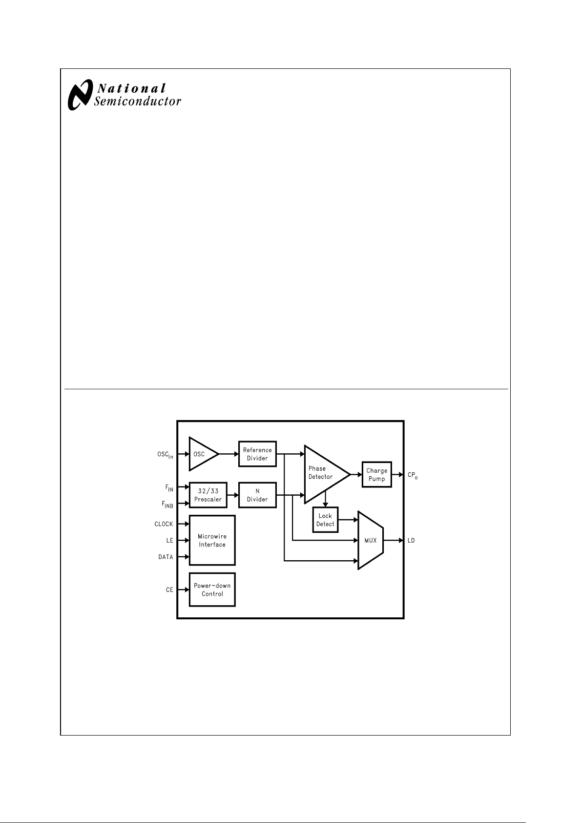
The LMX2346/7 are high performance frequency synthesizers with an integrated 32/33 dual modulus prescaler. The
LMX2346 is designed for RF operation up to 2.0 GHz. The
LMX2347 is designed for RF operation up to 2.5 GHz. Using
a proprietary digital phase locked loop technique, the
LMX2346/7 generates very stable, low noise control signals
for UHF and VHF voltage controlled oscillators.
Serial data is transferred into the LMX2346/7 via a three-line
MICROWIRE interface (DATA, LE, CLOCK). Supply voltage
range is from 2.7V to 5.5V. The charge pump provides 4 mA
output current.
The LMX2346/7 are manufactured using National’s 0.5µ
ABiC V silicon BiCMOS process and is available in 16-pin
TSSOP and 16-pin CSP packages.
Features
n RF operation up to 2.5 GHz
n 2.7V to 5.5V operation
n Digital & Analog Lock Detect
n 32/33 Dual modulus prescaler
n Excellent Phase Noise
n Internal balanced, low leakage charge pump
n Pin Compatible to LMX2323
Applications
n Cellular DCS/PCS/3G infrastructure equipment
n Wireless Local Area Networks (WLANs)
n Other wireless communication systems
Functional Block Diagram
20038406
PLLatinum™is a trademark of National Semiconductor Corporation.
November 2002
LMX2346/LMX2347 PLLatinum Frequency Synthesizer for RF Personal Communications
© 2002 National Semiconductor Corporation DS200384 www.national.com
Page 2
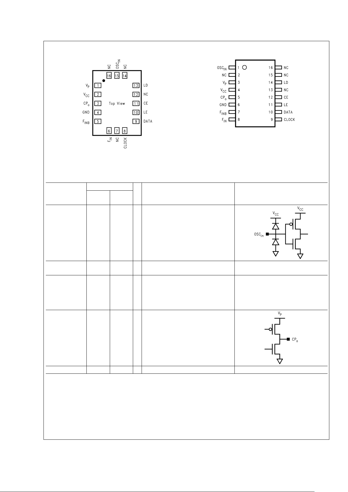
Connection Diagrams
20038407
16-Pin Chip Scale Package
NS Package Number SLB16A
20038401
16-Pin TSSOP Package
NS Package Number MTC16
Pin Descriptions
Pin Name
Pin Number
I/O Description I/O Circuit Configuration
16-Pin
CSP
16-Pin
TSSOP
OSC
IN
15 1 I Reference oscillator input. A CMOS
inverting gate input. The input has a
V
CC
/2 input threshold and can be driven
from an external CMOS or TTL logic
gate.
V
P
1 3 — Charge Pump Power Supply. Must be
equal to V
CC
.
V
CC
2 4 — Main Power Supply. VCCmay range from
2.7V to 5.5V. Bypass capacitors should
be placed as close as possible to this pin
and be connected directly to the ground
plane.
CP
o
3 5 O Charge Pump output. For connection to a
loop filter for driving the voltage control
input of an external VCO.
GND 4 6 — Ground.
LMX2346/LMX2347
www.national.com 2
Page 3
Pin Descriptions (Continued)
Pin Name
Pin Number
I/O Description I/O Circuit Configuration
16-Pin
CSP
16-Pin
TSSOP
F
INB
5 7 I RF prescaler complementary input. For
single ended operation, this pin should be
AC grounded. The LMX2346/7 can be
driven differentially when a bypass
capacitor is omitted.
F
IN
6 8 I RF PLL prescaler input. Small signal
input from the VCO.
CLOCK 8 9 I High impedance CMOS Clock input. Data
is clocked in on the rising edge, into the
18-bit shift register.
DATA 9 10 I Binary serial data input. Data entered
MSB first. LSB is control bit. High
impedance CMOS input.
LE 10 11 I Latch Enable input. When Latch Enable
transitions HIGH, data stored in the 18-bit
shift register is loaded into one of the 2
control registers, based on the address
bit. High impendance CMOS input.
CE 11 12 I Chip Enable input. Provides logical
power-down control of the device. Pull-up
to V
CC
if unused. High impedance CMOS
input.
LMX2346/LMX2347
www.national.com3
Page 4
Pin Descriptions (Continued)
Pin Name
Pin Number
I/O Description I/O Circuit Configuration
16-Pin
CSP
16-Pin
TSSOP
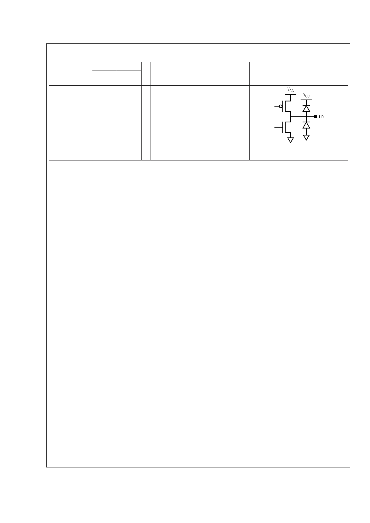
LD 13 14 O Locked Detect output. Multi-function
CMOS output pin that provides
multiplexed access to digital lock detect,
open-drain analog lock detect, as well as
the outputs of the R and N counters.
NC 7, 12, 14,162, 13, 15,16No Connect.
LMX2346/LMX2347
www.national.com 4
Page 5
Absolute Maximum Ratings (Notes 1,
2)
If Military/Aerospace specified devices are required,
please contact the National Semiconductor Sales Office/
Distributors for availability and specifications.
Power Supply Voltage,
(V
CC
) −0.3V to +6.5V
Power Supply for Charge
Pump, (V
P
) −0.3V to +6.5V
Voltage on any pin with
GND=0V, (V
i
) −0.3V to VCC+0.3V
Storage Temperature
Range, (TS) −65˚C to +150˚C
Lead Temp. (solder 4 sec.),
(T
L
) +260˚C
Recommended Operating
Conditions
(Note 1)
Min Max Unit
Power Supply Voltage, (V
CC
) 2.7 5.5 V
Power Supply for Charge Pump, (V
P
) 2.7 5.5 V
(V
P
must be equal to VCC)
Operating Temperature, (T
A
) −40 +85 ˚C
Electrical Characteristics
The following conditions apply; VCC=VP= 3.0V; −40˚C ≤ TA≤ 85˚C, unless specified differently.
Symbol Parameter Conditions Min Typ Max Units
I
CC
I
CC
Power Supply Current, LMX2346 3.5 4.5 mA
V
CC
= 5.5V 7.0 mA
Power Supply Current, LMX2347 4.5 5.5 mA
V
CC
= 5.5V 8.0 mA
I
CC
-pwdn Power Down Current CLOCK, DATA, LE = GND
CE = GND
110µA
RF PRESCALER
F
IN
Operating Frequency, RF
Prescaler, LMX2346
0.2 2.0 GHz
Operating Frequency, RF
Prescaler, LMX2347
0.2 2.5 GHz
PF
IN
Input Sensitivity, RF Prescaler 2.7V ≤ VCC≤ 3.0V (Note 6) −15 +0 dBm
3.0V
<
VCC≤ 5.5V (Note 6) −10 +0 dBm
PHASE DETECTOR
F
φ
Phase Detector Frequency 10 MHz
REFERENCE OSCILLATOR
F
OSC
Operating Frequency, Reference
Oscillator Input
(Note 10)
5 104 MHz
V
OSC
Input Sensitivity, Reference
Oscillator Input
(Note 7)
0.4 V
CC
− 0.3 V
PP
I
IH
OSCinHigh-Level Input Current VIH=VCC= 5.5V 100 µA
I
IL
OSCinLow-Level Input Current VIL= 0V, VCC= 5.5V −100 µA
CHARGE PUMP
ICPo-
source
Charge Pump Source Current VCPo = Vp/2V −4.0 mA
ICPo-
sink
Charge Pump Sink Current VCPo = Vp/2V 4.0 mA
ICPo-
tri
Charge Pump TRI-STATE Current 0.5V ≤ VCPo ≤ VP− 0.5V −2.5 2.5 nA
ICPo-
sink
vs.
ICPo-
source
CP Sink vs. Source Mismatch VCPo = Vp/2
T
A
= 25˚
(Note 4)
310%
ICPo vs
VCPo
CP Current vs. Voltage 0.5V ≤ VCPo ≤ V
P
− 0.5V
T
A
= 25˚ (Note 4)
10 15 %
ICPo vs T
A
CP Current vs. Temperature VCPo = Vp/2V (Note 4) 10 %
LMX2346/LMX2347
www.national.com5
Page 6
Electrical Characteristics (Continued)
The following conditions apply; VCC=VP= 3.0V; −40˚C ≤ TA≤ 85˚C, unless specified differently.
Symbol Parameter Conditions Min Typ Max Units
LOGICAL INTERFACE (CE, CLOCK, LE, DATA, LD)
V
IH
High-level Input Voltage 0.8 V
CC
V
V
IL
Low-level Input Voltage 0.2 V
CC
V
I
IH
High-level Input Current VIH=VCC= 5.5V −1.0 1.0 µA
I
IL
Low-level Input Current VIL= 0V, VCC= 5.5V −1.0 1.0 µA
V
OH
High-level Output Voltage IOH= −500 µA VCC− 0.4 V
V
OL
Low-level Output Voltage IOL= 500 µA 0.4 V
MICROWIRE INTERFACE (CLOCK, LE, DATA)
t
CS
Data to Clock Set Up Time (Note 5) 50 ns
t
CH
Data to Clock Hold Time (Note 5) 10 ns
t
CWH
Clock Pulse Width High (Note 5) 50 ns
t
CWL
Clock Pulse Width Low (Note 5) 50 ns
t
ES
Clock to Latch Enable Set Up
Time
(Note 5)
50 ns
t
EW
Latch Enable Pulse Width (Note 5) 50 ns
PHASE NOISE
L(f) Single Side-Band Phase Noise F
IN
= 900 MHz
F
φ
= 200 kHz
F
OSC
= 10 MHz
V
OSC
= 1.0 V
PP
TA= 25˚C (Note 3)
−91 dBc/Hz
F
IN
= 1750 MHz
F
φ
= 200 kHz
F
OSC
= 10 MHz
V
OSC
= 1.0 V
PP
TA= 25˚C (Notes 3, 9)
−86 dBc/Hz
F
IN
= 1960 MHz
F
φ
= 200 kHz
F
OSC
= 10 MHz
V
OSC
= 1.0 V
PP
TA= 25˚C (Note 3)
−85 dBc/Hz
F
IN
= 2450 MHz
F
φ
= 200 kHz
F
OSC
= 10 MHz
V
OSC
= 1.0 V
PP
TA= 25˚C (Note 3)
−83 dBc/Hz
L
N
(f) Normalized Single Side-Band
Phase Noise
Fφ= 200 kHz
F
OSC
= 10 MHz
V
OSC
= 1.0 V
PP
TA= 25˚C (Note 8)
−164.5 dBc/Hz
Note 1: Absolute Maximum Ratings indicate limits beyond which damage to the device may occur. Recommended Operating Conditions indicate conditions for
which the device is intended to be functional. For guaranteed specifications and test conditions see the Electrical Characteristics.
Note 2: This device is a high performance RF integrated circuit with an ESD rating
<
2 kV. Handling and assembly of this device should only be done at ESD
protected workstations.
Note 3: Phase Noise is measured using a reference evaluation board with a loop bandwidth of approximately 12 kHz. The phase noise specification is the
composite average of 3 measurements made at frequency offsets of 2.0, 2.5 and 3.0 kHz.
Note 4: See Charge Pump Measurement Definitions for detail on how these measurements are made.
Note 5: See Serial Input Data Timing.
Note 6: See F
IN
Sensitivity Test Setup.
Note 7: See OSC
in
Sensitivity Test Setup.
Note 8: Normalized Single-Side Band Phase Noise is defined as: L
N
(f) = L(f) − 20 log (FIN/Fφ), where L(f) is defined as the Single Side-Band Phase Noise.
Note 9: This parameter is derived from Normalized Single Side-Phase Noise, L
n
(f).
Note 10: For F
OSC
frequencies below 10 MHz, it is recommended that the rise time of the signal does not exceed 25ns.
LMX2346/LMX2347
www.national.com 6
Page 7
Typical Performance
Characteristics
ICCvs VCCLMX2346/7
20038422
CPOTRI-STATE vs CPOVoltage at 85˚C
20038423
LMX2346/LMX2347
www.national.com7
Page 8
Typical Performance Characteristics (Continued)
LMX2346/7 Charge Pump Sweeps
20038424
Sink vs Source Mismatch
(See forumla under Charge Pump Current Specifications Definitions)
20038425
LMX2346/LMX2347
www.national.com 8
Page 9
Typical Performance Characteristics (Continued)
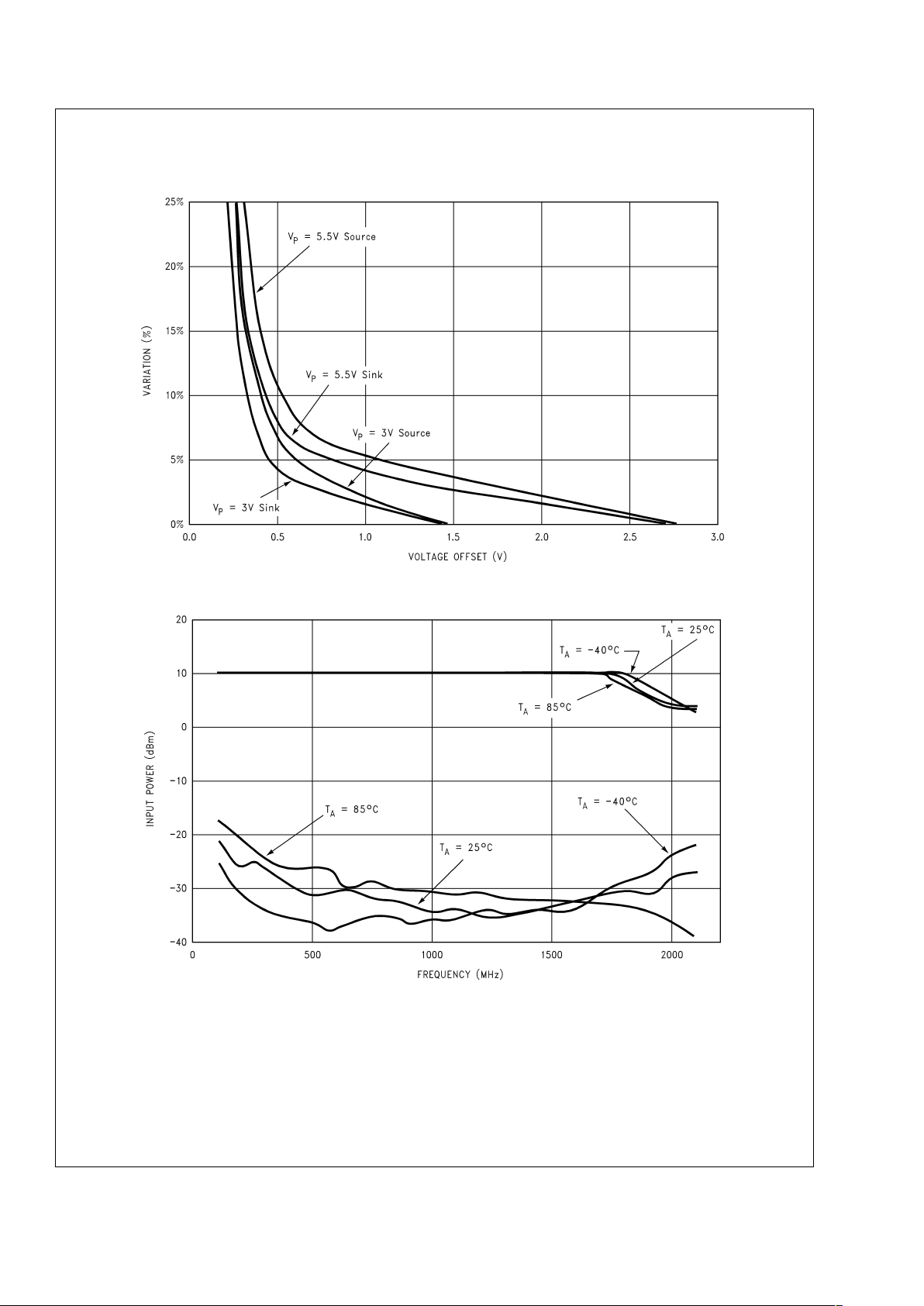
Charge Pump Current Variation
(See forumla under Charge Pump Current Specifications Definitions)
20038426
LMX2346 FINSensitivity vs Frequency at 3.0V
20038427
LMX2346/LMX2347
www.national.com9
Page 10

Typical Performance Characteristics (Continued)
LMX2346 F
IN
Sensitivity vs Frequency at 5.5V
20038428
LMX2347 FINSensitivity vs Frequency at 3.0V
20038429
LMX2346/LMX2347
www.national.com 10
Page 11

Typical Performance Characteristics (Continued)
LMX2347 F
IN
Sensitivity vs Frequency at 5.5V
20038430
LMX2346/7 OSCINSensitivity vs Frequency at 3.0V
20038431
LMX2346/LMX2347
www.national.com11
Page 12

Typical Performance Characteristics (Continued)
LMX2346/7 OSC
IN
Sensitivity vs Frequency at 5.5V
20038432
LMX2346 FINInput Impedance LMX2347 FINInput Impedance
20038433 20038434
LMX2346/LMX2347
www.national.com 12
Page 13

LMX2346/7SLB FINIMPEDANCE
LMX2346/7SLB FINIMPEDANCE
V
CC
= 3.0V (TA= 25˚C) VCC= 5.5V (TA= 25˚C)
F
IN
POWERED-UP
F
IN
POWERED-DOWN
F
IN
POWERED-UP
F
IN
POWERED-DOWN
F
IN
(MHz)
Real
ZF
IN
(Ω)
Imaginary
ZF
IN
(Ω)
|ZF
IN
|
(Ω)
Real
ZF
IN
(Ω)
Imaginary
ZF
IN
(Ω)
|ZF
IN
|
(Ω)
Real
ZF
IN
(Ω)
Imaginary
ZF
IN
(Ω)
|ZF
IN
|
(Ω)
Real
ZF
IN
(Ω)
Imaginary
ZF
IN
(Ω)
|ZF
IN
|
(Ω)
100 500 −270 568 490 −292 570 510 −270 577 492 −291 572
200 376 −256 455 365 −257 446 374 −253 452 377 −257 456
300 297 −246 386 297 −245 385 302 −245 389 300 −245 387
400 244 −234 338 245 −234 339 250 −234 342 249 −234 342
500 203 −217 297 198 −215 292 208 −218 301 207 −217 300
600 168 −198 260 168 −198 260 173 −199 264 173 −199 264
700 145 −180 231 145 −180 231 150 −182 236 148 −182 235
800 128 −163 207 129 −163 208 133 −166 213 131 −164 210
900 114 −153 191 113 −153 190 117 −154 193 116 −153 192
1000 100 −139 171 99 −140 171 103 −141 175 101 −140 173
1100 88 −125 153 88 −125 153 93 −128 158 90 −125 154
1200 80 −113 138 80 −113 138 83 −115 142 82 −114 140
1300 75 −100 125 75 −100 125 78 −102 128 76 −101 126
1400 76 −85 114 73 −84 111 79 −87 118 75 −88 116
1500 87 −83 120 85 −78 115 88 −85 122 84 −79 115
1600 80 −94 123 82 −93 124 82 −96 126 84 −92 125
1700 66 −91 112 66 −91 112 67 −92 114 69 −92 115
1800 57 −85 102 57 −84 102 59 −86 104 60 −86 105
1900 51 −79 94 51 −78 93 53 −80 96 53 −79 95
2000 46 −73 86 46 −71 85 48 −73 87 47 −73 87
2100 42 −67 79 42 −66 78 43 −68 80 43 −68 80
2200 39 −62 73 39 −62 73 41 −64 76 40 −63 75
2300 37 −58 69 37 −57 68 39 −60 72 38 −58 69
2400 35 −56 66 35 −55 65 37 −57 68 36 −56 67
2500 32 −55 64 31 −54 62 33 −57 66 32 −55 64
LMX2346/LMX2347
www.national.com13
Page 14

Typical Performance
Characteristics
LMX2346/7SLB OSCINInput Impedance vs Frequency (R_OPT= 0 or set to5-50MHz)
20038435
LMX2346/7SLB OSCINInput Impedance vs Frequency (R_OPT= 7or set to 55 - 104MHz)
20038436
LMX2346/LMX2347
www.national.com 14
Page 15

LMX2346/7SLB OSCINIMPEDANCE (R_OPT set to 5 MHz–50 MHz)
LMX2346/7SLB OSCINIMPEDANCE (R_OPT set to 5 MHz–50 MHz)
V
CC
= 3.0V (TA= 25˚C) VCC= 5.5V (TA= 25˚C)
OSC
IN
BUFFER
NORMAL OPERATION
OSCINBUFFER
POWERED-DOWN MODE
OSCINBUFFER
NORMAL OPERATION
OSCINBUFFER
POWERED-DOWN MODE
F
OSC
(MHz)
Real
ZOSC
IN
(Ω)
Imag-
inary
ZOSC
IN
(Ω)
|ZOSC
IN
|
(Ω)
Real
ZOSC
IN
(Ω)
Imag-
inary
ZOSC
IN
(Ω)
|ZOSC
IN
|
(Ω)
Real
ZOSC
IN
(Ω)
Imag-
inary
ZOSC
IN
(Ω)
|ZOSC
IN
|
(Ω)
Real
ZOSC
IN
(Ω)
Imag-
inary
ZOSC
IN
(Ω)
|ZOSC
IN
|
(Ω)
5 1100 −4800 4920 200 −6100 6100 1250 −4100 4290 100 −6200 6200
10 340 −2200 2230 80 −3000 3000 310 −1950 1970 130 −2750 2750
15 170 −1600 1610 60 −1900 1900 170 −1360 1370 50 −1970 1970
20 120 −1120 1130 35 −1400 1400 105 −1050 1060 32 −1380 1380
25 85 −953 957 28 −1150 1150 78 −840 844 28 −1130 1130
30 75 −800 804 33 −958 959 66 −704 707 28 −945 945
35 68 −692 695 30 −835 836 58 −610 613 28 −818 818
40 64 −612 615 28 −738 739 52 −538 541 28 −722 723
45 58 −530 533 27 −638 639 48 −478 480 22 −630 630
50 57 −492 495 24 −580 580 43 −422 424 21 −570 570
55 53 −447 450 23 −537 537 40 −386 388 20 −520 520
60 52 −410 413 22 −485 485 38 −354 356 18 −478 478
65 49 −373 376 22 −447 448 37 −327 329 19 −442 442
70 48 −347 350 21 −417 418 36 −303 305 18 −410 410
75 46 −326 329 20 −391 392 35 −285 287 16 −385 385
80 45 −305 308 19 −365 365 33 −266 268 16 −360 360
85 44 −289 292 18 −342 342 32 −250 252 15 −336 336
90 44 −274 278 19 −326 327 32 −236 238 16 −318 318
95 42 −260 263 18 −309 310 31 −224 226 15 −304 304
100 41 −244 247 18 −290 291 30 −212 214 15 −285 285
104 41 −234 238 17 −277 278 30 −203 205 14 −272 272
LMX2346/LMX2347
www.national.com15
Page 16

LMX2346/7SLB OSCINIMPEDANCE (R_OPT set to 50 MHz–104 MHz)
LMX2346/7SLB OSCINIMPEDANCE (R_OPT set to 50 MHz–104 MHz)
V
CC
= 3.0V (TA= 25˚C) VCC= 5.5V (TA= 25˚C)
OSC
IN
BUFFER
NORMAL OPERATION
OSCINBUFFER
POWERED-DOWN MODE
OSCINBUFFER
NORMAL OPERATION
OSCINBUFFER
POWERED-DOWN MODE
F
OSC
(MHz)
Real
ZOSC
IN
(Ω)
Imag-
inary
ZOSC
IN
(Ω)
|ZOSC
IN
|
(Ω)
Real
ZOSC
IN
(Ω)
Imag-
inary
ZOSC
IN
(Ω)
|ZOSC
IN
|
(Ω)
Real
ZOSC
IN
(Ω)
Imag-
inary
ZOSC
IN
(Ω)
|ZOSC
IN
|
(Ω)
Real
ZOSC
IN
(Ω)
Imag-
inary
ZOSC
IN
(Ω)
|ZOSC
IN
|
(Ω)
5 1500 −5750 5940 150 −6400 6400 1800 −5200 5500 225 −6200 6200
10 390 −2700 2730 110 −3000 3000 450 −2600 2640 110 −2700 2700
15 190 −2010 2020 70 −2000 2000 190 −1660 1670 75 −1850 1850
20 110 −1510 1510 30 −1400 1400 130 −1350 1360 39 −1390 1390
25 83 −1210 1210 30 −1150 1150 85 −1100 1100 26 −1120 1120
30 62 −972 974 32 −967 968 72 −926 929 27 −945 945
35 53 −842 844 31 −835 836 59 −802 804 25 −822 822
40 50 −743 745 29 −736 737 50 −705 707 26 −724 724
45 44 −658 659 26 −640 641 44 −630 632 22 −630 630
50 39 −597 598 24 −595 595 37 −558 559 22 −573 573
55 35 −541 542 23 −538 538 33 −510 511 21 −522 522
60 33 −490 491 23 −485 486 30 −468 469 20 −479 479
65 30 −459 460 22 −450 451 28 −431 432 18 −441 441
70 30 −420 421 21 −417 418 26 −402 403 17 −412 412
75 28 −394 395 20 −392 393 25 −378 379 17 −386 386
80 27 −369 370 19 −366 366 23 −352 353 16 −361 361
85 27 −349 350 19 −342 343 21 −330 331 15 −338 338
90 27 −330 331 19 −323 324 21 −311 312 15 −318 318
95 25 −312 313 18 −309 310 21 −298 299 16 −305 305
100 24 −294 295 18 −290 291 19 −280 281 14 −286 286
104 24 −280 281 18 −278 279 19 −267 268 14 −274 274
LMX2346/LMX2347
www.national.com 16
Page 17

Charge Pump Current Specification Definitions
20038437
I1 = Charge Pump Sink Current at VCPo=VP− ∆V
I2 = Charge Pump Sink Current at VCP
o=VP
/2
I3 = Charge Pump Sink Current at VCP
o
= ∆V
I4 = Charge Pump Source Current at VCP
o=VP
− ∆V
I5 = Charge Pump Source Current at VCP
o=VP
/2
I6 = Charge Pump Source Current at VCP
o
= ∆V
∆V = Voltage offset from the positive and negative rails. Dependent on the VCO tuning range relative to V
CC
and GND. Typical values are between 0.5V and
1.0V.
Charge Pump Output Current Magnitude Variation Vs Charge Pump Output Voltage
20038463
Charge Pump Output Current Sink Vs Charge Pump Output Current Source Mismatch
20038464
Charge Pump Output Current Magnitude Variation Vs Temperature
20038465
LMX2346/LMX2347
www.national.com17
Page 18

Serial Data Input Timing
20038410
Notes:
1. Data is shifted into register on clock rising edge.
2. Data is shifted in MSB first.
FINSensitivity Test Setup
20038412
Notes:
1. Test Conditions: NA_CNTR = 16, NB_CNTR = 312, LD_OUT = 3, PD = 0.
2. Sensitivity limit is reached when the frequency error of the divided RF input is greater than or equal to 1 Hz.
LMX2346/LMX2347
www.national.com 18
Page 19

OSCINSensitivity Test Setup
20038413
Notes:
1. Test Conditions: R_CNTR = 1000, LD_OUT = 2, PD = 0.
2. Sensitivity limit is reached when the frequency error of the divided RF input is greater than or equal to 1 Hz.
1.0 Functional Description
The basic phase-lock-loop (PLL) configuration consists of a
high-stability crystal reference oscillator, a frequency synthesizer such as the National Semiconductor LMX2346/7, a
voltage controlled oscillator (VCO), and a passive loop filter.
The frequency synthesizer includes a phase detector, current mode charge pump, a programmable reference divider,
and a programmable feedback divider. The VCO frequency
is established by dividing the crystal reference signal down
via the reference divider to obtain a frequency that sets the
comparison frequency. This reference signal, f
r
, is then presented to the input of a phase/frequency detector and compared with another signal, f
p
, the feedback signal, which was
obtained by dividing the VCO frequency down by way of the
feedback divider. The phase/frequency detector measures
the phase error between the f
r
and fpsignals and outputs
control signals that are directly proportional to the phase
error. The charge pump then pumps charge into or out of the
loop filter based on the magnitude and direction of the phase
error. The loop filter converts the charge into a stable control
voltage for the VCO. The phase/frequency detector’s function is to adjust the voltage presented to the VCO until the
feedback signal’s frequency and phase match that of the
reference signal. When this “phase-locked” condition exists,
the RF VCO’s frequency will be N times that of the comparison frequency, where N is the feedback divider ratio.
20038440
LMX2346/LMX2347
www.national.com19
Page 20

1.0 Functional Description (Continued)
1.1 REFERENCE OSCILLATOR
The reference oscillator frequency for the PLL is provided
from an external source via the OSC
in
pin. The reference
buffer circuit supports input frequencies from 5 MHz to 104
MHz with a minimum input sensitivity of 0.4 V
PP
. The refer-
ence buffer circuit has a V
CC
/2 input threshold and can be
driven from an external CMOS or TTL logic gate. The
R_OPT control word is used to optimize the performance of
the reference buffer circuit for best Phase Noise and power
consumption performance based on the frequency of the
reference source. Refer to Section 2.2.5 for details on programming the R_OPT control word.
1.2 REFERENCE DIVIDER (R COUNTER)
The reference divider is comprised of a 10-bit CMOS binary
counter that supports a continuous integer divide range from
2 to 1,023. The divide ratio should be chosen such that the
maximum phase comparison frequency of 10 MHz is not
exceeded. The reference divider circuit is clocked by the
output of the reference buffer circuit. The output of the
reference divider circuit feeds the reference input of the
phase detector circuit. The frequency of the reference input
to the phase detector (also referred to as the comparison
frequency) is equal to reference oscillator frequency divided
by the reference divider ratio. Refer to Section 2.2.1 for
details on programming the R Counter.
1.3 RF PRESCALER
The LMX2346/7 contain a fixed 32/33 dual modulus RF
prescaler. The RF Prescaler operates from 100 MHz to 2000
MHz on the LMX2346 and from 100 MHz to 2500 MHz on
the LMX2347.
The complementary F
IN
and F
INB
input pins drive the input of
a bipolar, differential-pair amplifier. The output of the bipolar,
differential-pair amplifier drives a chain of ECL D-type flipflops in a dual modulus configuration. The output of the
prescaler is used to clock the subsequent programmable
feedback divider.
1.4 PROGRAMMABLE FEEDBACK DIVIDER
(N COUNTER)
The programmable feedback divider operates in concert with
the RF prescaler to divide the input RF signal (F
IN
)bya
factor of N. The output of the programmable reference divider is provided to the feedback input of the phase detector
circuit. The programmable divider supports a continuous
integer divide range from 992 to 32,767. The divide ratio
should be chosen such that the maximum phase comparison
frequency (Fφ) of 10 MHz is not exceeded.
The programmable divider circuit is comprised of an A
Counter and a B Counter. The A counter is a 5-bit CMOS
swallow counter programmable from 0 to 31. The B Counter
is a 10-bit CMOS binary counter, programmable from 3 to
1023. Divide ratios less than 992 are achievable as long as
the binary counter value is greater or equal to the swallow
counter value (NB_CNTR ≥ NA_CNTR). Refer to Section
2.3.2 and 2.3.3 for details on programming the NA and NB
Counter. The following equations are useful in determining
and programming a particular value of N:
N = (32 x NB_CNTR) + NA_CNTR
F
IN
=NxF
φ
Definitions
F
φ
Phase Detector Comparison Frequency
F
IN
RF Input Frequency
NA_CNTR A Counter Value
NA_CNTR B Counter Value
1.5 PHASE/FREQUENCY DETECTOR
The phase/frequency detector is driven from the N and R
counter outputs. The maximum frequency at the phase detector inputs is 10 MHz. The phase detector outputs control
the charge pump. The polarity of the pump-up or pump-down
control signals are programmed using the PD_POL control
bit, depending on whether the RF VCO tuning characteristics
are positive or negative (see programming description in
Section 2.2.3). The phase/frequency detector has a detection range of −2π to +2π.
Phase Comparator And Internal Charge Pump Characteristics
20038411
Note 11: The minimum width of the pump up and pump down current pulses occur at the CPo pin when the loop is phase-locked.
Note 12: The diagram assumes that PD_POL = 1
Note 13: f
R
is the phase comparator input from the R Divider
Note 14: f
P
is the phase comparator input from the N Divider
Note 15: CPo is charge pump output
1.6 CHARGE PUMP
The charge pumps directs charge into or out of an external
loop filter. The loop filter converts the charge into a stable
control voltage which is applied to the tuning input of a VCO.
The charge pump steers the VCO control voltage towards V
P
during pump-up events and towards GND during pumpdown events. When locked, CPo is primarily in a Tri-state
condition with small corrections occurring at the phase comparison rate.
LMX2346/LMX2347
www.national.com 20
Page 21

1.0 Functional Description (Continued)
1.7 MICROWIRE INTERFACE
The programmable register set is accessed via the
Microwire serial interface. The interface is comprised of
three signal pins: CLOCK, DATA, and LE (Latch Enable).
Serial data is clocked in from DATA on the rising edge of
CLOCK, into an 18-bit shift register. The serial data is
clocked in MSB first. The last bit of data decodes the internal
register address. On the rising edge of LE, the data stored in
the shift register is loaded into one of the two appropriate
latches based on the address bit. A complete programming
description is provided in Section 2.0.
1.8 MULTI-FUNCTION OUTPUT
The LMX2346/7 LD pin is a multi-function output that can be
configured as a digital lock detect, an analog lock detect, as
well as monitor the output of the reference divider, or feedback divider circuits. The LD_OUT control word is used to
select the desired output function. When the PLL is in powerdown mode, the LD output is always set to a high impedance. A complete programming description of the multifunction output is provided in Section 2.2.4.
1.8.1 Analog Lock Detect
When LD_OUT = 1, an analog lock detect status generated
from the phase detector is available on the LD output pin.
The lock detect output goes to high impedance when the
charge pump is inactive. It goes low when the charge pump
is active during a comparison cycle. The analog lock detect
signal output is an open drain configuration.
1.8.2 Digital Lock Detect
When LD_OUT = 0, a digital lock detect status is available
on the LD output pin. The digital lock detect filter compares
the phase difference of the inputs from the phase detector to
a RC generated delay of approximately 15 ns. To enter the
locked state (LD = High), the phase error must be less than
the 15 ns RC delay for 5 consecutive reference cycles. Once
in lock, the RC delay is changed to approximately 30 ns. To
exit the locked state, the phase error must be greater than
the 30 ns RC delay. A flow chart of the digital lock detect filter
follows.
20038405
LMX2346/LMX2347
www.national.com21
Page 22

1.0 Functional Description (Continued)
1.9 POWER-DOWN
CE PD[1:0] Operating Mode
0 X Power-down (Asynchronous)
1 0 Normal Operation
1 1 Power-down (Synchronous)
1 2 Counter Reset
1 3 Power-down (Asynchronous)
The LMX2346/7 are power controlled through logical control
of the CE pin in conjunction with programming of the PD
control word. A truth table is provided that describes how the
state of the CE pin and the PD control word set the operating
mode of the device. A complete programming description for
the PD control word is provided in Section 2.3.1.
When the device enters the power-down mode, the oscillator
buffer, RF prescaler, phase detector, and charge pump circuits are all disabled. The OSC
IN
,CPO,FIN,F
INB
, LD pins
are all forced to a high impedance state. The reference
divider and feedback divider circuits are disabled and held at
the load point during power-down. When the device is programmed to normal operation, the oscillator buffer, RF prescaler, phase detector, and charge pump circuits are all powered on. The feedback divider and the reference divider are
held at the load point. This allows the RF Prescaler, feedback divider, reference oscillator, and the reference divider
circuitry to reach proper bias levels. After a 1.5 µs delay, the
feedback and reference divider are enabled and they resume counting in “close” alignment (The maximum error is
one prescaler cycle). The MICROWIRE control register remains active and capable of loading and latching in data
while in the power-down mode.
The synchronous power-down function is gated by the
charge pump. When the device is configured for synchronous power-down, the device will enter the power-down
mode upon the completion of the next charge pump pulse
event.
The asynchronous power-down function is NOT gated by the
completion of a charge pump pulse event. When the device
is configured for asynchronous power-down, the part will go
into power down mode immediately.
A counter reset function is provided. When the PD control
word is programmed to Counter Reset, both the feedback
divider and the reference divider are disabled and held at
their load point. When the device is programmed to normal
operation, both the feedback divider and the reference divider are enabled (without a delay) and resume counting in
“close” alignment (The maximum error is one prescaler
cycle).
2.0 Programming Description
2.1 MICROWIRE INTERFACE
The MICROWIRE interface is comprised of an 18-bit shift register, and two control registers. The shift register consists of a 17-bit
DATA field and a 1-bit address (ADDR) field as shown below. When Latch Enable transitions HIGH, data stored in the shift register
is loaded into either the R or N register depending on the state of the ADDR bit. The data is loaded MSB first. The DATA field
assignments for the R and N registers are shown in Section 2.1.1.
MSB LSB
DATA ADDR
17 1 0
ADDR Target Register
1 R register
0 N register
2.1.1 Register Map
Register Most Significant Bit SHIFT REGISTER BIT LOCATION Least Significant Bit
17 16 15 14 13 12 11 10 9 8 7 6 5 4 3 2 1 0
Data Field ADDR
R R_OPT [2:0] LD_OUT [1:0] PD_POL CP_TRI R_CNTR [9:0] 1
N NB_CNTR [9:0] NA_CNTR [4:0] PD [1:0] 0
2.2 R REGISTER
The R register contains the R_CNTR, CP_TRI, PD_POL, LD_OUT, R_OPT control words. The detailed descriptions and
programming information for each control word is discussed in the following sections.
Register Most Significant Bit SHIFT REGISTER BIT LOCATION Least Significant Bit
17161514 13 12 11 109876543210
Data Field ADDR
R R_OPT [2:0] LD_OUT [1:0] PD_POL CP_TRI R_CNTR [9:0] 1
LMX2346/LMX2347
www.national.com 22
Page 23

2.0 Programming Description (Continued)
2.2.1 R_CTR[9:0] Reference Divider (R COUNTER) R[10:1]
The reference divider can be programmed to support divide ratios from 2 to 1023. Divide ratios of less than 2 are prohibited.
R_CNTR [9:0]
Reference Divider Ratio 9876543210
2 0000000010
3 0000000011
• ••••••••••
1,023 1111111111
2.2.2 CP_TRI Charge Pump TRI-STATE R[11]
The CP_TRI control bit allows the charge pump to be switched between a normal operating mode and a high impedance output
state. This happens asynchronously or immediately with the change in CP_TRI bit.
Control Bit Register Location Description
Function
01
CP_TRI R[11] Charge Pump
TRI-STATE
Charge Pump Operates
Normal
Charge Pump Output
in High Impedance
State
2.2.3 PD_POL Phase Detector Polarity R[12]
The PD_POL control bit is used to set the polarity of the phase detector based on the VCO tuning characteristic.
Control Bit Register Location Description
Function
01
PD_POL R[12] Phase Detector
Polarity
Negative VCO Tuning
Characteristic
Positive VCO Tuning
Characteristic
VCO Characteristics
20038409
2.2.4 LD_OUT[1:0] LD Output Select R[14:13]
The LD_Out control word is used to select which signal is routed the the LD pin.
LD_OUT[1:0] LD Pin Output Mode
Output Circuit
Configuration
0 Digital Lock Detect Push-Pull
1 Analog Lock Detect Open-Drain
2 R divider output Push-Pull
3 N divider output Push-Pull
LMX2346/LMX2347
www.national.com23
Page 24

2.0 Programming Description (Continued)
2.2.5 R_OPT[2:0] Reference Oscillator Optimization R[17:15]
The R_OPT control words are used to optimize the performance of the reference buffer circuit for best Phase Noise and power
consumption performance based on the frequency of the reference source.
R_OPT[2:0]
Optimization Frequency
Range
0 5 MHz–50 MHz
7 50 MHz–104 MHz
1-6 Reserved— Do not use.
2.3 N REGISTER
The N register contains the PD (Power-Down), NA_CNTR, and NB_CNTR control words. The NA_CNTR, and NB_CNTR control
words are used to setup the programmable feedback divider. The PWR-DN control word is used to switch the device between the
normal operating mode and various power-down modes.
Register Most Significant Bit SHIFT REGISTER BIT LOCATION Least Significant Bit
17 16 15 14 13 12 11 10 9 8 7 6 5 4 3 2 1 0
Data Field ADDR
N NB_CNTR [9:0] NA_CNTR [4:0] PD [1:0] 0
2.3.1 PD[1:0] Power-Down N[2:1]
The PD control word is used to switch the device between the normal operating mode and various power-down modes.
PD [1:0] Operating Mode
0 Normal Operation
1 Synchronous Power-down
2 Counter Reset
3 Asynchronous Power-down
2.3.2 NA_CNTR[4:0] A Counter N[7:3]
The NA_CNTR control word is used to program the A counter. TheA counter is a 5-bit swallow counter used in the programmable
feedback divider. The A counter can be programmed to values ranging from 0 to 31. See Section 1.4 for details on how the value
of the A counter should be selected.
A Counter Value NA_CNTR[4:0]
0 00000
1 00001
• •••••
31 11111
2.3.3 NB_CNTR[9:0] B Counter N[17:8]
The NB_CNTR control word is used to program the B counter. The B counter is a 10-bit binary counter used in the programmable
feedback divider. The B counter can be programmed to values ranging from 3 to 1023. See Section 1.4 for details on how the
value of the B counter should be selected.
B Counter Value NB_CNTR[9:0]
3 0000000011
4 0000000100
• ••••••••••
1023 1111111111
LMX2346/LMX2347
www.national.com 24
Page 25

Order Information
Order Number Package Type Packing Information
LMX2346TM TSSOP-16
MTC16
94 Units per rail carrier
LMX2346TMX TSSOP-16
MTC16
2500 Units, Tape & Reel
LMX2346SLBX CSP-16
SLB16A
2500 Units, Tape & Reel
LMX2347TM TSSOP-16
MTC16
94 Units per rail carrier
LMX2347TMX TSSOP-16
MTC16
2500 Units, Tape & Reel
LMX2347SLBX CSP-16
SLB16A
2500 Units, Tape & Reel
LMX2346/LMX2347
www.national.com25
Page 26

Physical Dimensions inches (millimeters) unless otherwise noted
16-Pin Thin Shrink Small Outline Package
Order Number LMX2346TM, LMX2346TMX
NS Package Number MTC16
LMX2346/LMX2347
www.national.com 26
Page 27

Physical Dimensions inches (millimeters) unless otherwise noted (Continued)
16-Pin Chip Scale Package
Order Number LMX2346SLB or LMX2347SLB
For Tape and Reel (2500 Units Per Reel)
Order Number LMX2346SLBX or LMX2347SLBX
NS Package Number SLB16A
LIFE SUPPORT POLICY
NATIONAL’S PRODUCTS ARE NOT AUTHORIZED FOR USE AS CRITICAL COMPONENTS IN LIFE SUPPORT
DEVICES OR SYSTEMS WITHOUT THE EXPRESS WRITTEN APPROVAL OF THE PRESIDENT AND GENERAL
COUNSEL OF NATIONAL SEMICONDUCTOR CORPORATION. As used herein:
1. Life support devices or systems are devices or
systems which, (a) are intended for surgical implant
into the body, or (b) support or sustain life, and
whose failure to perform when properly used in
accordance with instructions for use provided in the
labeling, can be reasonably expected to result in a
significant injury to the user.
2. A critical component is any component of a life
support device or system whose failure to perform
can be reasonably expected to cause the failure of
the life support device or system, or to affect its
safety or effectiveness.
National Semiconductor
Corporation
Americas
Email: support@nsc.com
National Semiconductor
Europe
Fax: +49 (0) 180-530 85 86
Email: europe.support@nsc.com
Deutsch Tel: +49 (0) 69 9508 6208
English Tel: +44 (0) 870 24 0 2171
Français Tel: +33 (0) 1 41 91 8790
National Semiconductor
Asia Pacific Customer
Response Group
Tel: 65-2544466
Fax: 65-2504466
Email: ap.support@nsc.com
National Semiconductor
Japan Ltd.
Tel: 81-3-5639-7560
Fax: 81-3-5639-7507
www.national.com
LMX2346/LMX2347 PLLatinum Frequency Synthesizer for RF Personal Communications
National does not assume any responsibility for use of any circuitry described, no circuit patent licenses are implied and National reserves the right at any time without notice to change said circuitry and specifications.
 Loading...