

查询LMX2310供应商
LMX2310U/LMX2311U/LMX2312U/LMX2313U
December 2003
LMX2310U/LMX2311U/LMX2312U/LMX2313U PLLatinum Ultra Low Power Frequency Synthesizer
for RF Personal Communications
PLLatinum
™
Ultra Low Power Frequency Synthesizer for
RF Personal Communications
LMX2310U 2.5 GHz LMX2311U 2.0 GHz
LMX2312U 1.2 GHz LMX2313U 600 MHz
General Description
The LMX2310/1/2/3U are high performance frequency synthesizers. The LMX2310/1/2U use a selectable, dual modulus 32/33 and 16/17 prescaler. The LMX2313U uses a selectable, dual modulus 16/17 and 8/9 prescaler. The device,
when combined with a high quality reference oscillator and a
voltage controlled oscillator, generates very stable, low noise
local oscillator signals for up and down conversion in wireless communication devices.
Serial data is transferred into LMX2310/1/2/3U via a threewire interface (Data, Enable, Clock) that can be directly
interfaced with low voltage baseband processors. Supply
voltage can range from 2.7V to 5.5V. LMX2310U features
very low current consumption, typically 2.3 mA at 3.0V.
The LMX2310/1/2/3U are manufactured using National’s
0.5µ ABiC V silicon BiCMOS process and is available in
20-pin CSP packages.
Features
n RF operation up to 2.5 GHz
n 2.7V to 5.5V operation
n Ultra Low Current Consumption
n Low prescaler values
LMX2310/1/2U 32/33 or 16/17
LMX2313U 16/17 or 8/9
n Excellent Phase Noise
n Internal balanced, low leakage charge pump
n Selectable Charge Pump Current Levels
n Selectable Fastlock mode with Time-Out Counter
n Low Voltage MICROWIRE interface (1.72V to V
n Digital and Analog Lock Detect
n Small 20-pad Thin Chip Scale Package
Applications
n Cellular DCS, PCS, WCDMA telephone systems
n Wireless Local Area Networks (WLAN)
n Global Positioning Systems (GPS)
n Other wireless communications systems
)
CC
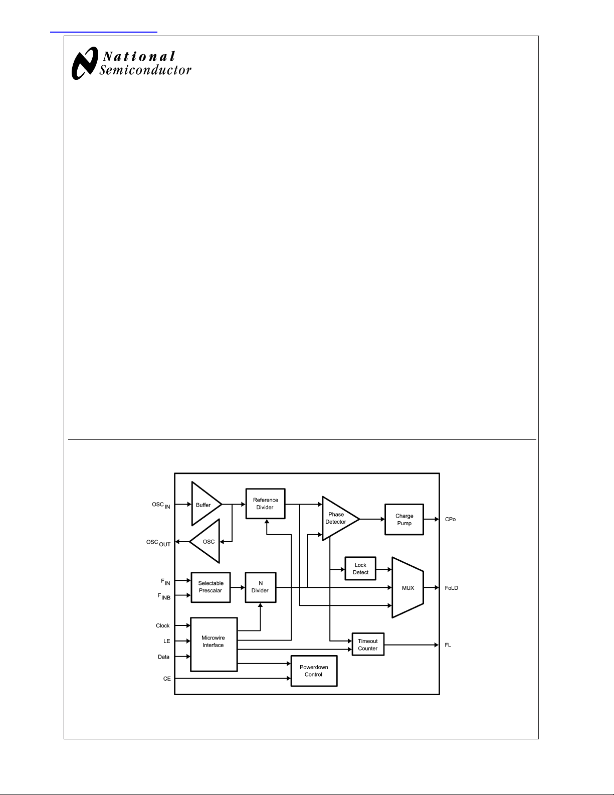
Functional Block Diagram
20043822
PLLatinum™is a trademark of National Semiconductor Corporation.
© 2003 National Semiconductor Corporation DS200438 www.national.com
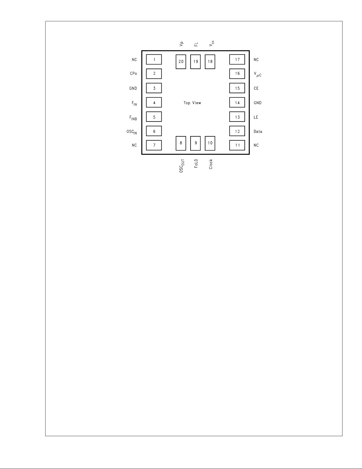
Connection Diagram
LMX2310U/LMX2311U/LMX2312U/LMX2313U
20-Pin Thin Chip Scale Package
NS Package Number SLD20A
20043823
www.national.com 2
Pin Descriptions
Pin Number Pin Name I/O Description I/O Circuit Configuration
1 NC — No Connect.
2CP
o
3 GND — Analog ground.
4F
IN
O Charge Pump output. For connection to a
loop filter for driving the voltage control
input of an external VCO.
I RF prescaler input. Small signal input
from the VCO.
LMX2310U/LMX2311U/LMX2312U/LMX2313U
5F
INB
I RF prescaler complementary input. For
single ended operation, this pin should be
AC grounded. The LMX2310/1/2/3U can
be driven differentially when a bypass
capacitor is omitted.
6 OSC
IN
I Oscillator input. An input to a CMOS low
noise inverting buffer. The input can be
driven from an external CMOS or TTL
logic gate.
7 NC — No Connect.
8 OSC
OUT
O Oscillator output. The OSCINlow noise
buffer drives an independent oscillator
buffer. Its output is connected to the
OSC
pin. It can be used as a buffer to
OUT
provide the reference oscillator frequency
to other circuitry or as a crystal oscillator.
9 FoLD O Multi-function CMOS output pin that
provides multiplexed access to digital lock
detect, open drain analog lock detect, as
well as the outputs of the R and N
counters. The FoLD pin is internally
referenced to V
.
µC
10 Clock I High impedance CMOS Clock input. Data
for the counters is clocked in on the rising
edge, into the 22-bit shift register. The
Clock is internally referenced to V
.
µC
www.national.com3
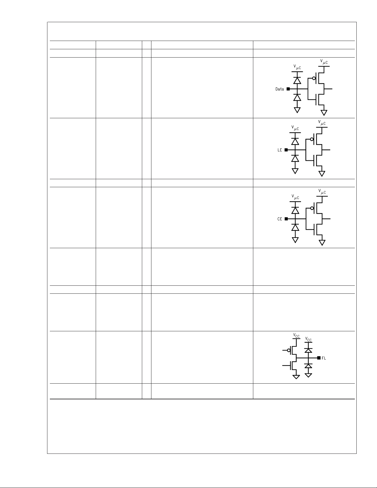
Pin Descriptions (Continued)
Pin Number Pin Name I/O Description I/O Circuit Configuration
11 NC — No Connect.
12 Data I High impedance CMOS Data input. Serial
Data is entered MSB first. The last two
bits are the address for the target
registers. The Data is internally referenced
.
to V
µC
13 LE I High impedance CMOS LE input. When
Latch Enable goes HIGH, data stored in
the 22-bit shift register is loaded into one
the 3 control registers, based on the
LMX2310U/LMX2311U/LMX2312U/LMX2313U
14 GND — Digital ground.
15 CE I High impedance CMOS Chip Enable
address field. The Latch Enable is
internally referenced to V
.
µC
input. Provides logical power-down control
of the device. Pull-up to V
if unused.
µC
The Chip Enable is internally referenced
.
to V
µC
16 V
µC
— Power supply for MICROWIRE™circuitry.
Must be ≤ V
. Typically connected to
CC
same supply level as microprocessor or
baseband controller to enable
programming at low voltages.
17 NC — No Connect.
18 V
CC
— Power supply voltage input. Input may
range from 2.7V to 5.5V. Bypass
capacitors should be placed as close as
possible to this pin and be connected
directly to the ground plane.
19 FL O Fastlock mode output. In Fastlock mode
this pin is at logic low. When not in
Fastlock mode, this pin is in TRI-STATE
mode. This pin can also be forced to
TRI-STATE, forced low or forced high by
the programming of the first two-bits of the
Timeout Counter.
20 V
P
— Power supply for charge pump. Must be ≥
.
V
CC
www.national.com 4
LMX2310U/LMX2311U/LMX2312U/LMX2313U
Absolute Maximum Ratings (Notes 1,
Lead Temp. (solder 4 sec.), (T
) +260˚C
L
2)
If Military/Aerospace specified devices are required,
please contact the National Semiconductor Sales Office/
Distributors for availability and specifications.
Power Supply Voltage,
(V
CC,VP,VµC
) −0.3V to +6.5V
Voltage on any pin with GND=0V
CP
, FL, FIN, OSCIN, OSC
o
Data, Clock, LE, CE, FoLD (V
Storage Temperature Range, (T
) −0.3V to VCC+ 0.3V
OUT(Vi
) −0.3V to VµC+ 0.3V
i
) −65˚C to +150˚C
S
Recommended Operating
Conditions
Power Supply Voltage
(V
) 2.7 5.5 V
CC
(V
)V
P
(V
) 1.72 V
µC
Operating Temperature, (T
(Note 1)
Min Max Unit
5.5 V
CC
CC
) −40 +85 ˚C
A
Electrical Characteristics
VCC=VP=VµC= 3.0V, −40˚C<T
Symbol Parameter Conditions (Note 3) Min Typ Max Units
I
CC
l
CC
I
CC-PWDN
Power Supply
Current
Power-Down Current
RF PRESCALER
F
PF
IN
IN
Operating
Frequency
Input Sensitivity, RF
Prescaler
PHASE DETECTOR
Fφ Phase Detector Frequency 10 MHz
REFERENCE OSCILLATOR
F
OSC
V
OSC
IN
I
IH
I
IL
V
OSC
OUT
D
OSC
OUT
V
OSC
OUT
V
OH
V
OL
I
OH
I
OL
Operating Frequency,
Reference Oscillator Input
Input Sensitivity,
Reference Oscillator Input
OSCINInput Current VIH=VCC= 5.5V 100 µA
OSCINInput Current VIL=0,VCC= 5.5V −100 µA
OSC
OSC
OSC
OSC
OSC
OSC
OSC
Bias Level OSCINOpen 1.5 V
OUT
Duty Cycle
OUT
Level
OUT
Output Voltage IOH= -500 µA 2.6 2.8 V
OUT
Output Voltage IOL= 500 µA 0.2 0.4 V
OUT
Output Current VOH= 2.25 V -1.1 mA
OUT
Output Current VOL= 0.75 V 1.1 mA
OUT
<
+85˚C unless specified otherwise.
A
LMX2310U
LMX2311U
LMX2312U
LMX2313U
(Note 4) 2.3 3.0 mA
V
= 5.5V (Note 4) 3.4 mA
CC
(Note 4) 2.0 2.7 mA
V
= 5.5V (Note 4) 3.2 mA
CC
(Note 4) 1.4 2.0 mA
V
= 5.5V (Note 4) 2.4 mA
CC
(Note 4) 1.0 1.3 mA
V
= 5.5V (Note 4) 1.6 mA
CC
Clock, Data and LE = GND
CE = GND
110 µA
LMX2310U 0.5 2.5 GHz
LMX2311U 0.5 2.0 GHz
LMX2312U 0.2 1.2 GHz
LMX2313U 45 600 MHz
2.7 ≤ V
3.0V
≤3.0V (Note 5) −15 0 dBm
CC
<
VCC≤ 5.5V (Note 5) −10 0 dBm
2 50 MHz
(Note 6) 0.5 V
OSC
= 20 MHz, 0.5 V
IN
Duty Cycle = 50%
OSC
IN
OSC
= 20 MHz, 0.5 V
IN
OSC
OUT
Load=10pF||10k
P-P
P-P
,
50 %
,
2.6 V
CC
V
P−P
P-P
Ohm
V
www.national.com5
Electrical Characteristics (Continued)
VCC=VP=VµC= 3.0V, −40˚C<T
Symbol Parameter Conditions (Note 3) Min Typ Max Units
CHARGE PUMP
ICPo-
source
ICPo-
ICPo-
ICPo-
ICPo-
sink
source
sink
tri
Charge Pump Output
Current (Note 7)
Charge Pump TRI-STATE
Current
vs.
ICPoICPo-
sink
source
CP Sink vs. Source
Mismatch
ICPo vs VCPo CP Current vs. Voltage 0.5V ≤ VCPo ≤ V
ICPo vs T
LMX2310U/LMX2311U/LMX2312U/LMX2313U
CP Current vs.
A
Temperature
DIGITAL INTERFACE (Data, Clock, LE, CE)
V
IH
V
IL
I
IH
I
IL
V
OH
High-level Input Voltage VµC= 1.72V to 5.5V 0.8 V
Low-level Input Voltage VµC= 1.72V to 5.5V 0.2 V
High-level Input Current VIH=VµC= 5.5V −1.0 1.0 µA
Low-level Input Current VIL= 0V, VµC= 5.5V −1.0 1.0 µA
High-level Output Voltage
(Pin 7– FoLD)
High-level Output Voltage
(Pin 15– FL)
V
OL
Low-level Output Voltage IOL= 1.0 mA (Note 9) 0.1 0.4 V
MICROWIRE TIMING (Data, Clock, LE, CE)
t
CS
t
CH
t
CWH
t
CWL
t
ES
Data to Clock Set Up Time (Note 10) 50 ns
Data to Clock Hold Time (Note 10) 20 ns
Clock Pulse Width High (Note 10) 50 ns
Clock Pulse Width Low (Note 10) 50 ns
Clock to Load Enable Set
Up Time
t
EW
Load Enable Pulse Width (Note 10) 50 ns
<
+85˚C unless specified otherwise.
A
VCPo = Vp/2, ICPo_4X = 0 0.8 1.0 1.2 mA
VCPo = Vp/2, ICPo_4X = 0 −0.8 −1.0 −1.2 mA
VCPo = Vp/2, ICPo_4X = 1 3.2 4.0 4.8 mA
VCPo = Vp/2, ICPo_4X = 1 −3.2 −4.0 −4.8 mA
0.5V ≤ VCPo ≤ VP− 0.5V
−2.5 2.5 nA
VCPo = Vp/2
T
A
= 25˚C
310 %
(Note 8)
− 0.5V
P
= 25˚C (Note 8)
T
A
VCPo = Vp/2V (Note 7)
IOH= 500 µA
I
= −500 µA
OH
(Note 10)
µC
− 0.4 V
V
µC
− 0.4 V
V
CC
50 ns
815 %
8%
V
µC
V
www.national.com 6
Electrical Characteristics (Continued)
VCC=VP=VµC= 3.0V, −40˚C<T
Symbol Parameter Conditions (Note 3) Min Typ Max Units
PHASE NOISE CHARACTERISTICS
L
L(f)
(f)
N
Normalized Single
Side-Band Phase Noise
Single Side-Band Phase
Noise
<
+85˚C unless specified otherwise.
A
= 200 kHz
F
φ
=10MHz
F
OSC
= 1.0 V
V
OSC
PP
ICPO=4mA
= 25˚C
T
A
(Note 11)
LMX2310U
= 2450 MHz
F
IN
= 200 kHz
F
φ
=10MHz
F
OSC
= 1.0 V
V
OSC
PP
ICPO=4mA
= 25˚C
T
A
(Note 12)
LMX2311U
= 1960 MHz
F
IN
= 200 kHz
F
φ
=10MHz
F
OSC
= 1.0 V
V
OSC
PP
ICPO=4mA
= 25˚C
T
A
(Note 12)
LMX2312U
= 902 MHz
F
IN
= 200 kHz
F
φ
=10MHz
F
OSC
= 1.0 V
V
OSC
PP
ICPO=4mA
= 25˚C
T
A
(Note 12)
LMX2313U
= 450 MHz
F
IN
=50kHz
F
φ
=10MHz
F
OSC
= 1.0 V
V
OSC
PP
ICPO=4mA
= 25˚C
T
A
(Note 12)
−159 dBc/Hz
−78 dBc/Hz
−80 dBc/Hz
−85 dBc/Hz
−85 dBc/Hz
LMX2310U/LMX2311U/LMX2312U/LMX2313U
Note 1: Absolute Maximum Ratings indicate limits beyond which damage to the device may occur. Operating Ratings indicate conditions for which the device is
intended to be functional, but do not guarantee specific performance limits. For guaranteed specifications and conditions, see the Electrical Characteristics. The
guaranteed specifications apply only for the conditions listed.
Note 2: This device is a high performance RF integrated circuit with an ESD rating
workstations.
Note 3: Typical Conditions are at a T
Note 4: Icc current is measured with Clock, Data and LE pins connected to GND. OSCin and Fin pins are connected to Vcc. PWDN bit is program to 0. Icc current
is the current into Vcc pin.
Note 5: See F
Note 6: See OSC
Note 7: Charge Pump Magnitude is controlled by CPo_4X bit [R18].
Note 8: See Charge Pump Measurement Definition for detail on how these measurements are made.
Note 9: Analog Lock Detect open drain output pin only can be pulled up to V
Note 10: See Serial Input Data Timing.
Note 11: Normalized Single-Side Band Phase Noise is defined as: L
Sensitivity Test Setup.
IN
Sensitivity Test Setup.
IN
of 25˚C.
A
(f) = L(f) − 20 log (FIN/Fφ), where L(f) is defined as the Single Side-Band Phase Noise.
N
<
2 kV. Handling and assembly of this device should only be done at ESD free
that will not exceed 6.5V.
ext
www.national.com7
Note 12: Phase Noise is measured using a reference evaluation board with a loop bandwidth of approximately 12 kHz. The phase noise specification is the
composite average of 3 measurements made at frequency offsets of 2.0 kHz, 2.5 kHz and 3.0 kHz.
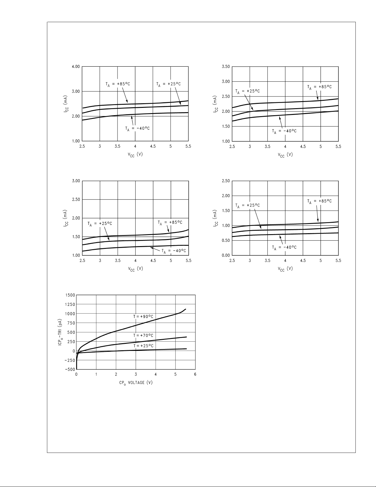
Typical Performance Characteristics
Iccvs VccLMX2310U Iccvs VccLMX2311U
LMX2310U/LMX2311U/LMX2312U/LMX2313U
20043838
Iccvs VccLMX2312U Iccvs VccLMX2313U
20043839
CPOTRI-STATE vs CPOVoltage
20043840 20043841
20043843
www.national.com 8
Typical Performance Characteristics (Continued)
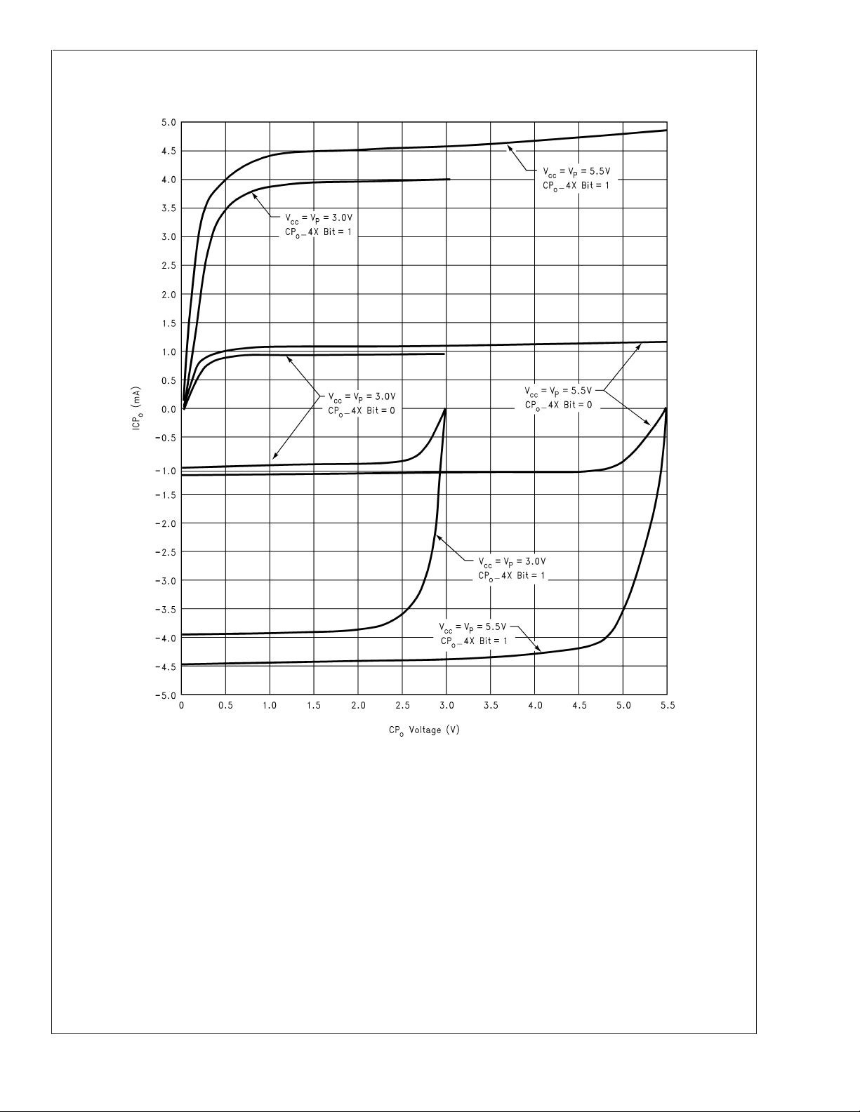
LMX231xU Charge Pump Sweeps
LMX2310U/LMX2311U/LMX2312U/LMX2313U
20043842
www.national.com9

Typical Performance Characteristics (Continued)
Charge Pump Current Variation (See formula under
Charge Pump Current Specification Definitions)
LMX2310U/LMX2311U/LMX2312U/LMX2313U
Sink Vs Source Mismatch (See formula under Charge
Pump Current Specification Definitions)
20043866
LMX2310U FinSensitivity vs Frequency at 3.0V
20043867
www.national.com 10
20043846

Typical Performance Characteristics (Continued)
LMX2310U/LMX2311U/LMX2312U/LMX2313U
LMX2310U F
Sensitivity vs Frequency at 5.5V
in
LMX2311U FinSensitivity vs Frequency at 3.0V
20043847
20043848
www.national.com11

Typical Performance Characteristics (Continued)
LMX2310U/LMX2311U/LMX2312U/LMX2313U
LMX2311U F
Sensitivity vs Frequency at 5.5V
in
LMX2312U FinSensitivity vs Frequency at 3.0V
20043849
www.national.com 12
20043850

Typical Performance Characteristics (Continued)
LMX2310U/LMX2311U/LMX2312U/LMX2313U
LMX2312U F
Sensitivity vs Frequency at 5.5V
in
LMX2313U FinSensitivity vs Frequency at 3.0V
20043851
20043852
www.national.com13

Typical Performance Characteristics (Continued)
LMX2310U/LMX2311U/LMX2312U/LMX2313U
LMX2313U F
Sensitivity vs Frequency at 5.5V
in
LMX231XU OSCinSensitivity vs Frequency at 3.0V
20043853
www.national.com 14
20043854

Typical Performance Characteristics (Continued)
LMX2310U/LMX2311U/LMX2312U/LMX2313U
LMX231XU OSC
Sensitivity vs Frequency at 5.5V
in
LMX231xU OSCinInput Impedance vs Frequency
20043855
20043858
www.national.com15

Typical Performance Characteristics (Continued)
LMX231xUSLD OSCINIMPEDANCE
V
= 3.0V (TA= 25˚C) VCC= 5.5V (TA= 25˚C)
CC
OSC
BUFFER
IN
NORMAL OPERATION
F
OSC
(MHz)
Real
ZOSC
(Ω)
IN
Imag-
inary
ZOSC
(Ω)
IN
|ZOSC
(Ω)
|
IN
2 12900 −1500 13000 9000 −33000 34200 10000 −7400 12400 12000 −35000 37000
4 5200 −10900 12100 2000 −20000 20100 5500 −7800 9500 12200 −21000 24300
7 2400 −7500 7900 1100 −13000 13000 2700 −5700 6300 1300 −13000 13100
10 1350 −5400 5600 410 −9500 9500 1600 −4500 4800 800 −9100 9100
13 920 −4300 4400 350 −7000 7000 1000 −3500 3600 300 −7800 7800
16 820 −3600 3700 450 −5900 5900 800 −3900 4000 400 −6000 6000
LMX2310U/LMX2311U/LMX2312U/LMX2313U
19 630 −3100 3200 220 −5000 5000 630 −2500 2600 310 −5100 5100
22 570 −2600 2700 200 −4300 4300 540 −2100 2200 280 −4400 4400
25 420 −2100 2100 150 −3800 3800 450 −1900 2000 180 −3900 3900
28 440 −2000 2000 140 −3400 3400 400 −1700 1700 140 −3500 3500
31 390 −1900 1900 140 −3000 3000 350 −1500 1500 120 −3100 3100
34 360 −1800 1800 80 −2700 2700 330 −1400 1440 110 −2900 2900
37 340 −1700 1700 100 −2500 2500 310 −1300 1340 100 −2600 2600
40 330 −1500 1500 100 −2400 2400 300 −1200 1240 120 −2400 2400
43 300 −1400 1400 95 −2200 2200 280 −1100 1140 100 −2300 2300
46 290 −1400 1400 80 −2100 2100 270 −1000 1040 90 −2100 2100
49 280 −1300 1300 70 −1900 1900 260 −1000 1030 80 −2000 2000
50 280 −1300 1300 70 −1900 1900 260 −990 1020 100 −2000 2000
OSCINBUFFER
POWERED-DOWN MODE
IN
Imag-
inary
ZOSC
(Ω)
IN
|ZOSC
(Ω)
Real
ZOSC
(Ω)
OSCINBUFFER
NORMAL OPERATION
Real
|
IN
ZOSC
IN
ZOSC
(Ω)
Imag-
inary
(Ω)
IN
|ZOSC
(Ω)
OSCINBUFFER
POWERED-DOWN MODE
IN
Imag-
inary
ZOSC
(Ω)
Real
|
IN
ZOSC
(Ω)
IN
|ZOSC
(Ω)
|
IN
www.national.com 16

Typical Performance Characteristics (Continued)
LMX2310U/LMX2311U/LMX2312U/LMX2313U
LMX231xU F
Input Impedance vs Frequency
in
=3.0V, TA= 25˚C
V
CC
LMX231xU FinInput Impedance vs Frequency
=5.5V, TA= 25˚C
V
CC
20043856
20043857
www.national.com17

Typical Performance Characteristics (Continued)
LMX231xUSLD FINIMPEDANCE
V
= 3.0V (TA= 25˚C) VCC= 5.5V (TA= 25˚C)
CC
F
IN
F
IN
(MHz)
POWERED-UP
Real
ZF
IN
(Ω)
Imaginary
ZF
IN
(Ω)
|ZF
(Ω)
IN
POWERED-DOWN
Real
|
ZF
IN
(Ω)
100 452 −325 557 440 −337 554 460 −325 563 444 −333 555
200 305 −278 413 300 −276 408 313 −277 418 312 −275 416
300 225 −243 331 225 −242 330 235 −244 339 237 −244 340
400 180 −219 283 179 −217 281 190 −221 291 189 −221 291
500 147 −197 246 145 −195 243 155 −200 253 155 −200 253
600 120 −175 212 118 −173 209 127 −179 219 126 −179 219
700 102 −158 188 100 −156 185 108 −162 195 107 −161 193
LMX2310U/LMX2311U/LMX2312U/LMX2313U
800 88 −141 166 86 −139 163 94 −146 174 91 −143 169
900 78 −126 148 75 −123 144 83 −131 155 81 −129 152
1000 73 −117 138 72 −113 134 78 −118 141 75 −116 138
1100 64 −109 126 63 −106 123 69 −112 132 68 −111 130
1200 57 −98 113 55 −95 110 61 −102 119 59 −100 116
1300 52 −90 104 52 −86 100 55 −95 110 55 −91 106
1400 46 −84 96 46 −83 95 49 −88 101 50 −87 100
1500 41 −75 85 40 −73 83 44 −79 90 42 −78 89
1600 39 −69 79 37 −66 76 41 −73 84 40 −70 81
1700 35 −61 70 34 −59 68 37 −65 75 36 −63 73
1800 34 −55 65 33 −52 62 35 −58 68 34 −56 66
1900 35 −50 61 35 −47 59 35 −52 63 35 −50 61
2000 37 −50 62 37 −48 61 38 −50 63 38 −48 61
2100 34 −52 62 33 −51 61 36 −52 63 34 −51 61
2200 29 −50 58 27 −48 55 32 −51 60 30 −50 58
2300 25 −48 54 23 −45 51 27 −50 57 25 −48 54
2400 20 −44 48 19 −42 46 23 −47 52 21 −44 49
2500 18 −41 45 16 −38 41 20 −43 47 18 −41 45
F
IN
Imaginary
ZF
IN
(Ω)
|ZF
(Ω)
F
IN
POWERED-UP
Real
ZF
(Ω)
IN
Imaginary
ZF
IN
(Ω)
|
IN
|ZF
IN
(Ω)
POWERED-DOWN
Real
|
ZF
IN
(Ω)
F
IN
Imaginary
ZF
IN
(Ω)
|ZF
(Ω)
|
IN
www.national.com 18

Charge Pump Measurement Definitions
LMX2310U/LMX2311U/LMX2312U/LMX2313U
I1=CPosink current at VCPo=VP− ∆V
sink current at VCPo=VP/2
I2=CP
o
sink current at VCPo= ∆V
I3=CP
o
source current at VCPo=VP− ∆V
I4=CP
o
source current at VCPo=VP/2
I5=CP
o
source current at VCPo= ∆V
I6=CP
o
∆V = 0.5V
Charge Pump Output Current Magnitude Variation Vs Charge Pump Output Voltage
Charge Pump Output Current Sink Vs Charge Pump Output Current Source Mismatch
Charge Pump Output Current Magnitude Variation Vs Temperature
20043837
20043863
20043864
20043865
www.national.com19

Serial Data Input Timing
Notes:
1. Data shifted into register on Clock rising edge.
LMX2310U/LMX2311U/LMX2312U/LMX2313U
2. Data is shifted in MSB first.
FINSensitivity Test Setup
20043810
Notes:
1. LMX2310/1/2U Test Conditions: NA_CNTR = 16, NB_CNTR = 312,P=1,FoLD2 = 1, FoLD1 = 1, FoLD0 = 0, PWDN = 0.
2. LMX2313U Test Conditions: NA_CNTR = 0, NB_CNTR = 625,P=1,FoLD2 = 1, FoLD1 = 1, FoLD0 = 0, PWDN = 0.
3. Sensitivity limit is reached when the frequency error of the divided RF input is greater than or equal to 1 Hz.
www.national.com 20
20043830

OSCINSensitivity Test Setup
LMX2310U/LMX2311U/LMX2312U/LMX2313U
Notes:
1. Test Conditions: R_CNTR = 1000, FoLD2 = 1, FoLD1 = 0, FoLD0 = 1, PWDN = 0.
2. Sensitivity limit is reached when the frequency error of the divided RF input is greater than or equal to 1 Hz.
20043831
www.national.com21

1.0 Functional Description
The basic phase-lock-loop (PLL) configuration consists of a
high-stability crystal reference oscillator, a frequency synthesizer such as the National Semiconductor LMX2310/1/2/3U,
a voltage controlled oscillator (VCO), and a passive loop
filter. The frequency synthesizer includes a phase detector, a
current mode charge pump, as well as a programmable
reference divider and feedback frequency divider. The VCO
frequency is established by dividing the crystal reference
signal down via the reference divider to obtain a frequency
that sets the comparison frequency. This reference signal, f
is then presented to the input of a phase/frequency detector
and compared with another signal, f
LMX2310U/LMX2311U/LMX2312U/LMX2313U
, which was obtained by
p
dividing the VCO frequency down by way of the feedback
counter. The phase/frequency detector measures the phase
error between the f
and fpsignals and outputs control sig-
r
nals that are directly proportional to the phase error. The
charge pump then pumps charge into or out of the loop filter
based on the magnitude and direction of the phase error.
The loop filter converts the charge into a stable control
voltage for the VCO. The phase/frequency detector’s function is to adjust the voltage presented to the VCO until the
feedback signal’s frequency and phase match that of the
,
r
reference signal. When this “phase-locked” condition exists,
the RF VCO frequency will be N times that of the comparison
frequency, where N is the feedback divider ratio.
20043829
1.1 REFERENCE OSCILLATOR
The reference oscillator frequency for the RF PLL is provided
from the external source via the OSC
pin. The low noise
in
reference buffer circuit supports frequencies from 2 MHz to
50 MHz with a minimum input sensitivity of 0.5 V
. The input
pp
can be driven from an external CMOS or TTL logic gate. The
output of this buffer drives the R COUNTER. The output of
the buffer also connects to an oscillator/buffer circuit. Its
output connects to the OSC
pin. The oscillator/buffer cir-
out
cuit can be used as a buffer to provide the reference frequency to other circuitry. It can also be used as an oscillator
with a crystal/resonator with proper components connected
between OSC
and OSC
in
pins to generate a reference
out
frequency.
1.2 REFERENCE DIVIDER (R COUNTER)
The reference divider is comprised of a 15-bit CMOS binary
counter that supports a continuous integer divide range from
2 to 32,767. The divide ratio should be chosen such that the
maximum phase comparison frequency of 10 MHz is not
exceeded. The reference divider circuit is clocked by the
output of the reference buffer circuit. The output of the
reference divider circuit feeds the reference input of the
phase detector circuit. The frequency of the reference input
to the phase detector (also referred to as the comparison
frequency) is equal to reference oscillator frequency divided
by the reference divider ratio. Refer to Section 3.2.1 for
details on programming the R COUNTER.
1.3 PRESCALERS
The LMX2310/1/2U contains a selectable, dual modulus
32/33 and 16/17 prescaler. The LMX2313U contains a selectable, dual modulus 16/17 and 8/9 prescaler.
PLL
Input
Frequency
>
1.2 GHz LMX2310/1U 32/33
F
IN
PLL
Part
Numbers
Allowable
Prescaler
Values
PLL
Input
Frequency
≤ 1.2 GHz LMX2310/1/2U 16/17 or
F
IN
PLL
Part
Numbers
Allowable
Prescaler
Values
32/33
≤ 600
F
IN
MHz
The complimentary F
LMX2313U 8/9 or
IN
and F
input pins drive the input of
INB
16/17
a bipolar, differential-pair amplifier. The output of the bipolar,
differential-pair amplifier drives a chain of ECL D-type flipflops in a dual modulus configuration. The output of the
prescaler is used to clock the subsequent programmable
feedback divider. Refer to Section 3.3.2 for details on programming the Prescaler Value.
1.4 FEEDBACK DIVIDER (N COUNTER)
The N COUNTER is clocked by the output of the prescaler.
The N COUNTER is composed of a 13-bit programmable
integer divider. The 5-bit swallow counter is part of the
prescaler. Selecting a 32/33 prescaler provides a minimum
continuous divider range from 992 to 262,143 while selecting
a 16/17 prescaler value allows for continuous divider values
from 240 to 131,071. In the LMX2313U, selecting a 8/9
prescaler provides a minimum continuous divider range from
56 to 65535.
N = (P x NB_CNTR) + NA_CNTR
F
=NxF
IN
φ
Definitions
F
φ
F
IN
Phase Detector Comparison Frequency
RF Input Frequency
P Prescaler Value
NA_CNTR A Counter Value
NB_CNTR B Counter Value
www.national.com 22

1.0 Functional Description (Continued)
1.5 PHASE/FREQUENCY DETECTORS
The phase/frequency detector is driven from the N and R
COUNTER outputs. The maximum frequency at the phase
detector inputs is 10 MHz. The phase detector outputs con-
Phase Comparator and Internal Charge Pump Characteristics
LMX2310U/LMX2311U/LMX2312U/LMX2313U
trol the charge pump. The polarity of the pump-up or pumpdown control signals are programmed using the PD_POL
control bit, depending on whether the RF VCO tuning characteristics are positive or negative (see programming description in Section 3.2.2). The phase/frequency detector
has a detection range of −2π to +2π.
Note 13: The minimum width of the pump up and pump down current pulses occur at the CPopin when the loop is phase-locked.
Note 14: The diagram assumes that PD_POL = 1
Note 15: f
Note 16: f
Note 17: CP
1.6 CHARGE PUMP
The charge pumps directs charge into or out of an external
loop filter. The loop filter converts the charge into a stable
control voltage which is applied to the tuning input of a VCO.
The charge pump steers the VCO control voltage towards V
during pump-up events and towards GND during pumpdown events. When locked, CP
condition with small corrections occurring at the phase comparison rate. The charge pump output current magnitude can
be selected as 1.0 mA or 4.0 mA by programming the
ICPo_4X bits. When TO_CNTR[11:0] = 1, the charge pump
output current magnitude is set to 4.0 mA. Refer to Section
3.2.3 and 3.4.2 for details on programming the charge pump
output current magnitude.
is the phase comparator input from the R Divider
r
is the phase comparator input from the N Divider
p
is charge pump output
o
is primarily in a TRI-STATE
o
ence divider and the feedback divider circuits. The FoLD
output pin is referenced to the V
FoLD1 and FoLD2 bits are used to select the desired output
function. A complete programming description of the FoLD
P
output pin is in Section 3.2.5.
1.8.1 Analog Lock Detect
When programmed for analog lock detect, the analog lock
detect status is available on the FoLD output pin. When the
charge pump is inactive, the lock detect output goes to a
high impedance in the open drain configuration and to a V
source in a push-pull configuration. It goes low when the
charge pump is active during a comparison cycle. The analog lock detect status can be programmed in either an open
drain or push-pull configuration. The push-pull output is ref-
1.7 MICROWIRE SERIAL INTERFACE
The programmable register set is accessed through the
MICROWIRE serial interface. The interface is comprised of
three signal pins: CLOCK, DATA and LE (Latch Enable). The
MICROWIRE circuitry is referenced to V
, which allows the
µC
circuitry to operate down to a 1.72V source. Serial data is
clocked into a 22-bit shift register from DATA on the rising
edge of CLOCK. The serial data is clocked in MSB first. The
last two bits decode the internal register address. On the
rising edge of LE, the data stored in the shift register is
loaded into one of the three latches based on the address
bits. The synthesizer can be programmed even in the powerdown state. A complete programming description is in Section 3.0.
erenced to V
1.8.2 Digital Lock Detect
When programmed for digital lock detect, the digital lock
detect status is available on the FoLD pin. The digital lock
detect filter compares the phase difference of the inputs from
the phase detector to a RC generated delay of approximately 15 ns. To enter the locked state (LD = High), the
phase error must be less than the 15 ns RC delay for 5
consecutive reference cycles. Once in lock, the RC delay is
changed to approximately 30 ns. To exit the locked state, the
phase error must be greater than the 30 ns RC delay. When
a PLL is in power-down mode, the respective lock detect
output is always low. A flow chart of the digital lock detect
.
µC
filter follows:
1.8 MULTI-FUNCTION OUTPUTS
The LMX2310/1/2/3U FoLD output pin is a multi-function
output that can be configured as an analog lock detect, a
digital lock detect, and a monitor of the output of the refer-
20043804
supply. The FoLD0,
µC
µC
www.national.com23

1.0 Functional Description (Continued)
LMX2310U/LMX2311U/LMX2312U/LMX2313U
1.9 Fastlock™OUTPUT
The FL pin can be used as the Fastlock output. The FL pin
can also be programmed as constant low, constant high
(referenced to V
), or constant high impedance, selectable
CC
through the T register. When the device is configured in
Fastlock mode, the charge pump current can be increased
4x while maintaining loop stability by synchronously switching a parallel loop filter resistor to ground with the FL pin,
resulting in a ∼2x increase in loop bandwidth. The loop
bandwidth, the zero gain crossover point of the open loop
gain, is effectively shifted up in frequency by a factor of the
square root of 4 = 2 during Fastlock mode. For ω'=2ω, the
phase margin during Fastlock also will remain constant. The
user calculates the loop filter component values for the
normal steady state considerations. The device configuration ensures that as long as a second resistor, equal to the
primary resistor value, is wired in appropriately, the loop will
lock faster without any additional stability considerations.
www.national.com 24
20043805
The PLL can be configured to be in either the Fastlock mode
continuously or in the Fastlock mode that uses a timeout
counter to switch it back to the normal mode. In the Fastlock
mode the charge pump current is set to 4 mA and the FL pin
is set low. If the user sets the PLL to be in the Fastlock mode
continuously he can send the R register with CPo_4X set low
(R[18] = 0) and sets TO_CNTR[11:0] to 1. The user can set
the PLL to normal mode (1 mA mode and set the FL pin to
TRI-STATE mode) by programming TO_CNTR[11:0] to 0. If
the user elects to use the timeout counter, he can program
the timeout counter from 4 to 4095. The timeout counter will
count down the programmed number of phase detector reference cycles. After the programmed number of phase detector reference cycles is reached, it will automatically set
the charge pump current to the 1 mA mode and set the FL
pin to TRI-STATE mode. A complete programming description is in Section 3.4.2.

2.0 Power-Down
The LMX2310/1/2/3U are power controlled through logical
control of the CE pin in conjunction with programming of the
PDWN and CPo_TRI bits. A truth table is provided that
describes how the state of the CE pin, the PDWN bit and
CPo_TRI bit set the operating mode of the device. A complete programming description of Power-Down is provided in
Section 3.3.1.
CE PWDN CPo_TRI Operating Mode
0 X X Power-down (Asynchronous)
1 0 0 Normal Operation
1 1 0 Power-down (Synchronous)
1 1 1 Power-down (Asynchronous)
X = Don’t Care
When the device enters the power-down mode, the oscillator
buffer, RF prescaler, phase detector, and charge pump circuits are all disabled. The OSC
are all forced to a high impedance state. The reference
divider and feedback divider circuits are disabled and held at
, CPo, FIN,F
IN
, LD pins
INB
the load point during power-down. When the device is programmed to normal operation, the oscillator buffer, RF prescaler, phase detector, and charge pump circuits are all powered on. The feedback divider and the reference divider are
held at the load point. This allows the RF prescaler, feedback
divider, reference oscillator, the reference divider and prescaler circuitry to reach proper bias levels. After a 1.5 µs
delay, the feedback and reference divider are enabled and
they resume counting in “close” alignment (The maximum
error is one prescaler cycle). The MICROWIRE control register remains active and capable of loading and latching in
data while in the power-down mode.
The synchronous power-down function is gated by the
charge pump. When the device is configured for synchronous power-down, the device will enter the power-down
mode upon the completion of the next charge pump pulse
event.
The asynchronous power-down function is NOT gated by the
completion of a charge pump pulse event. When the device
is configured for asynchronous power-down, the part will go
into power-down mode immediately.
3.0 Programming Description
3.1 MICROWIRE INTERFACE
The MICROWIRE interface is comprised of a 22-bit shift register and three control registers. The shift register consists of a 20-bit
DATA field and a 2-bit address (ADDR) field as shown below. Data is loaded into the shift register on the rising edges of the
CLOCK signal MSB first. When Latch Enable transitions HIGH, data stored in the shift register is loaded into either the R, N or
T register depending on the state of the ADDR bit. The DATA field assignments for the R, N and T registers are shown in Section
3.1.1.
MSB LSB
DATA ADDRESS
21 2 0
LMX2310U/LMX2311U/LMX2312U/LMX2313U
ADDR Target Register
0 R register
1 N register
2 T register
3.1.1 Register Map
Register Most Significant Bit SHIFT REGISTER BIT LOCATION Least Significant Bit
21 20 19 18 17 1615 14 1312111098765432 1 0
Data Field
R FoLD1 FoLD0
N PWDN P B_CNTR[12:0] A_CNTR[4:0] 0 1
T 0 0 0 0 0 0 0 FoLD2 TO_CNTR[11:0] 1 0
CPo_
TRI
CP0_4xPD_
POL
R_CNTR[14:0] 0 0
Address
Field
www.national.com25

3.0 Programming Description (Continued)
3.2 R REGISTER
The R register contains the R_CNTR control word and PD_POL, CPo_4X, CP_TRI, FoLD0, FoLD1 control bits. The detailed
descriptions and programming information for each control word is discussed in the following sections.
Register Most Significant Bit SHIFT REGISTER BIT LOCATION Least Significant Bit
21 20 19 18 17 1615141312111098765432 1 0
Data Field
R FoLD1 FoLD0 CP
3.2.1 R_CNTR[14:0] Reference Divider (R COUNTER) R[16:2]
The reference divider can be programmed to support divide ratios from 2 to 32,767. Divide ratios of less than 2 are prohibited.
Divider Value R_CNTR[14:0]
LMX2310U/LMX2311U/LMX2312U/LMX2313U
2 000000000000010
3 000000000000011
• •••••••••••••••
32,767 111111111111111
3.2.2 PD_POL Phase Detector Polarity R[17]
The PD_POL control bit is used to set the polarity of the phase detector based on the VCO tuning characteristic.
TRI
_
O
CPO_4XPD_
POL
R_CNTR[14:0] 0 0
Address
Field
Control Bit Register Location Description
01
Function
PD_POL R[17] Phase Detector Polarity Negative VCO Tuning Characteristic Positive VCO Tuning Characteristic
VCO Characteristics
20043809
3.2.3 CPo_4X Charge Pump Output Current R[18]
The CPo_4X control bit allows the charge pump output current magnitude to be switched from 1 mA to 4 mA. This happens
asynchronously or immediately with the change in CPo_4X bit.
Control Bit Register Location Description
Function
01
CPo_4X R[18] Charge Pump Output Current Magnitude 1X Current 4X Current
3.2.4 CPo_TRI Charge Pump TRI-STATE R[19]
The CPo_TRI control bit allows the charge pump to be switched between a normal operating mode and a high impedance output
state. This happens asynchronously or immediately with the change in CPo_TRI bit.
Control Bit Register Location Description
01
Function
CPo_TRI R[19] Charge Pump TRI-STATE Charge Pump Operates Normal Charge Pump Output in High
Impedance State
www.national.com 26

3.0 Programming Description (Continued)
3.2.5 FoLD2,1,0 FoLD Output Truth Table T[14],R[21],R[20]
The FoLD2, FoLD1 and FoLD0 are used to select which signal is routed to FoLD pin.
LMX2310U/LMX2311U/LMX2312U/LMX2313U
T[14] R[21] R[20]
FoLD2 FoLD1 FoLD0
FoLD Output State
0 0 0 Disabled (TRI-STATE FoLD)
0 0 1 Lock Detect —Analog (Push/Pull), Reference to V
µc
0 1 0 Lock Detect —Analog (Open Drain)
0 1 1 Reset R and N Dividers and TRI-STATE Charge Pump
1 0 0 Lock Detect —Digital (Push/Pull), Reference to V
1 0 1 R COUNTER Output (Push/Pull), Reference to V
1 1 0 N Counter Output (Push/Pull), Reference to V
µC
µC
µC
1 1 1 Reserved (Do Not Use)
3.3 N REGISTER
The N register contains the PWDN (Power-Down), P (Prescaler), NA_CNTR, and NB_CNTR control words. The detailed
descriptions and programming information for each control word is discussed in the following sections.
Register Most Significant Bit SHIFT REGISTER BIT LOCATION Least Significant Bit
21 201918171615141312111098765432 1 0
Data Field
Address
Field
N PWDN P B_CNTR[12:0] A_CNTR[4:0] 0 1
3.3.1 PWDN Power-Down N[21]
The PWDN control bit along with CP
or asynchronous powered down by first setting the CP
Power-Down mode, the CP
_TRI bit will have to be reset to 0.
o
_TRI control bit is used to power-down the PLL. The LMX2310/1/2/3U can be synchronous
o
N[21] R[19]
PWDN CP
_TRI bit and then setting the PWDN bit. To power up from the synchronous
o
O
_TRI
Operating Mode
0 0 Normal Operation
1 0 Power-down (Synchronous)
1 1 Power-down (Asynchronous)
3.3.2 P Prescaler N[20]
The LMX2310/1/2/3U contains two dual modulus prescalers. The P control bit is used to set the prescaler value.
N[20]
Prescaler Value
LMX2310/1/2U
Prescaler Value
LMX2313U
0 16/17 8/9
1 32/33 16/17
PLL Input Frequency Allowable Prescaler Values
>
F
1.2 GHz 32/33
IN
F
≤ 1.2 GHz 16/17 or 32/33
IN
F
≤ 600 MHz 8/9 or 16/17
IN
www.national.com27

3.0 Programming Description (Continued)
3.3.3 B_CNTR[12:0] B COUNTER N[19:7]
The NB_CNTR control word is used to program the B counter. The B counter is a 13-bit binary counter used in the programmable
feedback divider. The B counter can be programmed to values ranging from 3 to 8,191. See Section 1.4 for details on how the
value of the B counter should be selected.
Divider Value B_CNTR[12:0]
3 0000000000011
4 0000000000101
• •••••••••••••
8,191 1111111111111
NOTE: B counter divide ratio must be ≥ 3.
3.3.4 A_CNTR[4:0] A Counter N[6:2]
The NA_CNTR control word is used to program the A counter. The A counter is a 5-bit swallow counter used in the programmable
feedback divider. The A counter can be programmed to values ranging from 0 to 31. See Section 1.4 for details on how the value
of the A counter should be selected.
LMX2310U/LMX2311U/LMX2312U/LMX2313U
Divide
Ratio
A_CNTR[4:0]
000000
100001
••••••
3111111
NOTES: A counter divide ratio must be ≤ P and A counter divide ratio must be ≤ B counter divide ratio.
3.4 T REGISTER
The T register contains the TO_CNTR control word and FoLD2 control bit. The detailed descriptions and programming
information for each control word is discussed in the following sections.
Register Most Significant Bit SHIFT REGISTER BIT LOCATION Least Significant Bit
21201918171615 14 1312111098765432 1 0
Data Field
Address
Field
T 0000000FoLD2 TO_CNTR[11:0] 1 0
3.4.1 FoLD2 FoLD Output (P/O Output Truth Table) T[14]
See Section 3.2.5 for FoLD Output Truth Table details.
3.4.2 TO_CNTR[11:0] Timeout Counter Table T[13:2]
When the Fastlock Timeout counter (TO_CNTR) is loaded with 0, Fastlock is off, the FL pin will be in TRI-STATE mode, and the
charge pump current will be the value specified by the Charge Pump Magnitude bit, R[18]. When the Timeout counter is loaded
with 1, the FL pin is 0 (pulled low) and the charge pump current will be at the 4X state. When the Timeout counter is loaded with
2, the FL pin will again be set to 0 (pulled low), but the charge pump current will be controlled by R[18]. When the Timeout counter
is loaded with 3, the FL pin is 1 (pulled high) with the charge pump current will be controlled by R[18]. When loaded with 4 through
4095, Fastlock is active and will time-out after the specified number of phase detector events.
Count TO_CNTR[11:0] Notes
FL Pin Forced TRI-STATE 000000000000C
FL Pin Forced Low 000000000001C
FL Pin Forced Low 000000000010C
FL Pin Forced High 000000000011C
Min Count (4) 000000000100
• ••••••••••••
Max Count (4095) 111111111111
current controlled by R[18]
P
= 4 mA (manual Fastlock mode)
P
current controlled by R[18]
P
current controlled by R[18]
P
C
Current set to 4 mA, switches to 1 mA
P
when count reaches 0
www.national.com 28

Physical Dimensions inches (millimeters) unless otherwise noted
LMX2310U/LMX2311U/LMX2312U/LMX2313U PLLatinum Ultra Low Power Frequency Synthesizer
for RF Personal Communications
20-Pin Thin Chip Scale Package
Order Number LMX2310U, LMX2311U, LMX2312U or LMX2313U
NS Package Number SLD20A
For Tape and Reel (2500 Units Per Reel) Order Numbers: LMX2310USLDX, LMX2311USLDX, LMX2312USLDX,
LMX2313USLDX
LIFE SUPPORT POLICY
NATIONAL’S PRODUCTS ARE NOT AUTHORIZED FOR USE AS CRITICAL COMPONENTS IN LIFE SUPPORT
DEVICES OR SYSTEMS WITHOUT THE EXPRESS WRITTEN APPROVAL OF THE PRESIDENT AND GENERAL
COUNSEL OF NATIONAL SEMICONDUCTOR CORPORATION. As used herein:
1. Life support devices or systems are devices or
systems which, (a) are intended for surgical implant
into the body, or (b) support or sustain life, and
whose failure to perform when properly used in
accordance with instructions for use provided in the
2. A critical component is any component of a life
support device or system whose failure to perform
can be reasonably expected to cause the failure of
the life support device or system, or to affect its
safety or effectiveness.
labeling, can be reasonably expected to result in a
significant injury to the user.
BANNED SUBSTANCE COMPLIANCE
National Semiconductor certifies that the products and packing materials meet the provisions of the Customer Products
Stewardship Specification (CSP-9-111C2) and the Banned Substances and Materials of Interest Specification
(CSP-9-111S2) and contain no ‘‘Banned Substances’’ as defined in CSP-9-111S2.
National Semiconductor
Americas Customer
Support Center
Email: new.feedback@nsc.com
Tel: 1-800-272-9959
www.national.com
National does not assume any responsibility for use of any circuitry described, no circuit patent licenses are implied and National reserves the right at any time without notice to change said circuitry and specifications.
National Semiconductor
Europe Customer Support Center
Fax: +49 (0) 180-530 85 86
Email: europe.support@nsc.com
Deutsch Tel: +49 (0) 69 9508 6208
English Tel: +44 (0) 870 24 0 2171
Français Tel: +33 (0) 1 41 91 8790
National Semiconductor
Asia Pacific Customer
Support Center
Email: ap.support@nsc.com
National Semiconductor
Japan Customer Support Center
Fax: 81-3-5639-7507
Email: jpn.feedback@nsc.com
Tel: 81-3-5639-7560
 Loading...