

Page 1
LMV921 Single/ LMV922 Dual/ LMV924 Quad
1.8V, 1MHz, Low Power Operational Amplifiers with
Rail-To-Rail Input and Output
General Description
The LMV921 Single/LMV922 Dual/LMV924 Quad are guaranteed to operate from +1.8V to +5.0V supply voltages and
have rail-to-rail input and output. This rail-to-rail operation
enables the user to make full use of the entire supply voltage
range. The input common mode voltage range extends
300mV beyond the supplies and the output can swing
rail-to-rail unloaded and within 100mV from the rail with
600Ω load at 1.8V supply. The LMV921/LMV922/LMV924
are optimized to work at 1.8V which make them ideal for portable two-cell battery-powered systems and single cell Li-Ion
systems.
The LMV921/LMV922/LMV924 exhibit excellent
speed-power ratio, achieving 1MHz gain bandwidth product
at 1.8V supply voltage with very low supply current. The
LMV921/LMV922/LMV924 are capable of driving 600Ω load
and up to 1000pF capacitive load with minimal ringing. The
LMV921/LMV922/LMV924’s high DC gain of 100dB makes
them suitable for low frequency applications.
The LMV921 (Single) is offered in a space saving SC70–5
and SOT23–5 packages. The SC70–5 package is only
2.0X2.1X1.0mm. These small packages are ideal solutions
for area constrained PC boards and portable electronics
such as cellphones and PDAs.
Features
(Typical 1.8V Supply Values; Unless Otherwise Noted)
n Guaranteed 1.8V, 2.7V and 5V specifications
n Rail-to-Rail input & output swing
— w/600Ω load 100 mV from rail
— w/2kΩ load 30 mV from rail
n V
CM
300mV beyond rails
n 90dB gain w/600Ω load
n Supply current 145µA/amplifier
n Gain bandwidth product 1MHz
n LMV921 Maximum V
OS
6mV
n LMV921 available in Ultra Tiny, SC70-5 package
n LMV922 available in MSOP-8 package
n LMV924 available in TSSOP-14 package
Applications
n Cordless/cellular phones
n Laptops
n PDAs
n PCMCIA
n Portable/battery-powered electronic Equipment
n Supply current Monitoring
n Battery monitoring
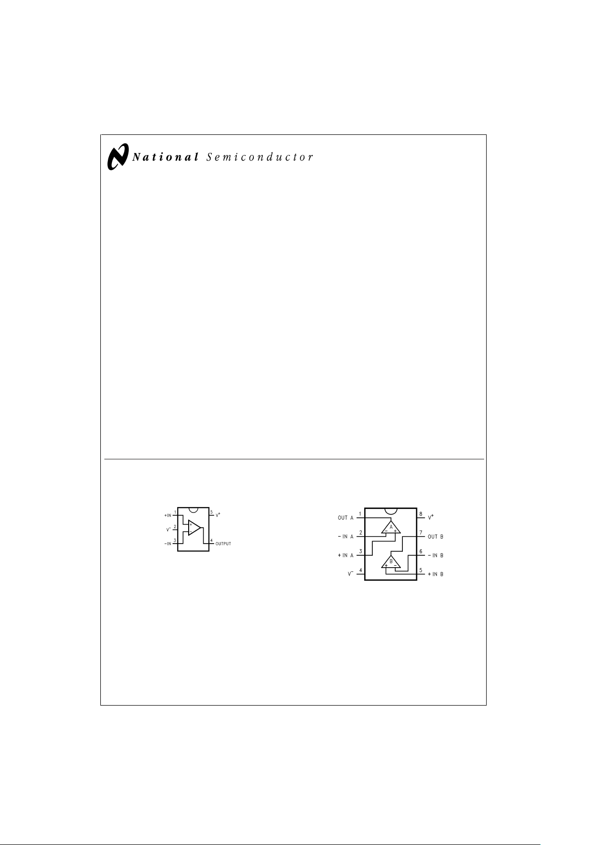
Connection Diagrams
5-Pin SC70-5/SOT23-5
DS100979-84
Top View
8-Pin MSOP/SOIC
DS100979-2
Top View
December 1999
LMV921 Single/ LMV922 Dual/ LMV924 Quad 1.8V, 1MHz, Low Power Operational Amplifiers with
Rail-To-Rail Input and Output
© 1999 National Semiconductor Corporation DS100979 www.national.com
Page 2
Connection Diagrams (Continued)
Ordering Information
Package Temperature Range
Industrial
−40˚C to +85˚C
Packaging
Marking
Transport Media NSC
Drawing
5-Pin SC70-5 LMV921M7 A21 1k Units Tape and Reel MAA05A
LMV921M7X A21 3k Units Tape and Reel
5-Pin SOT23-5 LMV921M5 A29A 1k Units Tape and Reel
MA05B
LMV921M5X A29A 3k Units Tape and Reel
8-Pin MSOP LMV922MM LMV922 1k Units Tape and Reel
MUA08A
LMV922MMX LMV922 3.5k Units Tape and Reel
14-Pin TSSOP LMV924MT LMV924 Rails
MTC14
LMV924MTX LMV924 2.5k Units Tape and Reel
8-Pin SOIC LMV922M LMV922M Rails
M08A
LMV922MX LMV922M 2.5k Units Tape and Reel
14-Pin SOIC LMV924M LMV924M Rails
M14A
LMV924MX LMV924M 2.5k Units Tape and Reel
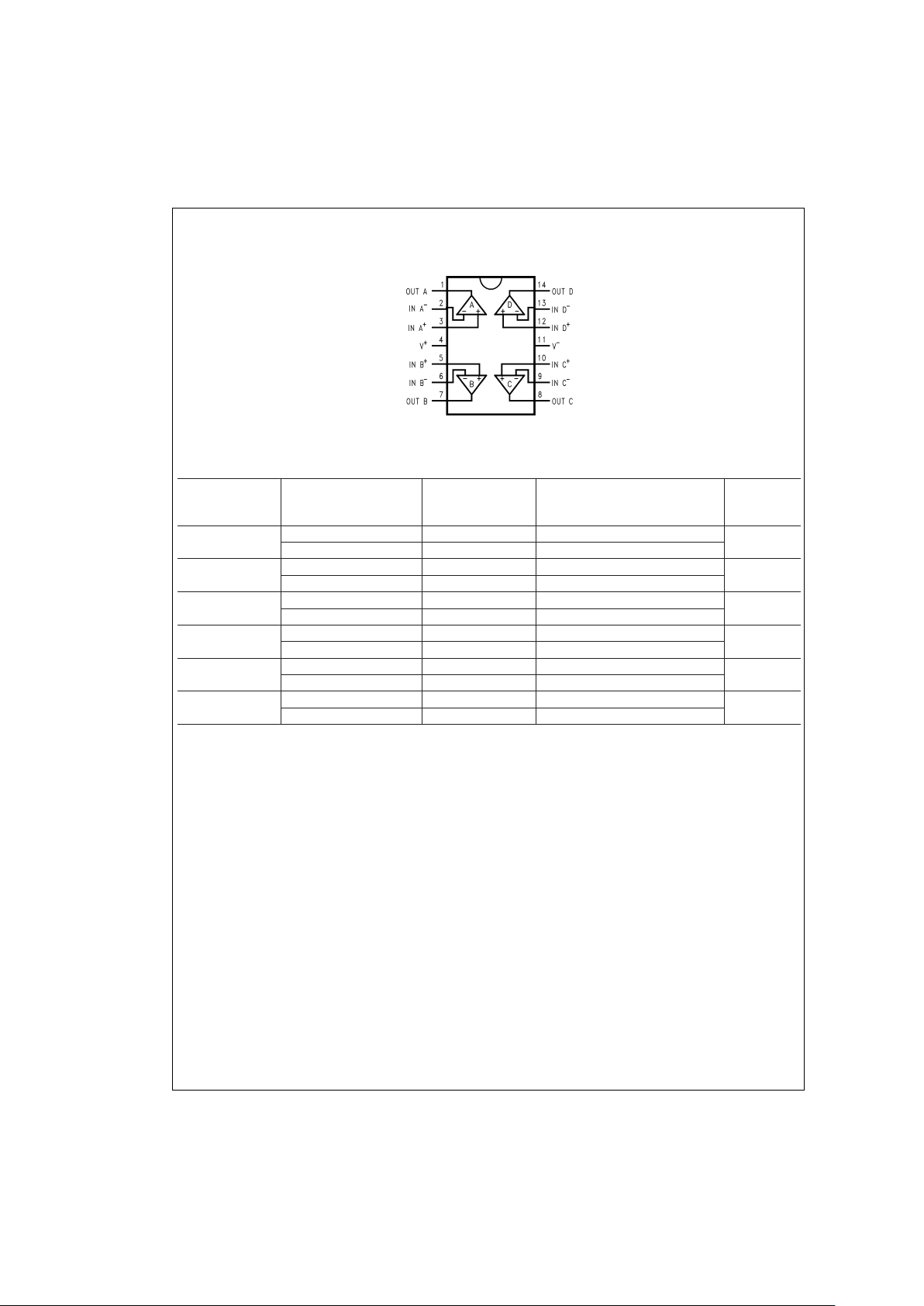
14-Pin TSSOP/SOIC
DS100979-1
Top View
LMV921 Single/ LMV922 Dual/ LMV924 Quad
www.national.com 2
Page 3
Absolute Maximum Ratings (Note 1)
If Military/Aerospace specified devices are required,
please contact the National Semiconductor Sales Office/
Distributors for availability and specifications.
ESD Tolerance (Note 2)
Machine Model 100V
Human Body Model 2000V
Differential Input Voltage
±
Supply Voltage
Supply Voltage (V
+–V−
) 5.5V
Output Short Circuit to V
+
(Note 3)
Output Short Circuit to V
−
(Note 3)
Storage Temperature Range −65˚C to 150˚C
Junction Temperature (Note 4) 150˚C
Mounting Temp.
Infrared or Convection (20 sec) 235˚C
Operating Ratings (Note 1)
Supply Voltage 1.5V to 5.0V
Temperature Range −40˚C ≤ T
J
≤ 85˚C
Thermal Resistance (θ
JA
)
Ultra Tiny SC70-5 Package
5-Pin Surface Mount 440 ˚C/W
Tiny SOT23-5 Package
5-Pin Surface Mount 265 ˚C/W
MSOP Package
8-Pin Surface Mount 235˚C/W
TSSOP Package
14-Pin Surface Mount 155˚C/W
SOIC Package
8-Pin Surface Mount 175˚C/W
14-Pin Surface Mount 127˚C/W
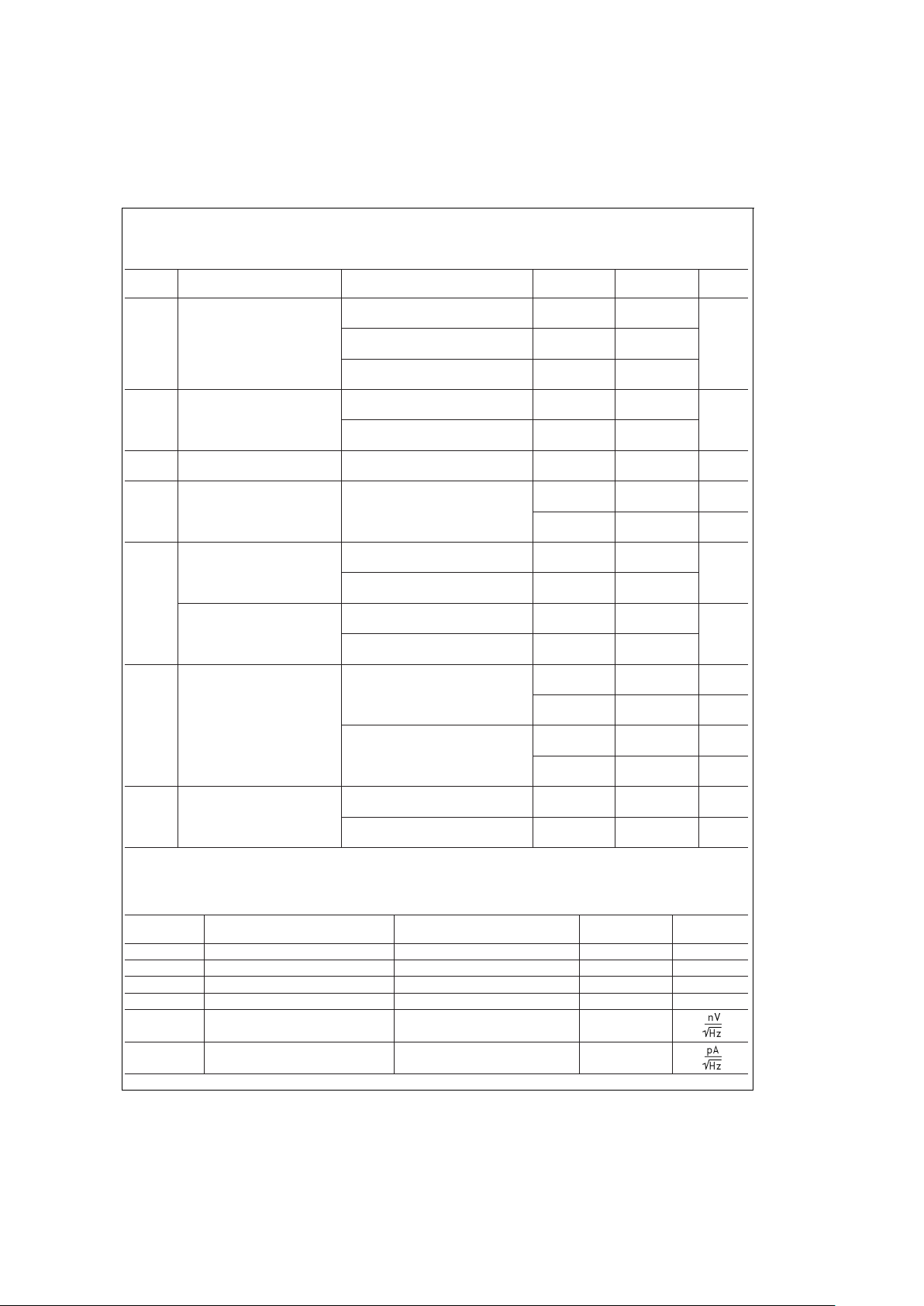
1.8V DC Electrical Characteristics
Unless otherwise specified, all limits guaranteed for TJ= 25˚C. V+= 1.8V, V−= 0V, VCM=V+/2, VO=V+/2 and
R
L
>
1MΩ.Boldface limits apply at the temperature extremes.
Symbol Parameter Condition Typ
(Note 5)
Limits
(Note 6)
Units
V
OS
Input Offset Voltage LMV921 (Single) −1.8 6
8
mV
max
LMV922 (Dual)
LMV924 (Quad)
−1.8 8
9.5
mV
max
TCV
OS
Input Offset Voltage Average
Drift
1 µV/˚C
I
B
Input Bias Current 12 35
50
nA
max
I
OS
Input Offset Current 2 25
40
nA
max
I
S
Supply Current LMV921 (Single) 145 185
205
µA
max
LMV922 (Dual) 330 400
550
LMV924 (Quad) 560 700
850
CMRR Common Mode Rejection Ratio 0 ≤ V
CM
≤ 0.6V 82 62
60
dB
min
−0.2V ≤ V
CM
≤ 0V
1.8V ≤ V
CM
≤ 2.0V
74 50
PSRR Power Supply Rejection Ratio 1.8V ≤ V
+
≤ 5V,
V
CM
= 0.5V
78 67
62
dB
min
V
CM
Input Common-Mode Voltage
Range
For CMRR ≥ 50dB -0.3 -0.2
0
V
max
2.15 2.0
1.8
V
min
A
V
Large Signal Voltage Gain
LMV921 (Single)
RL= 600Ω to 0.9V,
V
O
= 0.2V to 1.6V, VCM= 0.5V
91 77
73
dB
min
R
L
=2kΩto 0.9V,
V
O
= 0.2V to 1.6V, VCM= 0.5V
95 80
75
Large Signal Voltage Gain
LMV922 (Dual)
LMV924 (Quad)
R
L
= 600Ω to 0.9V,
V
O
= 0.2V to 1.6V, VCM= 0.5V
79 65
61
dB
min
R
L
=2kΩto 0.9V,
V
O
= 0.2V to 1.6V, VCM= 0.5V
83 68
63
LMV921 Single/ LMV922 Dual/ LMV924 Quad
www.national.com3
Page 4
1.8V DC Electrical Characteristics (Continued)
Unless otherwise specified, all limits guaranteed for TJ= 25˚C. V+= 1.8V, V−= 0V, VCM=V+/2, VO=V+/2 and
R
L
>
1MΩ.Boldface limits apply at the temperature extremes.
Symbol Parameter Condition Typ
(Note 5)
Limits
(Note 6)
Units
V
O
Output Swing RL= 600Ω to 0.9V
V
IN
=±100mV
1.7 1.65
1.63
V
min
0.075 0.090
0.105
V
max
R
L
=2kΩto 0.9V
V
IN
=±100mV
1.77 1.75
1.74
V
min
0.025 0.035
0.040
V
max
I
O
Output Short Circuit Current Sourcing, VO=0V
V
IN
= 100mV
64
3.3
mA
min
Sinking, V
O
= 1.8V
V
IN
= −100mV
10 7
5
mA
min
1.8V AC Electrical Characteristics
Unless otherwise specified, all limits guaranteed for TJ= 25˚C. V+= 1.8V, V−= 0V, VCM=V+/2, VO=V+/2 and
R
L
>
1MΩ.Boldface limits apply at the temperature extremes.
Symbol Parameter Conditions Typ
(Note 5)
Units
SR Slew Rate (Note 7) 0.39 V/µs
GBW Gain-Bandwidth Product 1 MHz
Φ
m
Phase Margin 60 Deg.
G
m
Gain Margin 10 dB
e
n
Input-Referred Voltage Noise f = 1 kHz, VCM= 0.5V 45
i
n
Input-Referred Current Noise f = 1 kHz 0.1
THD Total Harmonic Distortion f=1kHz, A
V
=
+1
R
L
=
600kΩ,V
IN
=
1V
PP
0.089
%
Amp-to-Amp Isolation (Note 8) 140 dB
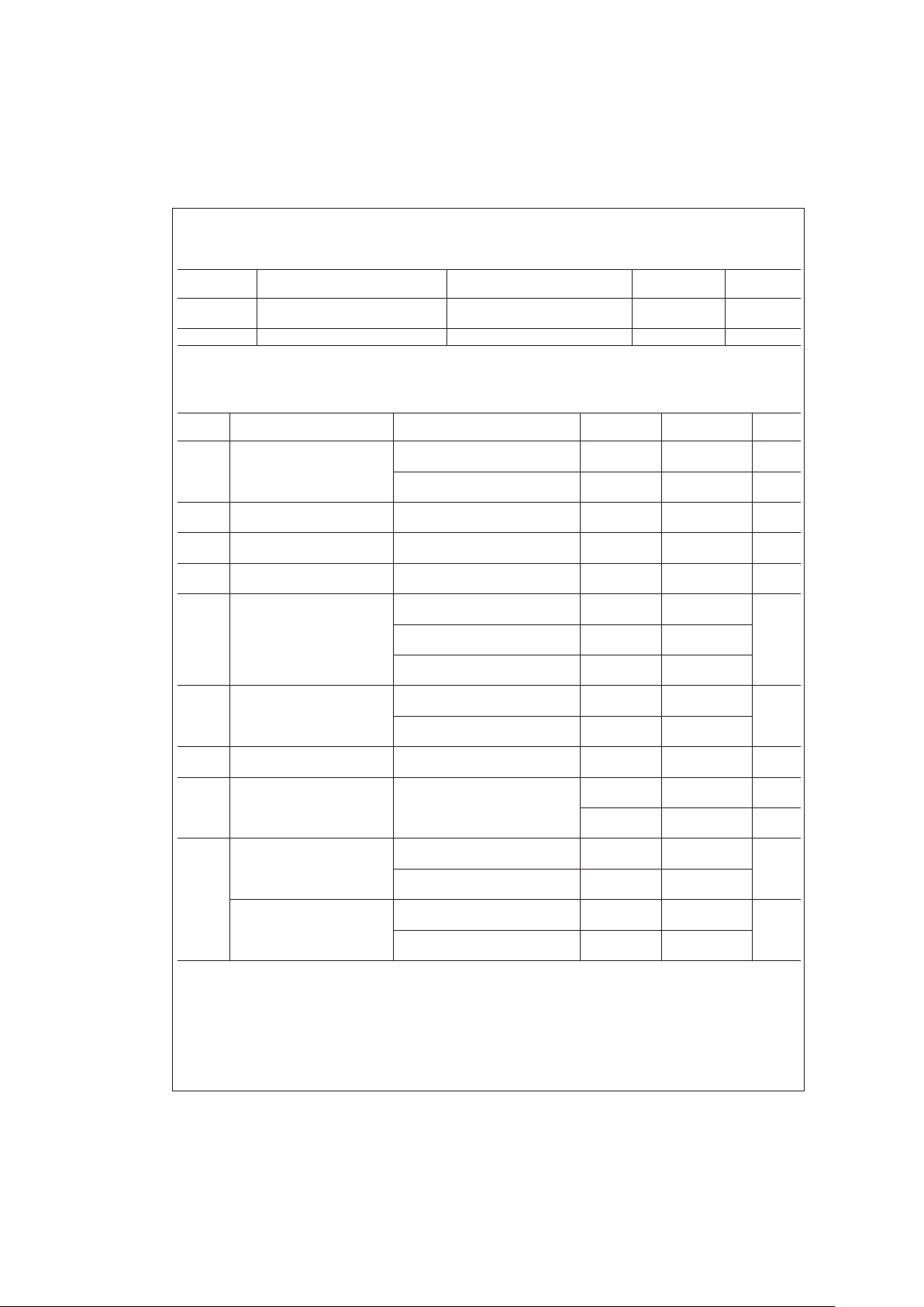
2.7V DC Electrical Characteristics
Unless otherwise specified, all limits guaranteed for TJ= 25˚C. V+= 2.7V, V−= 0V, VCM=V+/2, VO=V+/2 and
R
L
>
1MΩ.Boldface limits apply at the temperature extremes.
Symbol Parameter Condition Typ
(Note 5)
Limits
(Note 6)
Units
V
OS
Input Offset Voltage LMV921 (Single) −1.6 6
8
mV
max
LMV922 (Dual)
LMV924 (Quad)
−1.6 8
9.5
mV
max
TCV
OS
Input Offset Voltage Average
Drift
1 µV/˚C
I
B
Input Bias Current 12 35
50
nA
max
I
OS
Input Offset Current 2 25
40
nA
max
LMV921 Single/ LMV922 Dual/ LMV924 Quad
www.national.com 4
Page 5
2.7V DC Electrical Characteristics (Continued)
Unless otherwise specified, all limits guaranteed for TJ= 25˚C. V+= 2.7V, V−= 0V, VCM=V+/2, VO=V+/2 and
R
L
>
1MΩ.Boldface limits apply at the temperature extremes.
Symbol Parameter Condition Typ
(Note 5)
Limits
(Note 6)
Units
I
S
Supply Current LMV921 (Single) 147 190
210
uA
max
LMV922 (Dual) 380 450
600
LMV924 (Quad) 580 750
900
CMRR Common Mode Rejection Ratio 0V ≤ V
CM
≤ 1.5V 84 62
60
dB
min
−0.2V ≤ V
CM
≤ 0V
2.7V ≤ V
CM
<
2.9V
73 50
PSRR Power Supply Rejection Ratio 1.8V ≤ V
+
≤ 5V,
V
CM
= 0.5V
78 67
62
dB
min
V
CM
Input Common-Mode Voltage
Range
For CMRR ≥ 50dB -0.3 -0.2
0
V
max
3.050 2.9
2.7
V
min
A
V
Large Signal Voltage Gain
LMV921 (Single)
RL= 600Ω to 1.35V,
V
O
= 0.2V to 2.5V
98 80
75
dB
min
R
L
=2kΩto 1.35V,
V
O
= 0.2V to 2.5V
103 83
77
Large Signal Voltage Gain
LMV922 (Dual)
LMV924 (Quad)
R
L
= 600Ω to 1.35V,
V
O
= 0.2V to 2.5V
86 68
63
dB
min
R
L
=2kΩto 1.35V,
V
O
= 0.2V to 2.5V
91 71
65
V
O
Output Swing RL= 600Ω to 1.35V
V
IN
=±100mV
2.62 2.550
2.530
V
min
0.075 0.095
0.115
V
max
R
L
=2kΩto 1.35V
V
IN
=±100mV
2.675 2.650
2.640
V
min
0.025 0.040
0.045
V
max
I
O
Output Short Circuit Current Sourcing, VO=0V
V
IN
= 100mV
27 20
15
mA
min
Sinking, V
O
= 2.7V
V
IN
= −100mV
28 22
16
mA
min
2.7V AC Electrical Characteristics
Unless otherwise specified, all limits guaranteed for TJ= 25˚C. V+= 2.7V, V−= 0V, VCM= 1.0V, VO= 1.35V and
R
L
>
1MΩ.Boldface limits apply at the temperature extremes.
Symbol Parameter Conditions Typ
(Note 5)
Units
SR Slew Rate (Note 7) 0.41 V/µs
GBW Gain-Bandwidth Product 1 MHz
Φ
m
Phase Margin 65 Deg.
G
m
Gain Margin 10 dB
e
n
Input-Referred Voltage Noise f = 1 kHz, VCM= 0.5V 45
i
n
Input-Referred Current Noise f = 1 kHz 0.1
LMV921 Single/ LMV922 Dual/ LMV924 Quad
www.national.com5
Page 6
2.7V AC Electrical Characteristics (Continued)
Unless otherwise specified, all limits guaranteed for TJ= 25˚C. V+= 2.7V, V−= 0V, VCM= 1.0V, VO= 1.35V and
R
L
>
1MΩ.Boldface limits apply at the temperature extremes.
Symbol Parameter Conditions Typ
(Note 5)
Units
THD Total Harmonic Distortion f=1 kHz, A
V
=
+1
R
L
=
600kΩ,V
IN
=
1V
PP
0.077
%
Amp-to-Amp Isolation (Note 8) 140 dB
5V DC Electrical Characteristics
Unless otherwise specified, all limits guaranteed for TJ= 25˚C. V+= 5V, V−= 0V, VCM=V+/2, VO=V+/2 and
R
L
>
1MΩ.Boldface limits apply at the temperature extremes.
Symbol Parameter Condition Typ
(Note 5)
Limits
(Note 6)
Units
V
OS
Input Offset Voltage LMV921 (Single) −1.5 6
8
mV
max
LMV922 (Dual)
LMV924 (Quad)
−1.5 8
9.5
mV
max
TCV
OS
Input Offset Voltage Average
Drift
1 µV/˚C
I
B
Input Bias Current 12 35
50
nA
max
I
OS
Input Offset Current 2 25
40
nA
max
I
S
Supply Current LMV921 (Single) 160 210
230
µA
max
LMV922 (Dual) 400 500
700
LMV924 (Quad) 750 850
980
CMRR Common Mode Rejection Ratio 0V ≤ V
CM
≤ 3.8V 86 62
61
dB
min
−0.2V ≤ V
CM
≤ 0V
5.0V ≤ V
CM
≤ 5.2V
72 50
PSRR Power Supply Rejection Ratio 1.8V ≤ V
+
≤ 5V
V
CM
= 0.5V
78 67
62
dB
min
V
CM
Input Common-Mode Voltage
Range
For CMRR ≥ 50dB -0.3 -0.2
0
V
max
5.350 5.2
5.0
V
min
A
V
Voltage Gain
LMV921 (Single)
RL= 600Ω to 2.5V
V
O
= 0.2V to 4.8V
104 86
82
dB
min
R
L
=2kΩto 2.5V
V
O
= 0.2V to 4.8V
108 89
85
Voltage Gain
LMV922 (Dual)
LMV924 (Quad)
R
L
= 600Ω to 2.5V
V
O
= 0.2V to 4.8V
90 72
68
dB
min
R
L
=2kΩto 2.5V
V
O
= 0.2V to 4.8V
96 77
73
LMV921 Single/ LMV922 Dual/ LMV924 Quad
www.national.com 6
Page 7
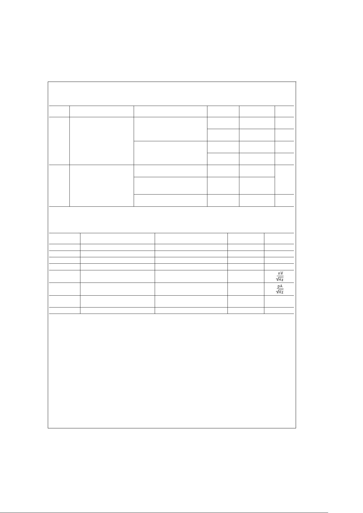
5V DC Electrical Characteristics (Continued)
Unless otherwise specified, all limits guaranteed for TJ= 25˚C. V+= 5V, V−= 0V, VCM=V+/2, VO=V+/2 and
R
L
>
1MΩ.Boldface limits apply at the temperature extremes.
Symbol Parameter Condition Typ
(Note 5)
Limits
(Note 6)
Units
V
O
Output Swing RL= 600Ω to 2.5V
V
IN
=±100mV
4.895 4.865
4.840
V
min
0.1 0.135
0.160
V
max
R
L
=2kΩto 2.5V
V
IN
=±100mV
4.965 4.945
4.935
V
min
0.035 0.065
0.075
V
max
I
O
Output Short Circuit Current LMV921 Sourcing, VO=0V
V
IN
= 100mV
98 85
68
mA
min
LMV922, LMV924 Sourcing, V
O
=
0V
V
IN
= 100mV
60 35
Sinking, V
O
=5V
V
IN
= −100mV
75 65
45
mA
min
5V AC Electrical Characteristics
Unless otherwise specified, all limits guaranteed for TJ= 25˚C. V+= 5V, V−= 0V, VCM=V+/2, VO= 2.5V and
R
L
>
1MΩ.Boldface limits apply at the temperature extremes.
Symbol Parameter Conditions Typ
(Note 5)
Units
SR Slew Rate (Note 7) 0.45 V/µs
GBW Gain-Bandwidth Product 1 MHz
Φ
m
Phase Margin 70 Deg.
G
m
Gain Margin 15 dB
e
n
Input-Referred Voltage Noise f = 1 kHz, VCM=1V 45
i
n
Input-Referred Current Noise f = 1 kHz 0.1
THD Total Harmonic Distortion f = 1 kHz, AV=+1
R
L
= 600Ω,VO=1V
PP
0.069
%
Amp-to-Amp Isolation (Note 8) 140 dB
Note 1: Absolute Maximum Ratings indicate limits beyond which damage to the device may occur. Operating Ratings indicate conditions for which the device is intended to be functional, but specific performance is not guaranteed. For guaranteed specifications and the test conditions, see the Electrical Characteristics.
Note 2: Human body model, 1.5 kΩ in series with 100 pF. Machine model, 200Ω in series with 100 pF.
Note 3: Applies to both single-supply and split-supply operation. Continuous short circuit operation at elevated ambient temperature can result in exceeding the
maximum allowed junction temperature of 150˚C. Output currents in excess of 45 mA over long term may adversely affect reliability.
Note 4: The maximum power dissipation is a function of T
J(max)
, θJA, and TA. The maximum allowable power dissipation at any ambient temperature is
P
D
=(T
J(max)–TA
)/θJA. All numbers apply for packages soldered directly into a PC board.
Note 5: Typical Values represent the most likely parametric norm.
Note 6: All limits are guaranteed by testing or statistical analysis.
Note 7: V
+
= 5V. Connected as voltage follower with 5V step input. Number specified is the slower of the positive and negative slew rates.
Note 8: Input referred, V
+
=
5V and R
L
=
100kΩ connected to 2.5V. Each amp excited in turn with 1kHz to produce V
O
=
3V
PP
.
LMV921 Single/ LMV922 Dual/ LMV924 Quad
www.national.com7
Page 8
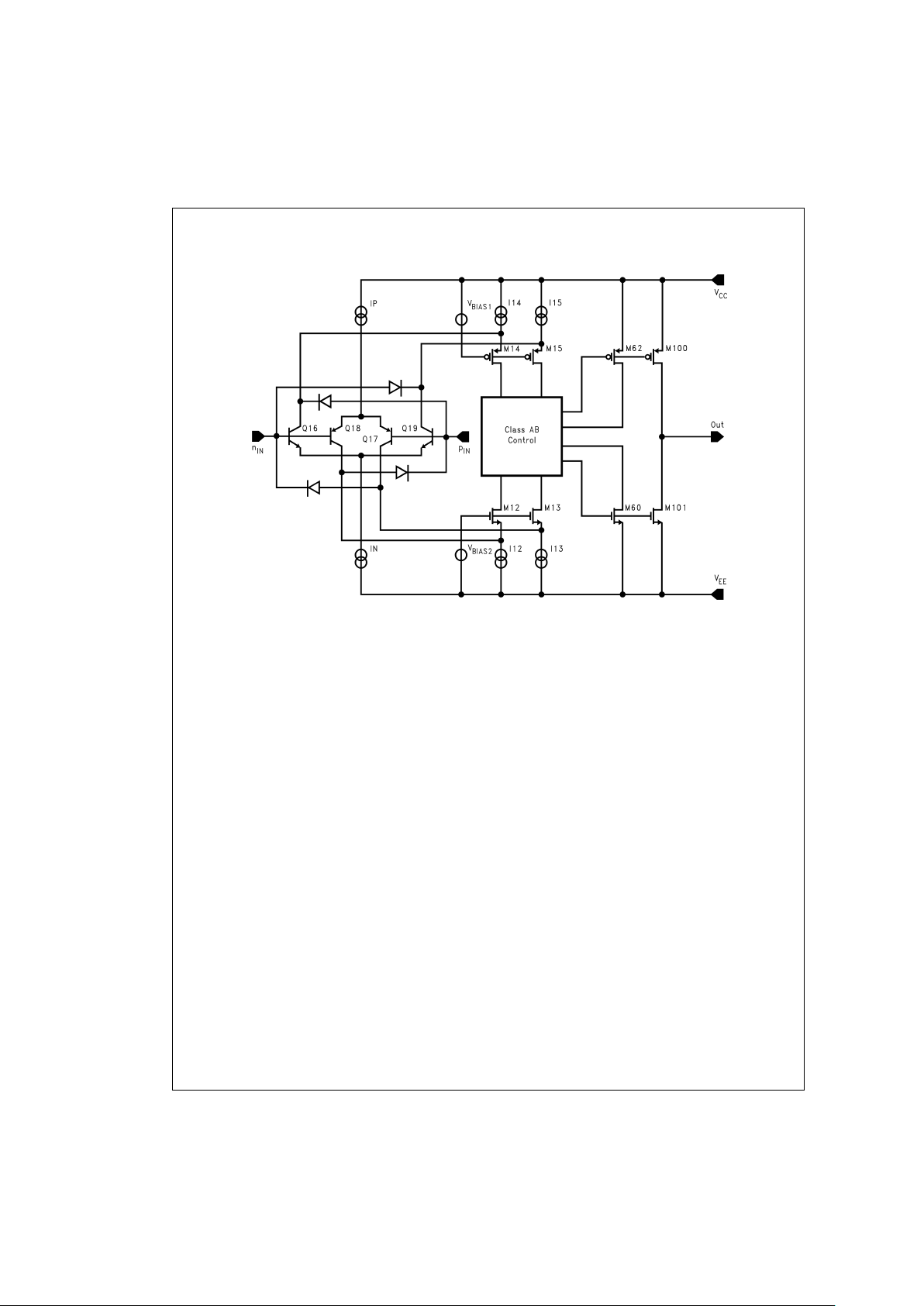
Simplified Schematic
DS100979-A9
LMV921 Single/ LMV922 Dual/ LMV924 Quad
www.national.com 8
Page 9
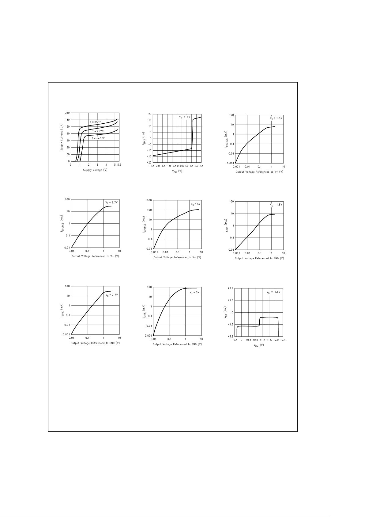
Typical Performance Characteristics Unless otherwise specified, V
S
= +5V, single supply, TA= 25˚C.
Supply Current vs.
Supply Voltage (LMV921)
DS100979-A1
Input Bias Current
vs. V
CM
DS100979-D5
Sourcing Current vs.
Output Voltage
DS100979-B3
Sourcing Current vs.
Output Voltage
DS100979-B8
Sourcing Current vs.
Output Voltage
DS100979-B2
Sinking Current vs.
Output Voltage
DS100979-B4
Sinking Current vs.
Output Voltage
DS100979-B7
Sinking Current vs.
Output Voltage
DS100979-B1
Offset Voltage vs.
Common Mode Voltage
DS100979-D1
LMV921 Single/ LMV922 Dual/ LMV924 Quad
www.national.com9
Page 10

Typical Performance Characteristics Unless otherwise specified, V
S
= +5V, single supply,
T
A
= 25˚C. (Continued)
Offset Voltage vs.
Common Mode Voltage
DS100979-C9
Offset Voltage vs.
Common Mode Voltage
DS100979-C8
Output Voltage Swing vs.
Supply Voltage
DS100979-A2
Output Voltage Swing vs.
Supply Voltage
DS100979-A3
Gain and Phase Margin
vs. Frequency
DS100979-A6
Gain and Phase Margin
vs. Frequency
DS100979-A5
Gain and Phase Margin
vs. Frequency
DS100979-A4
Gain and Phase Margin
vs. Frequency
DS100979-A8
Gain and Phase Margin
vs. Frequency
DS100979-A7
LMV921 Single/ LMV922 Dual/ LMV924 Quad
www.national.com 10
Page 11

Typical Performance Characteristics Unless otherwise specified, V
S
= +5V, single supply,
T
A
= 25˚C. (Continued)
CMRR vs.
Frequency
DS100979-C7
PSRR vs.
Frequency
DS100979-C6
Input Voltage Noise vs.
Frequency
DS100979-F4
Input Current Noise vs.
Frequency
DS100979-F5
THD vs.
Frequency
DS100979-D4
THD vs.
Frequency
DS100979-D3
Slew Rate vs.
Supply Voltage
DS100979-99
Small Signal
Non-Inverting Response
DS100979-E3
Small Signal
Non-Inverting Response
DS100979-E2
LMV921 Single/ LMV922 Dual/ LMV924 Quad
www.national.com11
Page 12

Typical Performance Characteristics Unless otherwise specified, V
S
= +5V, single supply,
T
A
= 25˚C. (Continued)
Small Signal
Non-Inverting Response
DS100979-E4
Small Signal
Inverting Response
DS100979-E0
Small Signal
Inverting Response
DS100979-D9
Small Signal
Inverting Response
DS100979-D8
Small Signal
Non-Inverting Response
DS100979-E6
Small Signal
Non-Inverting Response
DS100979-E7
Small Signal
Non-Inverting Response
DS100979-E5
Small Signal
Inverting Response
DS100979-G3
Small Signal
Inverting Response
DS100979-G2
LMV921 Single/ LMV922 Dual/ LMV924 Quad
www.national.com 12
Page 13

Typical Performance Characteristics Unless otherwise specified, V
S
= +5V, single supply,
T
A
= 25˚C. (Continued)
*
For large signal pulse response in the unity gain follower configuration, the input is 5mV below the positive rail and 5mV above
the negative rail at 25˚C and 85˚C. At −40˚C, input is 10mV below the positive rail and 10mV above the negative rail.
Small Signal
Inverting Response
DS100979-G1
*
Large Signal
Non-Inverting Response
DS100979-F0
*
Large Signal
Non-Inverting Response
DS100979-E9
*
Large Signal
Non-Inverting Response
DS100979-G0
*
Large Signal
Inverting Response
DS100979-F9
*
Large Signal
Inverting Response
DS100979-F8
*
Large Signal
Inverting Response
DS100979-F7
*
Large Signal
Non-Inverting Response
DS100979-F1
*
Large Signal
Non-Inverting Response
DS100979-F2
LMV921 Single/ LMV922 Dual/ LMV924 Quad
www.national.com13
Page 14

Typical Performance Characteristics Unless otherwise specified, V
S
= +5V, single supply,
T
A
= 25˚C. (Continued)
*
For large signal pulse response in the unity gain follower configuration, the input is 5mV below the positive rail and 5mV above
the negative rail at 25˚C and 85˚C. At −40˚C, input is 10mV below the positive rail and 10mV above the negative rail.
*
Large Signal
Inverting Response
DS100979-F6
*
Large Signal
Inverting Response
DS100979-D6
*
Large Signal
Inverting Response
DS100979-E1
*
Large Signal
Inverting Response
DS100979-D7
Short Circuit Current vs.
Temperature (sinking)
DS100979-B5
Short Circuit Current vs.
Temperature (sourcing)
DS100979-B6
LMV921 Single/ LMV922 Dual/ LMV924 Quad
www.national.com 14
Page 15

Application Note
1.0 Unity Gain Pulse Response Considerations
The unity-gain follower is the most sensitive configuration to
capacitive loading. The LMV921/LMV922/LMV924 family
can directly drive 1nF in a unity-gain with minimal ringing. Direct capacitive loading reduces the phase margin of the amplifier. The combination of the amplifier’s output impedance
and the capacitive load induces phase lag. This results in either an underdamped pulse response or oscillation. The
pulse response can be improved by adding a pull up resistor
as shown in
Figure 1
Higher capacitances can be driven by decreasing the value
of the pull-up resistor, but its value shouldn’t be reduced beyond the sinking capability of the part. An alternate approach
is to use an isolation resistor as illustrated in
Figure 2
.
2.0 Input Bias Current Consideration
The LMV921/LMV922/LMV924 family has a bipolar input
stage. The typical input bias current (I
B
) is 12nA. The input
bias current can develop a significant offset voltage. This offset is primarily due to I
B
flowing through the negative feed-
back resistor, R
F
. For example, if IBis 50nA (max room) and
R
F
is 100kΩ, then an offset voltage of 5mV will develop (V
OS
=
I
BXRF
). Using a compensation resistor (RC), as shown in
Figure 3
, cancels this affect. But the input offset current (IOS)
will still contribute to an offset voltage in the same manner.
3.0 Operating Supply Voltage
The LMV921/LMV922/LMV924 family is guaranteed to operate from 1.8V to 5.0V. They will begin to function at power
voltages as low as 1.2V at room temperature when unloaded. Start up voltage increases to 1.5V when the amplifier
is fully loaded (600Ω to mid-supply). Below 1.2V the output
voltage is not guaranteed to follow the input.
Figure 4
below
shows the output voltage vs. supply voltage with the
LMV921/LMV922/LMV924 configured as a voltage follower
at room temperature.
4.0 Input and Output Stage
The rail-to-rail input stage of this family provides more flexibility for the designer. The LMV921/LMV922/LMV924 use a
complimentary PNP and NPN input stage in which the PNP
stage senses common mode voltage near V
−
and the NPN
stage senses common mode voltage near V
+
. The transition
from the PNP stage to NPN stage occurs 1V below V
+
. Since
both input stages have their own offset voltage, the offset of
the amplifier becomes a function of the input common mode
voltage and has a crossover point at 1V below V
+
as shown
in the V
OS
vs. VCMcurves.
DS100979-41
FIGURE 1. Using a Pull-Up Resistor at the Output for
Stabilizing Capacitive Loads
DS100979-43
FIGURE 2. Using an Isolation Resistor to Drive Heavy
Capacitive Loads
DS100979-59
FIGURE 3. Canceling the Voltage Offset Effect of Input
Bias Current
DS100979-D2
FIGURE 4.
LMV921 Single/ LMV922 Dual/ LMV924 Quad
www.national.com15
Page 16

Application Note (Continued)
This V
OS
crossover point can create problems for both DC
and AC coupled signals if proper care is not taken. For large
input signals that include the V
OS
crossover point in their dynamic range, this will cause distortion in the output signal.
One way to avoid such distortion is to keep the signal away
from the crossover. For example, in a unity gain buffer configuration and with V
S
=
5V, a 5V peak-to-peak signal will
contain input-crossover distortion while a 3V peak-to-peak
signal centered at 1.5V will not contain input-crossover distortion as it avoids the crossover point. Another way to avoid
large signal distortion is to use a gain of −1 circuit which
avoids any voltage excursions at the input terminals of the
amplifier. In that circuit, the common mode DC voltage can
be set at a level away from the V
OS
cross-over point.
For small signals, this transition in V
OS
shows up as a V
CM
dependent spurious signal in series with the input signal and
can effectively degrade small signal parameters such as
gain and common mode rejection ratio. To resolve this problem, the small signal should be placed such that it avoids the
V
OS
crossover point.
In addition to the rail-to-rail performance, the output stage
can provide enough output current to drive 600Ω loads. Because of the high current capability, care should be taken not
to exceed the 150˚C maximum junction temperature specification.
5.0 Power-Supply Considerations
The LMV921/LMV922/LMV924 are ideally suited for use with
most battery-powered systems. The LMV921/LMV922/
LMV924 operate from a single +1.8V to +5.0V supply and
consumes about 145µA of supply current per Amplifier. A
high power supply rejection ratio of 78dB allows the amplifier
to be powered directly off a decaying battery voltage extending battery life.
Table1
lists a variety of typical battery types. Batteries have
different voltage ratings; operating voltage is the battery voltage under nominal load. End-of-Life voltage is defined as the
voltage at which 100%of the usable power of the battery is
consumed.
Table 1
also shows the typical operating time of
the LMV921.
6.0 Distortion
The two main contributors of distortion in LMV921/LMV922/
LMV924 family is:
1. Output crossover distortion occurs as the output transitions from sourcing current to sinking current.
2. Input crossover distortion occurs as the input switches
from NPN to PNP transistor at the input stage.
To decrease crossover distortion:
1. Increase the load resistance. This lowers the output crossover distortion but has no effect on the input crossover distortion.
2. Operate from a single supply with the output always
sourcing current.
3. Limit the input voltage swing for large signals between
ground and one volt below the positive supply.
4. Operate in inverting configuration to eliminate common
mode induced distortion.
5.Avoid small input signal around the input crossover region.
The discontinuity in the offset voltage will effect the gain,
CMRR and PSRR.
TABLE 1. LMV921 Characteristics with Typical Battery Systems.
Battery Type Operating
Voltage (V)
End-of-Life
Voltage (V)
Capacity AA
Size (mA -
h)
LMV921
Operating
time (Hours)
Alkaline 1.5 0.9 1000 6802
Lithium 2.7 2.0 1000 6802
Ni - Cad 1.2 0.9 375 2551
NMH 1.2 1.0 500 3401
LMV921 Single/ LMV922 Dual/ LMV924 Quad
www.national.com 16
Page 17

Typical Applications
1.0 Half-wave Rectifier with Rail-To-Ground Output
Swing
Since the LMV921 input common mode range includes both
positive and negative supply rails and the output can also
swing to either supply, achieving half-wave rectifier functions
in either direction is an easy task. All that is needed are two
external resistors; there is no need for diodes or matched resistors. The half wave rectifier can have either positive or
negative going outputs, depending on the way the circuit is
arranged.
In
Figure 5
the circuit is referenced to ground, while in
Figure
6
the circuit is biased to the positive supply. These configurations implement the half wave rectifier since the LMV921 can
not respond to one-half of the incoming waveform. It can not
respond to one-half of the incoming because the amplifier
can not swing the output beyond either rail therefore the output disengages during this half cycle. During the other half
cycle, however, the amplifier achieves a half wave that can
have a peak equal to the total supply voltage. R
I
should be
large enough not to load the LMV921.
DS100979-C3
DS100979-C2
DS100979-C4
FIGURE 5. Half-Wave Rectifier with Rail-To-Ground Output Swing Referenced to Ground
DS100979-C0
DS100979-B9
DS100979-C1
FIGURE 6. Half-Wave Rectifier with Negative-Going Output Referenced to V
CC
LMV921 Single/ LMV922 Dual/ LMV924 Quad
www.national.com17
Page 18

Typical Applications (Continued)
2.0 Instrumentation Amplifier with Rail-To-Rail Input and
Output
Using three of the LMV924 Amplifiers, an instrumentation
amplifier with rail-to-rail inputs and outputs can be made.
Some manufacturers use a precision voltage divider array of
5 resistors to divide the common mode voltage to get a
rail-to-rail input range. The problem with this method is that it
also divides the signal, so in order to get unity gain, the amplifier must be run at high loop gains. This raises the noise
and drift by the internal gain factor and lowers the input impedance. Any mismatch in these precision resistors reduces
the CMRR as well. Using the LMV924 eliminates all of these
problems.
In this example, amplifiers A and B act as buffers to the differential stage. These buffers assure that the input imped-
ance is very high and require no precision matched resistors
in the input stage. They also assure that the difference amp
is driven from a voltage source. This is necessary to maintain the CMRR set by the matching R
1-R2
with R3-R4.
The gain is set by the ratio of R
2/R1
and R3should equal R
1
and R4equal R2.
With both rail-to-rail input and output ranges, the input and
output are only limited by the supply voltages. Remember
that even with rail-to-rail outputs, the output can not swing
past the supplies so the combined common mode voltages
plus the signal should not be greater that the supplies or limiting will occur. For additional applications, see National
Semiconductor application notes AN–29, AN–31, AN–71,
and AN–127.
DS100979-G4
FIGURE 7. Rail-to-rail instrumentation amplifier
LMV921 Single/ LMV922 Dual/ LMV924 Quad
www.national.com 18
Page 19

SC70–5 Tape Dimensions
SOT23–5 and SC70–5 Tape Format
Tape Format
Tape Section
#
Cavities Cavity Status Cover Tape Status
Leader 0 (min) Empty Sealed
(Start End) 75 (min) Empty Sealed
Carrier 3000 Filled Sealed
250 Filled Sealed
Trailer 125 (min) Empty Sealed
(Hub End) 0 (min) Empty Sealed
DS100979-96
LMV921 Single/ LMV922 Dual/ LMV924 Quad
www.national.com19
Page 20

SOT23–5 Tape Dimensions
8 mm 0.130 0.124 0.130 0.126 0.138±0.002 0.055±0.004 0.157 0.315±0.012
(3.3) (3.15) (3.3) (3.2) (3.5
±
0.05) (1.4±0.11) (4) (8±0.3)
Tape Size DIM A DIM Ao DIM B DIM Bo DIM F DIM Ko DIM P1 DIM W
DS100979-97
LMV921 Single/ LMV922 Dual/ LMV924 Quad
www.national.com 20
Page 21

SOT23–5 and SC70–5 Reel Dimensions
8 mm 7.00 0.059 0.512 0.795 2.165 0.331 + 0.059/−0.000 0.567 W1+ 0.078/−0.039
330.00 1.50 13.00 20.20 55.00 8.40 + 1.50/−0.00 14.40 W1 + 2.00/−1.00
Tape Size A B C D N W1 W2 W3
DS100979-98
LMV921 Single/ LMV922 Dual/ LMV924 Quad
www.national.com21
Page 22

Physical Dimensions inches (millimeters) unless otherwise noted
SC70-5
Order Number LMV921M7 or LMV921M7X
NS Package Number MAA05A
LMV921 Single/ LMV922 Dual/ LMV924 Quad
www.national.com 22
Page 23

Physical Dimensions inches (millimeters) unless otherwise noted (Continued)
SOT 23-5
Order Number LMV921M5 or LMV921M5X
NS Package Number MA05B
LMV921 Single/ LMV922 Dual/ LMV924 Quad
www.national.com23
Page 24

Physical Dimensions inches (millimeters) unless otherwise noted (Continued)
8-Pin MSOP
Order Number LMV922MM or LMV922MMX
NS Package Number MUA08A
LMV921 Single/ LMV922 Dual/ LMV924 Quad
www.national.com 24
Page 25

Physical Dimensions inches (millimeters) unless otherwise noted (Continued)
14-Pin TSSOP
Order Number LMV924MT or LMV924MTX
NS Package Number MTC14
LMV921 Single/ LMV922 Dual/ LMV924 Quad
www.national.com25
Page 26

Physical Dimensions inches (millimeters) unless otherwise noted (Continued)
8-Pin SOIC
Order Number LMV922M or LMV922MX
NS Package Number M08A
LMV921 Single/ LMV922 Dual/ LMV924 Quad
www.national.com 26
Page 27

Physical Dimensions inches (millimeters) unless otherwise noted (Continued)
LIFE SUPPORT POLICY
NATIONAL’S PRODUCTS ARE NOT AUTHORIZED FOR USE AS CRITICAL COMPONENTS IN LIFE SUPPORT
DEVICES OR SYSTEMS WITHOUT THE EXPRESS WRITTEN APPROVAL OF THE PRESIDENT AND GENERAL
COUNSEL OF NATIONAL SEMICONDUCTOR CORPORATION. As used herein:
1. Life support devices or systems are devices or
systems which, (a) are intended for surgical implant
into the body, or (b) support or sustain life, and
whose failure to perform when properly used in
accordance with instructions for use provided in the
labeling, can be reasonably expected to result in a
significant injury to the user.
2. A critical component is any component of a life
support device or system whose failure to perform
can be reasonably expected to cause the failure of
the life support device or system, or to affect its
safety or effectiveness.
National Semiconductor
Corporation
Americas
Tel: 1-800-272-9959
Fax: 1-800-737-7018
Email: support@nsc.com
National Semiconductor
Europe
Fax: +49 (0) 1 80-530 85 86
Email: europe.support@nsc.com
Deutsch Tel: +49 (0) 1 80-530 85 85
English Tel: +49 (0) 1 80-532 78 32
Français Tel: +49 (0) 1 80-532 93 58
Italiano Tel: +49 (0) 1 80-534 16 80
National Semiconductor
Asia Pacific Customer
Response Group
Tel: 65-2544466
Fax: 65-2504466
Email: sea.support@nsc.com
National Semiconductor
Japan Ltd.
Tel: 81-3-5639-7560
Fax: 81-3-5639-7507
www.national.com
14-Pin SOIC
Order Number LMV924M or LMV924MX
NS Package Number MA14
LMV921 Single/ LMV922 Dual/ LMV924 Quad 1.8V, 1MHz, Low Power Operational Amplifiers with
Rail-To-Rail Input and Output
National does not assume any responsibility for use of any circuitry described, no circuit patent licenses are implied and National reserves the right at any time without notice to change said circuitry and specifications.
 Loading...