

Page 1
March 2007
LMV841 / LMV844
CMOS Input, RRIO, Wide Supply Range Operational
Amplifiers
General Description
The LMV841 and LMV844 are low-voltage and low-power
operational amplifiers that operate with supply voltages ranging from 2.7V to 12V and have rail-to-rail input and output
capability.
The LMV841 and LMV844 are low offset voltage and low
supply current amplifiers with MOS inputs, characteristics that
make the LMV841/LMV844 ideal for sensor interface and
battery powered applications.
The LMV841 is offered in the space saving 5-pin SC70 package and the quad LMV844 comes in the 14-Pin TSSOP
package. These small packages are solutions for area constrained PC boards and portable electronics.
Features
Unless otherwise noted, typical values at TA = 25°C, V+ = 5V
■
Space saving 5-Pin SC70 package
■
Supply voltage range 2.7V to 12V
■
Guaranteed at 3.3V, 5V and ±5V
■
Low supply current 1 mA per channel
■
Unity gain bandwidth 4.5 MHz
■
Open loop gain 100 dB
■
Input offset voltage
500 μV max
■
Input bias current 0.3 pA
■
CMRR 100 dB
■
Input voltage noise 20 nV/
■
Temperature range −40°C to 125°C
■
Rail-to-rail input
■
Rail-to-rail output
Applications
■
High impedance sensor interface
■
Battery powered instrumentation
■
High gain amplifiers
■
DAC buffer
■
Instrumentation amplifiers
■
Active Filters
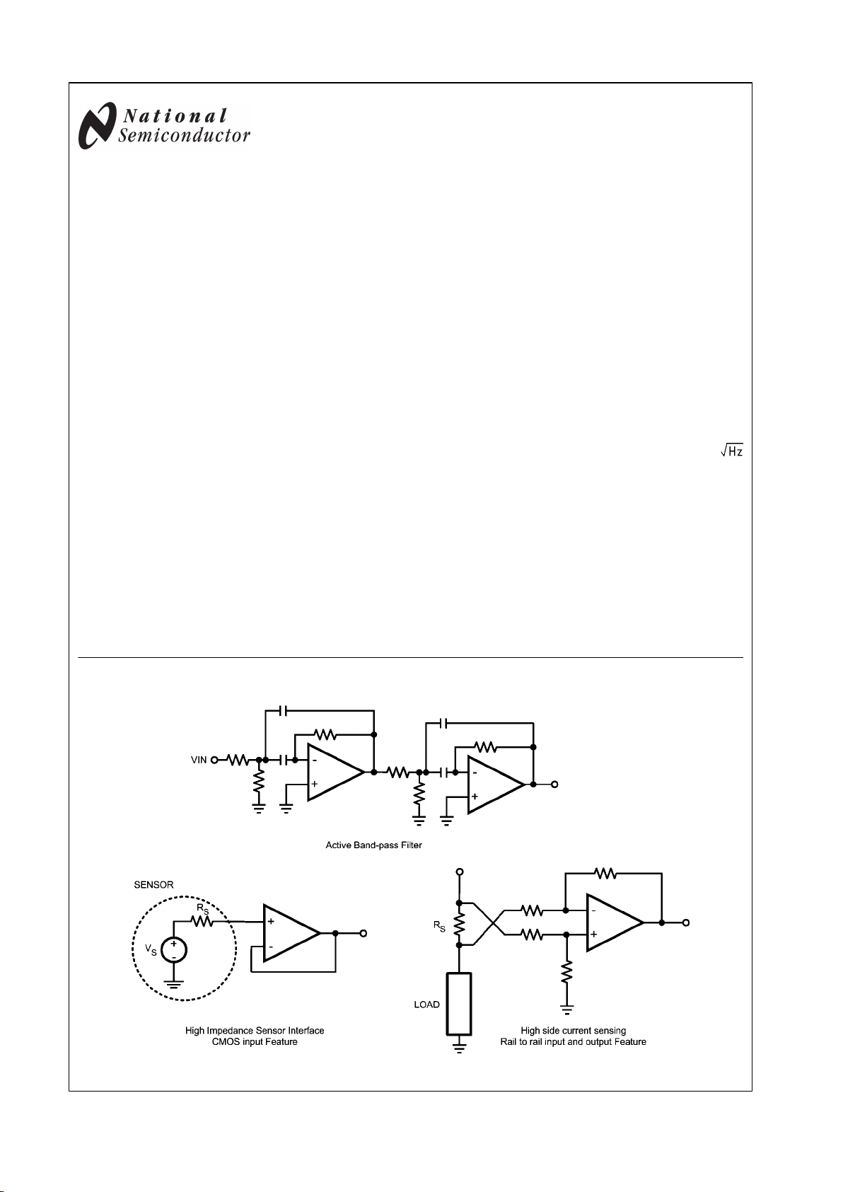
Typical Applications
20168301
© 2007 National Semiconductor Corporation 201683 www.national.com
LMV841 Single / LMV844 Quad CMOS Input, RRIO, Wide Supply Range Operational Amplifiers
Page 2
Absolute Maximum Ratings (Note 1)
If Military/Aerospace specified devices are required,
please contact the National Semiconductor Sales Office/
Distributors for availability and specifications.
ESD Tolerance (Note 2)
Human Body Model 2 kV
Machine Model 200V
V
IN
Differential
±300 mV
Supply Voltage (V+ – V−)
13.2V
Voltage at Input/Output Pins V++0.3V, V− −0.3V
Input Current 10 mA
Storage Temperature Range −65°C to +150°C
Junction Temperature (Note 3) +150°C
Soldering Information
Infrared or Convection (20 sec) 235°C
Wave Soldering Lead Temp. (10 sec) 260°C
Operating Ratings (Note 1)
Temperature Range (Note 3) −40°C to +125°C
Supply Voltage (V+ – V−)
2.7V to 12V
Package Thermal Resistance (θJA (Note 3))
5-Pin SC70 334 °C/W
14-Pin TSSOP 110 °C/W
3.3V Electrical Characteristics (Note 4)
Unless otherwise specified, all limits are guaranteed for at TA = 25°C, V+ = 3.3V, V− = 0V, VCM = V+/2, and RL > 10 MΩ to V+/2.
Boldface limits apply at the temperature extremes.
Symbol Parameter Conditions Min
(Note 6)
Typ
(Note 5)
Max
(Note 6)
Units
V
OS
Input Offset Voltage 8 ±500
±800
μV
TCV
OS
Input Offset Voltage Drift (Note 7) 0.5 ±5
μV/°C
I
B
Input Bias Current
(Notes 7, 8)
0.3 10
300
pA
I
OS
Input Offset Current 40
fA
CMRR Common Mode Rejection Ratio
LMV841
0V ≤ V
CM
≤ 3.3V
84
80
100
dB
Common Mode Rejection Ratio
LMV844
77
75
100
PSRR Power Supply Rejection Ratio
2.7V ≤ V+ ≤ 12V, VO = V+/2
86
82
100
dB
CMVR Input Common-Mode Voltage Range
CMRR ≥ 50 dB
–0.1 3.4
V
A
VOL
Large Signal Voltage Gain
RL = 2 kΩ
VO = 0.3V to 3.0V
100
96
118
dB
RL = 10 kΩ
VO = 0.2V to 3.1V
100
96
129
V
O
Output Swing High,
measured from V
+
RL = 2 kΩ to V+/2
60 80
120
mV
RL = 10 kΩ to V+/2
32 50
70
Output Swing Low,
measured from V
−
RL = 2 kΩ to V+/2
70 100
120
mV
RL = 10 kΩ to V+/2
35 65
75
I
O
Output Short Circuit Current
(Notes 3, 9)
Sourcing VO = V+/2
VIN = 100 mV
20
15
30
mA
Sinking VO = V+/2
VIN = −100 mV
20
15
30
I
S
Supply Current Per Channel 0.98 1.5
2
mA
SR Slew Rate (Note 10) AV = +1, VO = 2.3 V
PP
10% to 90%
2.5
V/μs
GBW Gain Bandwidth Product 4.5 MHz
Φ
m
Phase Margin 67
Deg
www.national.com 2
LMV841 Single / LMV844 Quad
Page 3
Symbol Parameter Conditions Min
(Note 6)
Typ
(Note 5)
Max
(Note 6)
Units
e
n
Input-Referred Voltage Noise f = 1 kHz 20
nV/
R
OUT
Open Loop Output Impedance f = 3 MHz 70
Ω
THD+N Total Harmonic Distortion + Noise f = 1 kHz , AV = 1
RL = 10 kΩ
0.005
%
C
IN
Input Capacitance 13
pF
5V Electrical Characteristics (Note 4)
Unless otherwise specified, all limits are guaranteed for at TA = 25°C, V+ = 5V, V− = 0V, VCM = V+/2, and RL > 10 MΩ to V+/2.
Boldface limits apply at the temperature extremes.
Symbol Parameter Conditions Min
(Note 6)
Typ
(Note 5)
Max
(Note 6)
Units
V
OS
Input Offset Voltage −5 ±500
±800
μV
TCV
OS
Input Offset Voltage Drift (Note 7) 0.35 ±5
μV/°C
I
B
Input Bias Current
(Notes 7, 8)
0.3 10
300
pA
I
OS
Input Offset Current 40
fA
CMRR Common Mode Rejection Ratio
LMV841
0V ≤ V
CM
≤ 5V
86
80
100
dB
Common Mode Rejection Ratio
LMV844
81
79
100
PSRR Power Supply Rejection Ratio
2.7V ≤ V+ ≤ 12V, VO = V+/2
86
82
100
dB
CMVR Input Common-Mode Voltage Range
CMRR ≥ 50 dB
−0.2 5.2
V
A
VOL
Large Signal Voltage Gain
RL = 2 kΩ
VO = 0.3V to 4.7V
100
96
118
dB
RL = 10 kΩ
VO = 0.2V to 4.8V
100
96
129
V
O
Output Swing High,
measured from V
+
RL = 2 kΩ to V+/2
70 100
120
mV
RL = 10 kΩ to V+/2
40 50
70
Output Swing Low,
measured from V
-
RL = 2 kΩ to V+/2
82 120
140
mV
RL = 10 kΩ to V+/2
41 70
80
I
O
Output Short Circuit Current
(Notes 3, 9)
Sourcing VO = V+/2
VIN = 100 mV
20
15
30
mA
Sinking VO = V+/2
VIN = −100 mV
20
15
30
I
S
Supply Current Per Channel 1.02 1.5
2
mA
SR Slew Rate (Note 10) AV = +1, VO = 4 V
PP
10% to 90%
2.5
V/μs
GBW Gain Bandwidth Product 4.5 MHz
Φ
m
Phase Margin 67
Deg
e
n
Input-Referred Voltage Noise f = 1 kHz 20
nV/
R
OUT
Open Loop Output Impedance f = 3 MHz 70
Ω
3 www.national.com
LMV841 Single / LMV844 Quad
Page 4
Symbol Parameter Conditions Min
(Note 6)
Typ
(Note 5)
Max
(Note 6)
Units
THD+N Total Harmonic Distortion + Noise f = 1 kHz , AV = 1
RL = 10 kΩ
0.003
%
C
IN
Input Capacitance 13
pF
±5V Electrical Characteristics (Note 4)
Unless otherwise specified, all limits are guaranteed for at TA = 25°C, V+ = 5V, V− = –5V, VCM = 0V, and RL > 10 MΩ to VCM.
Boldface limits apply at the temperature extremes.
Symbol Parameter Conditions Min
(Note 6)
Typ
(Note 5)
Max
(Note 6)
Units
V
OS
Input Offset Voltage −17 ±500
±800
μV
TCV
OS
Input Offset Voltage Drift (Note 7) 0.25 ±5
μV/°C
I
B
Input Bias Current
(Notes 7, 8)
0.3 10
300
pA
I
OS
Input Offset Current 40
fA
CMRR Common Mode Rejection Ratio
LMV841
–5V ≤ V
CM
≤ 5V
86
80
100
dB
Common Mode Rejection Ratio
LMV844
86
80
100
PSRR Power Supply Rejection Ratio
2.7V ≤ V+ ≤ 12V, VO = 0V
86
82
100
dB
CMVR Input Common-Mode Voltage Range
CMRR ≥ 50 dB
−5.2 5.2
V
A
VOL
Large Signal Voltage Gain
RL = 2 kΩ
VO = −4.7V to 4.7V
100
96
118
dB
RL = 10 kΩ
VO = −4.8V to 4.8V
100
96
129
V
O
Output Swing High,
measured from V
+
RL = 2 kΩ to 0V
105 130
155
mV
RL = 10 kΩ to 0V
50 75
95
Output Swing Low,
measured from V
−
RL = 2 kΩ to 0V
115 160
200
mV
RL = 10 kΩ to 0V
53 80
100
I
O
Output Short Circuit Current
(Notes 3, 9)
Sourcing VO = 0V
VIN = 100 mV
20
15
30
mA
Sinking VO = 0V
VIN = −100 mV
20
15
30
I
S
Supply Current Per Channel 1.11 1.7
2
mA
SR Slew Rate (Note 10) AV = +1, VO = 9 V
PP
10% to 90%
2.5
V/μs
GBW Gain Bandwidth Product 4.5 MHz
Φ
m
Phase Margin 67
Deg
e
n
Input-Referred Voltage Noise f = 1 kHz 20
nV/
R
OUT
Open Loop Output Impedance f = 3 MHz 70
Ω
THD+N Total Harmonic Distortion + Noise f = 1 kHz , AV = 1
RL = 10 kΩ
0.006
%
C
IN
Input Capacitance 13
pF
www.national.com 4
LMV841 Single / LMV844 Quad
Page 5
Note 1: Absolute Maximum Ratings indicate limits beyond which damage to the device may occur. Operating Ratings indicate conditions for which the device is
intended to be functional, but specific performance is not guaranteed. For guaranteed specifications and the test conditions, see the Electrical Characteristics
Tables.
Note 2: Human Body Model, applicable std. MIL-STD-883, Method 3015.7. Machine Model, applicable std. JESD22-A115-A (ESD MM std. of JEDEC) FieldInduced Charge-Device Model, applicable std. JESD22-C101-C (ESD FICDM std. of JEDEC).
Note 3: The maximum power dissipation is a function of T
J(MAX)
, θJA, and TA. The maximum allowable power dissipation at any ambient temperature is
PD = (T
J(MAX)
- TA)/ θJA . All numbers apply for packages soldered directly onto a PC board.
Note 4: Electrical table values apply only for factory testing conditions at the temperature indicated. Factory testing conditions result in very limited self-heating
of the device.
Note 5: Typical values represent the most likely parametric norm as determined at the time of characterization. Actual typical values may vary over time and will
also depend on the application and configuration. The typical values are not tested and are not guaranteed on shipped production material.
Note 6: Limits are 100% production tested at 25°C. Limits over the operating temperature range are guaranteed through correlations using statistical quality
control (SQC) method.
Note 7: This parameter is guaranteed by design and/or characterization and is not tested in production.
Note 8: Positive current corresponds to current flowing into the device.
Note 9: Short circuit test is a momentary test.
Note 10: Number specified is the slower of positive and negative slew rates.
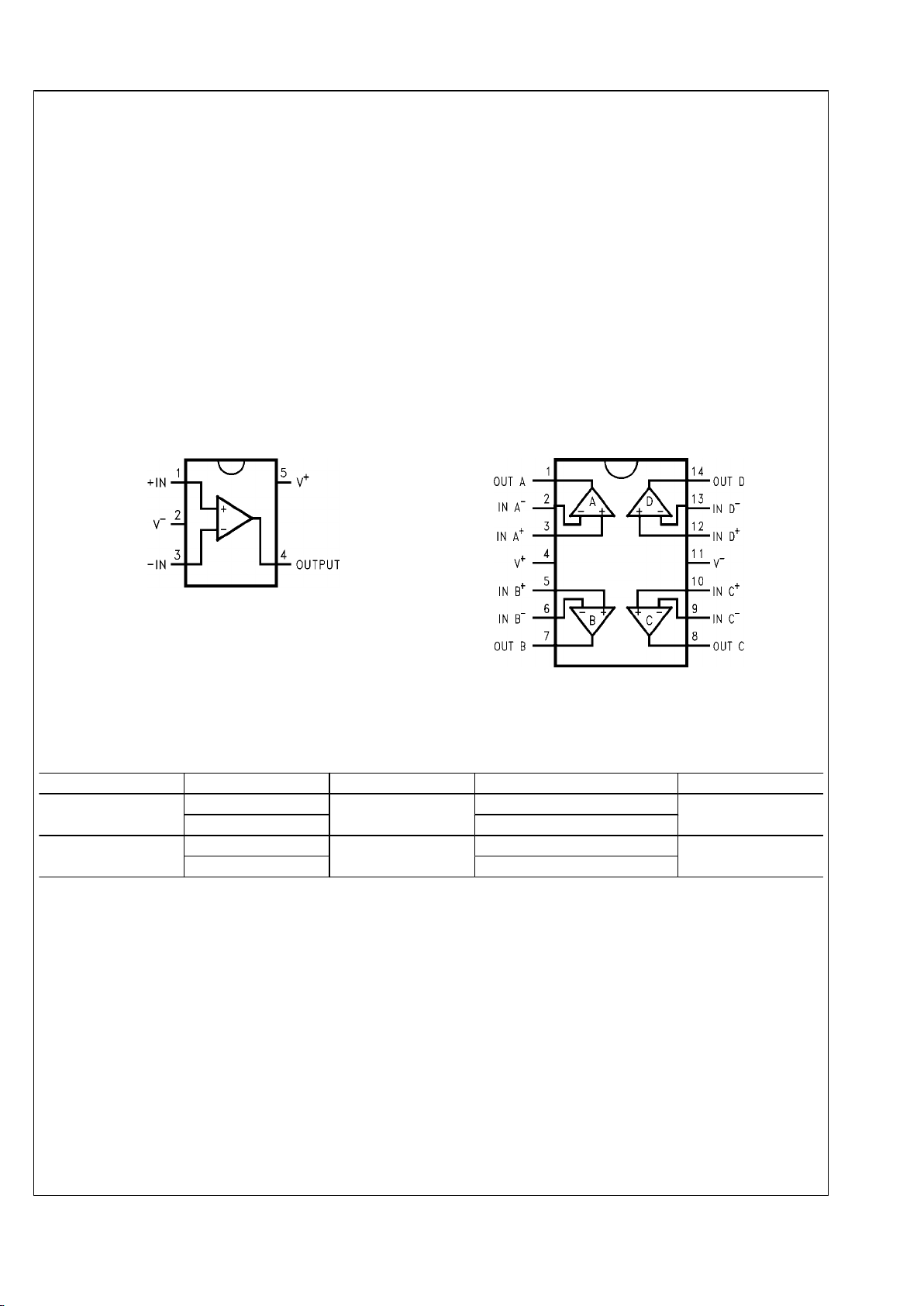
Connection Diagrams
5-Pin SC70
20168302
Top View
14–Pin TSSOP
20168304
Top View
Ordering Information
Package Part Number Package Marking Transport Media NSC Drawing
5-Pin SC70
LMV841MG
A97
1k Units Tape and Reel
MAA05A
LMV841MGX 3k Units Tape and Reel
14-Pin TSSOP
LMV844MT
LMV844MT
94 Units/Rail
MTC14
LMV844MTX 2.5k Units Tape and Reel
5 www.national.com
LMV841 Single / LMV844 Quad
Page 6
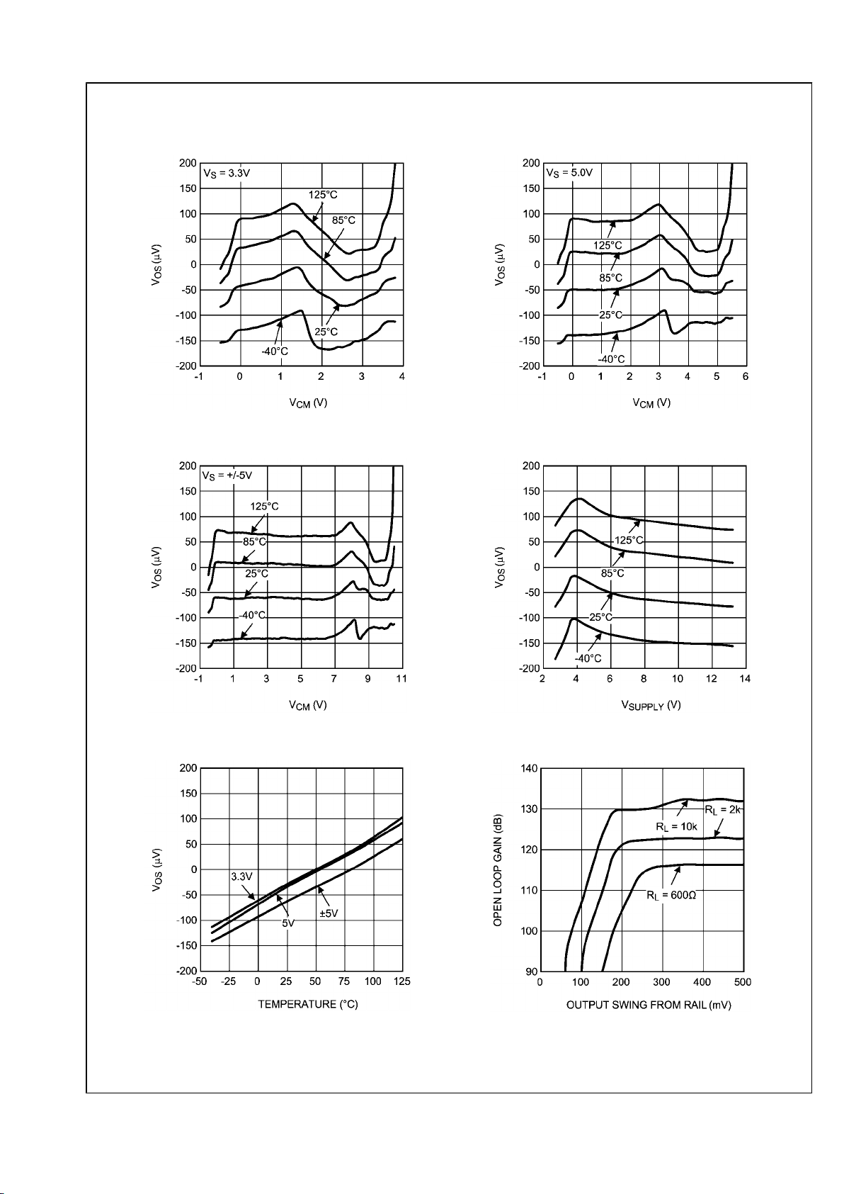
Typical Performance Characteristics At T
A
= 25°C, RL = 10 kΩ, VS = 5V. Unless otherwise specified.
VOS vs. VCM Over Temperature at 3.3V
20168310
VOS vs. VCM Over Temperature at 5.0V
20168311
V
OS
vs. VCM Over Temperature at ±5.0V
20168312
VOS vs. Supply Voltage
20168313
VOS vs. Temperature
20168314
DC Gain vs. V
OUT
20168315
www.national.com 6
LMV841 Single / LMV844 Quad
Page 7

Input Bias Current vs. V
CM
20168316
Input Bias Current vs. V
CM
20168317
Input Bias Current vs. V
CM
20168318
Supply Current vs. Supply Voltage
20168319
Sinking Current vs. Supply Voltage
20168320
Sourcing Current vs. Supply Voltage
20168321
7 www.national.com
LMV841 Single / LMV844 Quad
Page 8

Output Swing High vs. Supply Voltage RL = 2k
20168322
Output Swing High vs. Supply Voltage RL = 10k
20168323
Output Swing Low vs. Supply Voltage RL = 2k
20168324
Output Swing Low vs. Supply Voltage RL = 10k
20168325
Output Voltage Swing vs. Load Current
20168326
Open Loop Frequency Response Over Temperature
20168327
www.national.com 8
LMV841 Single / LMV844 Quad
Page 9

Open Loop Frequency Response Over Load Conditions
20168328
Phase Margin vs. C
L
20168329
PSRR vs. Frequency
20168330
CMRR vs. Frequency
20168331
Channel separation vs. Frequency
20168332
Large Signal Step Response With GAIN = 1
20168373
9 www.national.com
LMV841 Single / LMV844 Quad
Page 10

Large Signal Step Response With GAIN = 10
20168374
Small Signal Step Response With GAIN = 1
20168335
Small Signal Step Response With GAIN = 10
20168376
Overshoot vs C
L
20168338
Input Voltage Noise vs. Frequency
20168339
THD+N vs. Frequency
20168340
www.national.com 10
LMV841 Single / LMV844 Quad
Page 11

THD+N vs. V
OUT
20168341
Closed Loop Output Impedance vs. Frequency
20168343
11 www.national.com
LMV841 Single / LMV844 Quad
Page 12

Application Information
INTRODUCTION
The LMV841 and LMV844 are operational amplifiers with
near-precision specifications: low noise, low temperature
drift, low offset and rail-to-rail input and output.
The low supply current, a temperature range of −40°C to
125°C, the 12V supply with CMOS input and the small SC70
package make this a unique op amp family.
Possible applications are instrumentation, medical, test
equipment, audio and automotive applications.
The small SC70 package for the LMV841, and the low supply
current per amplifier, 1 mA, make the LMV841/LMV844 perfect choices for portable electronics.
INPUT PROTECTION
The LMV841/LMV844 have a set of anti-parallel diodes D
1
and D2 between the input pins, as shown in Figure 1. These
diodes are present to protect the input stage of the amplifier.
At the same time, they limit the amount of differential input
voltage that is allowed on the input pins.
A differential signal larger than one diode voltage drop can
damage the diodes. The differential signal between the inputs
needs to be limited to ±300 mV or the input current needs to
be limited to ±10 mA.
Note that when the op amp is slewing, a differential input voltage exists that forward biases the protection diodes. This may
result in current being drawn from the signal source. While
this current is already limited by the internal resistors R1 and
R2 (both 130Ω), a resistor of 1 kΩ can be placed in the feedback path, or a 500Ω resistor can be placed in series with the
input signal for further limitation.
20168351
FIGURE 1. Protection Diodes between the Input Pins
INPUT STAGE
The input stage of this amplifier consists of a PMOS and an
NMOS input pair to achieve a more than rail-to-rail input
range.
For input voltages close to the negative rail, only the PMOS
pair is active. Close to the positive rail, only the NMOS pair is
active.
For intermediate signals, the transition from PMOS pair to
NMOS pair will result in a very small offset shift, which appears at approximately 1V from the positive rail.
To reduce this small offset shift, the amplifier is trimmed during production, resulting in an input offset voltage of less then
0.5 mV at room temperature over the total input range.
CAPACITIVE LOAD
The LMV841/LMV844 can be connected as non-inverting unity-gain amplifiers. This configuration is the most sensitive to
capacitive loading.
The combination of a capacitive load placed on the output of
an amplifier along with the amplifier’s output impedance creates a phase lag, which reduces the phase margin of the
amplifier. If the phase margin is significantly reduced, the response will be underdamped which causes peaking in the
transfer and when there is too much peaking the op amp might
start oscillating.
In order to drive heavier capacitive loads, an isolation resistor,
R
ISO
, should be used, as shown in Figure 2. By using this
isolation resistor, the capacitive load is isolated from the
amplifier’s output, and hence, the pole caused by CL is no
longer in the feedback loop. The larger the value of R
ISO
, the
more stable the output voltage will be. If values of R
ISO
are
sufficiently large, the feedback loop will be stable, independent of the value of CL. However, larger values of R
ISO
result
in reduced output swing and reduced output current drive.
20168350
FIGURE 2. Isolating Capacitive Load
REDUCING OVERSHOOT
When the output of the op amp is at its lower swing limit (i.e.
saturated near V−), rapidly rising signals can cause some
overshoot.
This overshoot can be reduced by adding a resistor from the
output to V+. Even in extreme situations at high temperatures,
a 10k resistor is sufficient to reduce the overshoot to negligible
levels.
The resistor at the output will however reduce the maximum
output swing, as would any resistive load at the output.
DECOUPLING AND LAYOUT
Care must be given when creating the board layout for the op
amp.
For decoupling the supply lines it is suggested that 10 nF capacitors be placed as close as possible to the op amp.
For single supply, place a capacitor between V+ and V−. For
dual supplies, place one capacitor between V+ and the board
ground, and the second capacitor between ground and V−.
NOISE DUE TO RESISTORS
The LMV841/LMV844 have good noise specifications, and
will frequently be used in low-noise applications. Therefore it
is important to take into account the influence of the resistors
on the total noise contribution.
For applications with a voltage input configuration it is, in general, beneficial to keep the resistor values low. In these configurations high resistor values mean high noise levels.
www.national.com 12
LMV841 Single / LMV844 Quad
Page 13

However, using low resistor values will increase the power
consumption of the application. This is not always acceptable
for portable applications.
To determine if the noise is acceptable for the application, use
the following formula for resistor noise :
where:
eth = Thermal noise voltage (Vrms)
k = Boltzmann constant (1.38 x 10⁻²³ J/K)
T = Absolute temperature (K)
R = Resistance (Ω)
B = Noise bandwidth (Hz), fmax - fmin
Given in an example with a resistor of 1MΩ at 25°C (298 K)
over a frequency range of 100 kHz:
To keep the noise of the application low it might be necessary
to decrease the resistors to 100k, which will decrease the
noise to –97.8 dBV (12.8 uV).
The op amp's input-referred noise of 20 nV/ at 1 kHz is
equivalent to the noise of a 24 kΩ resistor.
ACTIVE FILTER
The rail-to-rail input and output of the LMV841/LMV844 and
the wide supply voltage range make these amplifiers ideal to
use in numerous applications. One of the typical applications
is an active filter as shown in Figure 3. This example is a bandpass filter, for which the pass band is widened. This is
achieved by cascading two band-pass filters, with slightly different center frequencies.
20168358
FIGURE 3. Active Filter
The center frequency of the separate band-pass filters can be
calculated by:
In this example a filter was designed with its pass band at 10
kHz. The two separate band-pass filters are designed to have
a center frequency of approximately 10% from the frequency
of the total filter:
C = 33 nF
R1 = 2 kΩ
R2 = 6.2 kΩ
R3 = 45 Ω
This will give for filter A:
And for filter B with C = 27 nF:
Bandwidth can be calculated by:
For filter A this will give
and for filter B:
The response of the two filters and the combined filter is
shown in Figure 4.
20168359
FIGURE 4. Active Filter Curve
13 www.national.com
LMV841 Single / LMV844 Quad
Page 14

The filter responses of filter A and filter B are shown as the
thin lines in Figure 4, the response of the combined filter is
shown as the thick line. Shifting the center frequencies of the
separate filters farther apart, will result in a wider band, however positioning the center frequencies too far apart will result
in a less flat gain within the band. For wider bands more bandpass filters can be cascaded.
Tip: Use the WEBENCH internet tools at www.national.com
for your filter application.
HIGH-SIDE CURRENT SENSING
The rail-to-rail input and the low VOS features make the
LMV841/844 ideal op amps for high-side current sensing application.
To measure a current, a sense resistor is placed in series with
the load, as shown in Figure 5. The current flowing through
this sense resistor will result in a voltage drop, that is amplified
by the op amp.
Suppose we need to measure a current between 0A and 2A
using a sense resistor of 100 mΩ, and convert it to an output
voltage of 0 to 5V. A current of 2A flowing through the load
and the sense resistor will result in a voltage of 200 mV across
the sense resistor. The op amp will amplify this 200 mV to fit
the current range to the output voltage range. We can use the
formula:
V
OUT
= RF / RG * V
SENSE
to calculate the gain needed. For a load current of 2A and an
output voltage of 5V the gain would be V
OUT
/ V
SENSE
= 25.
When we use a feedback resistor, RF, of 100 kΩ the value for
RG would be 4 kΩ. The tolerance of the resistors has to be
low to obtain a good common-mode rejection.
20168371
FIGURE 5. High-Side Current Sensing
HIGH IMPEDANCE SENSOR INTERFACE
With CMOS inputs, the LMV841/LMV844 are particularly suited to be used as high impedance sensor interfaces.
Many sensors have high source impedances that may range
up to 10 MΩ. The input bias current of an amplifier will load
the output of the sensor, and thus cause a voltage drop across
the source resistance, as shown in Figure 6. When an op amp
is selected with a relatively high input bias current, this error
may be unacceptable.
The low input current of the LMV841/LMV844 significantly reduces such errors. The following examples show the difference between a standard op amp input and the CMOS input
of the LMV841/LMV844.
The voltage at the input of the op amp can be calculated by
V
IN+
= VS - IB * R
S
For a standard op amp the input bias Ib could be 10 nA. When
the sensor generates a signal of 1V (VS) and the sensors
impedance is 10 MΩ (RS), the signal at the op amp input will
be
VIN = 1V - 10 nA * 10 MΩ = 1V - 0.1V = 0.9V
For the CMOS input of the LMV841/LMV844, which has an
input bias current of only 0.3 pA, this would give
VIN = 1V – 0.3 pA * 10 MΩ = 1V - 3 μV = 0.999997 V !
The conclusion is that a standard op amp, with its high input
bias current input, is not a good choice for use in impedance
sensor applications. The LMV841/LMV844, in contrast, are
much more suitable due to the low input bias current. The
error is negligibly small, therefore the LMV841/LMV844 are a
must for use with high impedance sensors.
20168352
FIGURE 6. High Impedance Sensor Interface
THERMOCOUPLE AMPLIFIER
The following is a typical example for a thermocouple amplifier application with an LMV841/LMV844. A thermocouple
senses a temperature and converts it into a voltage. This signal is then amplified by the LMV841. An ADC can then convert
the amplified signal to a digital signal. For further processing
the digital signal can be processed by a microprocessor and
can be used to display or log the temperature, or use the
temperature data in a fabrication process.
Characteristics of a Thermocouple
A thermocouple is a junction of two different metals. These
metals produce a small voltage that increases with temperature.
The thermocouple used in this application is a K-type thermocouple. A K-type thermocouple is a junction between Nickel-Chromium and Nickel-Aluminum. This type is one of the
most commonly used thermocouples. There are several reasons for using the K-type thermocouple. These include temperature range, the linearity, the sensitivity and the cost.
A K-type thermocouple has a wide temperature range. The
range of this thermocouple is from approximately −200°C to
approximately 1200°C, as can be seen in Figure 7. This cov-
ers the generally used temperature ranges.
Over the main part of the range the behavior is linear. This is
important for converting the analog signal to a digital signal.
The K-type thermocouple has good sensitivity when compared to many other types, the sensitivity is 41 uV/°C. Lower
sensitivity requires more gain and makes the application more
sensitive to noise.
In addition, a K-type thermocouple is not expensive, many
other thermocouples consist of more expensive materials or
are more difficult to produce.
www.national.com 14
LMV841 Single / LMV844 Quad
Page 15

20168370
FIGURE 7. K-Type Thermocouple Response
Thermocouple Example
Suppose the range we are interested in for this example is
from 0°C to 500°C, and the resolution needed is 0.5°C. The
power supply for both the LMV841 and the ADC is 3.3V.
The temperature range of 0°C to 500°C results in a voltage
range from 0 mV to 20.6 mV produced by the thermocouple.
This is shown in Figure 7
To obtain the best accuracy the full ADC range of 0 to 3.3V is
used.
We can calculate the gain we need for the full input range of
the ADC : AV = 3.3V / 0.0206V = 160.
When we use 2 kΩ for RG, we can calculate the value for R
F
with this gain of 160. We can use AV = RF / RG to calculate
the gain, so we can calculate RF by using RF = AV x RG = 160
x 2 kΩ = 320 kΩ.
To get a resolution of 0.5°C we need a step smaller then the
minimum resolution, this means we need at least 1000 steps
(500°C / 0.5°C). A 10-bit ADC would be sufficient as this will
give us 1024 steps. This could be a 10 bit ADC like the two
channel 10-bit ADC102S021.
Unwanted Thermocouple Effect
At the point where the thermocouple wires are connected to
the circuit, usually copper wires or traces, an unwanted thermocouple effect will occur.
At this connection, this could be the connector on a PCB, the
thermocouple wiring forms a second thermocouple with the
connector. This second thermocouple disturbs the measurements from the intended thermocouple.
We can compensate for this thermocouple effect by using an
isothermal block as a reference. An isothermal block is a good
heat conductor. This means that the two thermocouple connections both have the same temperature. We can now measure the temperature of the isothermal block, and thereby the
temperature of the thermocouple connections. This is usually
called the cold junction reference temperature.
In the example, an LM35 is used to measure this temperature.
This semiconductor temperature sensor can accurately measure temperatures from −55°C to 150°C.
The ADC in this example also coverts the signal from the
LM35 to a digital signal. Now the microprocessor can compensate the amplified thermocouple signal, for the unwanted
thermocouple effect.
20168353
FIGURE 8. Thermocouple Amplifier
15 www.national.com
LMV841 Single / LMV844 Quad
Page 16

Physical Dimensions inches (millimeters) unless otherwise noted
5-Pin SC70
NS Package Number MAA05A
14–Pin TSSOP
NS Package Number MTC14
www.national.com 16
LMV841 Single / LMV844 Quad
Page 17

Notes
17 www.national.com
LMV841 Single / LMV844 Quad
Page 18

Notes
LMV841 Single / LMV844 Quad CMOS Input, RRIO, Wide Supply Range Operational Amplifiers
THE CONTENTS OF THIS DOCUMENT ARE PROVIDED IN CONNECTION WITH NATIONAL SEMICONDUCTOR CORPORATION
(“NATIONAL”) PRODUCTS. NATIONAL MAKES NO REPRESENTATIONS OR WARRANTIES WITH RESPECT TO THE ACCURACY
OR COMPLETENESS OF THE CONTENTS OF THIS PUBLICATION AND RESERVES THE RIGHT TO MAKE CHANGES TO
SPECIFICATIONS AND PRODUCT DESCRIPTIONS AT ANY TIME WITHOUT NOTICE. NO LICENSE, WHETHER EXPRESS,
IMPLIED, ARISING BY ESTOPPEL OR OTHERWISE, TO ANY INTELLECTUAL PROPERTY RIGHTS IS GRANTED BY THIS
DOCUMENT.
TESTING AND OTHER QUALITY CONTROLS ARE USED TO THE EXTENT NATIONAL DEEMS NECESSARY TO SUPPORT
NATIONAL’S PRODUCT WARRANTY. EXCEPT WHERE MANDATED BY GOVERNMENT REQUIREMENTS, TESTING OF ALL
PARAMETERS OF EACH PRODUCT IS NOT NECESSARILY PERFORMED. NATIONAL ASSUMES NO LIABILITY FOR
APPLICATIONS ASSISTANCE OR BUYER PRODUCT DESIGN. BUYERS ARE RESPONSIBLE FOR THEIR PRODUCTS AND
APPLICATIONS USING NATIONAL COMPONENTS. PRIOR TO USING OR DISTRIBUTING ANY PRODUCTS THAT INCLUDE
NATIONAL COMPONENTS, BUYERS SHOULD PROVIDE ADEQUATE DESIGN, TESTING AND OPERATING SAFEGUARDS.
EXCEPT AS PROVIDED IN NATIONAL’S TERMS AND CONDITIONS OF SALE FOR SUCH PRODUCTS, NATIONAL ASSUMES NO
LIABILITY WHATSOEVER, AND NATIONAL DISCLAIMS ANY EXPRESS OR IMPLIED WARRANTY RELATING TO THE SALE
AND/OR USE OF NATIONAL PRODUCTS INCLUDING LIABILITY OR WARRANTIES RELATING TO FITNESS FOR A PARTICULAR
PURPOSE, MERCHANTABILITY, OR INFRINGEMENT OF ANY PATENT, COPYRIGHT OR OTHER INTELLECTUAL PROPERTY
RIGHT.
LIFE SUPPORT POLICY
NATIONAL’S PRODUCTS ARE NOT AUTHORIZED FOR USE AS CRITICAL COMPONENTS IN LIFE SUPPORT DEVICES OR
SYSTEMS WITHOUT THE EXPRESS PRIOR WRITTEN APPROVAL OF THE CHIEF EXECUTIVE OFFICER AND GENERAL
COUNSEL OF NATIONAL SEMICONDUCTOR CORPORATION. As used herein:
Life support devices or systems are devices which (a) are intended for surgical implant into the body, or (b) support or sustain life and
whose failure to perform when properly used in accordance with instructions for use provided in the labeling can be reasonably expected
to result in a significant injury to the user. A critical component is any component in a life support device or system whose failure to perform
can be reasonably expected to cause the failure of the life support device or system or to affect its safety or effectiveness.
National Semiconductor and the National Semiconductor logo are registered trademarks of National Semiconductor Corporation. All other
brand or product names may be trademarks or registered trademarks of their respective holders.
Copyright© 2007 National Semiconductor Corporation
For the most current product information visit us at www.national.com
National Semiconductor
Americas Customer
Support Center
Email:
new.feedback@nsc.com
Tel: 1-800-272-9959
National Semiconductor Europe
Customer Support Center
Fax: +49 (0) 180-530-85-86
Email: europe.support@nsc.com
Deutsch Tel: +49 (0) 69 9508 6208
English Tel: +49 (0) 870 24 0 2171
Français Tel: +33 (0) 1 41 91 8790
National Semiconductor Asia
Pacific Customer Support Center
Email: ap.support@nsc.com
National Semiconductor Japan
Customer Support Center
Fax: 81-3-5639-7507
Email: jpn.feedback@nsc.com
Tel: 81-3-5639-7560
www.national.com
 Loading...