

Page 1
August 1999
LMV821 Single/ LMV822 Dual/ LMV824 Quad
Low Voltage, Low Power, R-to-R Output, 5 MHz Op Amps
General Description
The LMV821/LMV822/LMV824 bring performance and
economy to low voltage / low power systems. Witha5MHz
unity-gain frequency and a guaranteed 1.4 V/µs slew rate,
the quiescent current is only 220 µA/amplifier (2.7 V). They
provide rail-to-rail (R-to-R) output swing into heavy loads
(600 ΩGuarantees). The input common-mode voltage range
includes ground, and the maximum input offset voltage is
3.5mV (Guaranteed). They are also capable of comfortably
driving large capacitive loads (refer to the application notes
section).
The LMV821 (single) is available in the ultra tiny SC70-5
package, which is about half the size of the previous title
holder, the SOT23-5.
Overall, the LMV821/LMV822/LMV824 (Single/Dual/Quad)
are low voltage, low power, performance op amps, that can
be designed into a wide range of applications, at an economical price.
Features
(For Typical, 5 V Supply Values; Unless Otherwise Noted)
n Ultra Tiny, SC70-5 Package 2.0 x 2.0 x 1.0 mm
n Guaranteed 2.5 V, 2.7 V and 5 V Performance
n Maximum VOS 3.5 mV (Guaranteed)
n VOS Temp. Drift 1 uV/˚ C
n GBW product
n I
Supply
n Minimum SR 1.4 V/us (Guaranteed)
n CMRR 90 dB
n PSRR 85 dB
n Rail-to-Rail (R-to-R) Output Swing
@
—
600 Ω Load 160 mV from rail
@
—
10 kΩ Load 55 mV from rail
n V
CM
n Stable with High Capacitive Loads (Refer to Application
Section)
@
@
@
2.7 V 5 MHz
2.7 V 220 µA/Amplifier
5 V -0.3 V to 4.3 V
Applications
n Cordless Phones
n Cellular Phones
n Laptops
n PDAs
n PCMCIA
LMV821 Single/ LMV822 Dual/ LMV824 Quad Low Voltage, Low Power, RRO, 5 MHz Op Amps
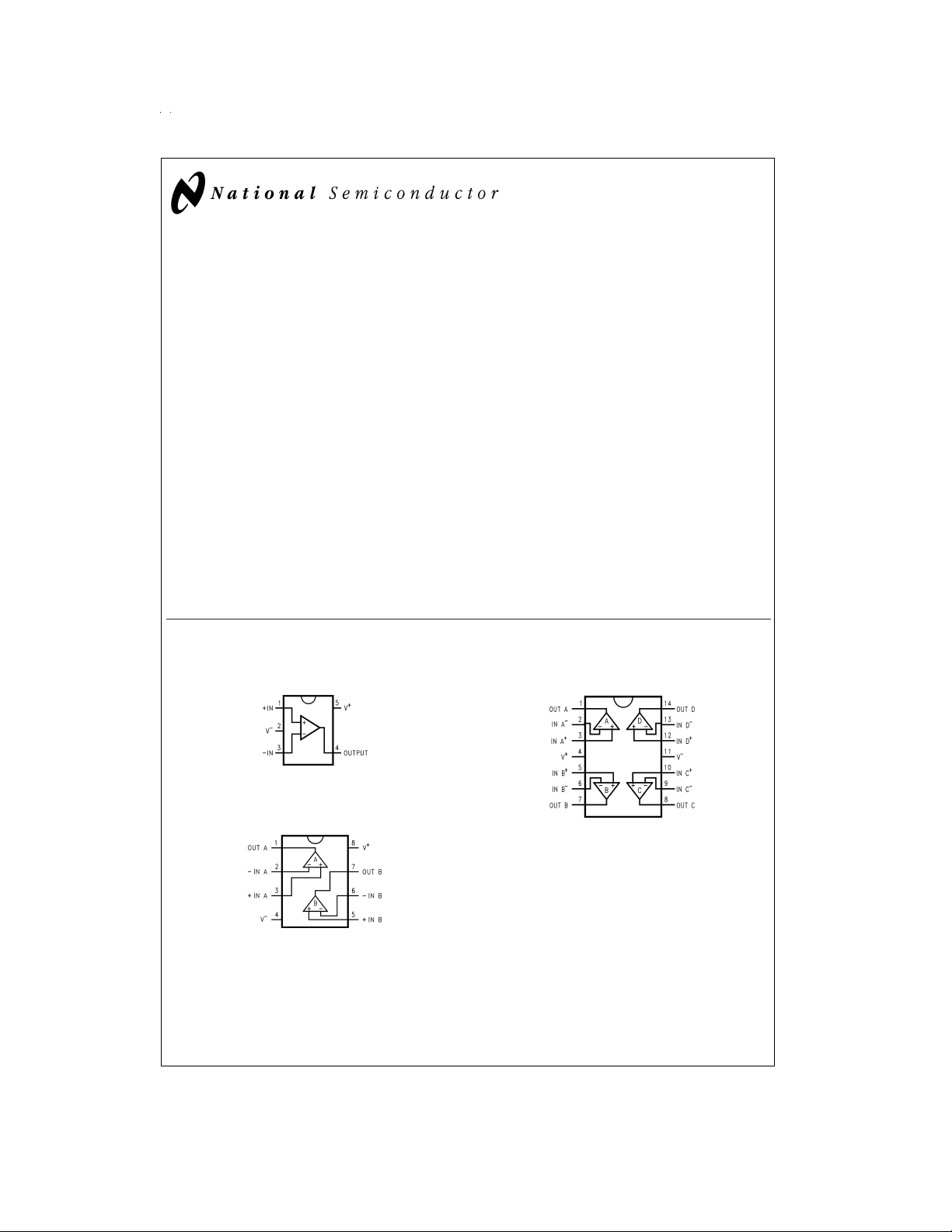
Connection Diagrams
5-Pin SC70-5/SOT23-5
DS100128-84
Top View
8-Pin SO/MSOP
DS100128-63
Top View
© 1999 National Semiconductor Corporation DS100128 www.national.com
14-Pin SO/TSSOP
DS100128-85
Top View
Page 2
Ordering Information
Temperature Range
Package
−40˚C to +85˚C
5-Pin SC-70-5 LMV821M7 A15 1k Units Tape and Reel MAA05
LMV821M7X A15 3k Units Tape and Reel
5-Pin SOT23-5 LMV821M5 A14 1k UnitsTape and Reel MA05B
LMV821M5X A14 3k Units Tape and Reel
8-Pin SO LMV822M LMV822M Rails M08A
LMV822MX LMV822M 2.5k Units Tape and
8-Pin MSOP LMV822MM LMV822 1k Units Tape and Reel MUA08A
LMV822MMX LMV822 3.5k Units Tape and
14-Pin SO LMV824M LMV824M Rails M14A
LMV824MX LMV824M 2.5k Units Tape and
14-Pin TSSOP LMV824MT LMV824MT Rails MTC14
LMV824MTX LMV824MT 2.5k Units Tape and
Packaging Marking Transport Media NSC DrawingIndustrial
Reel
Reel
Reel
Reel
www.national.com 2
Page 3
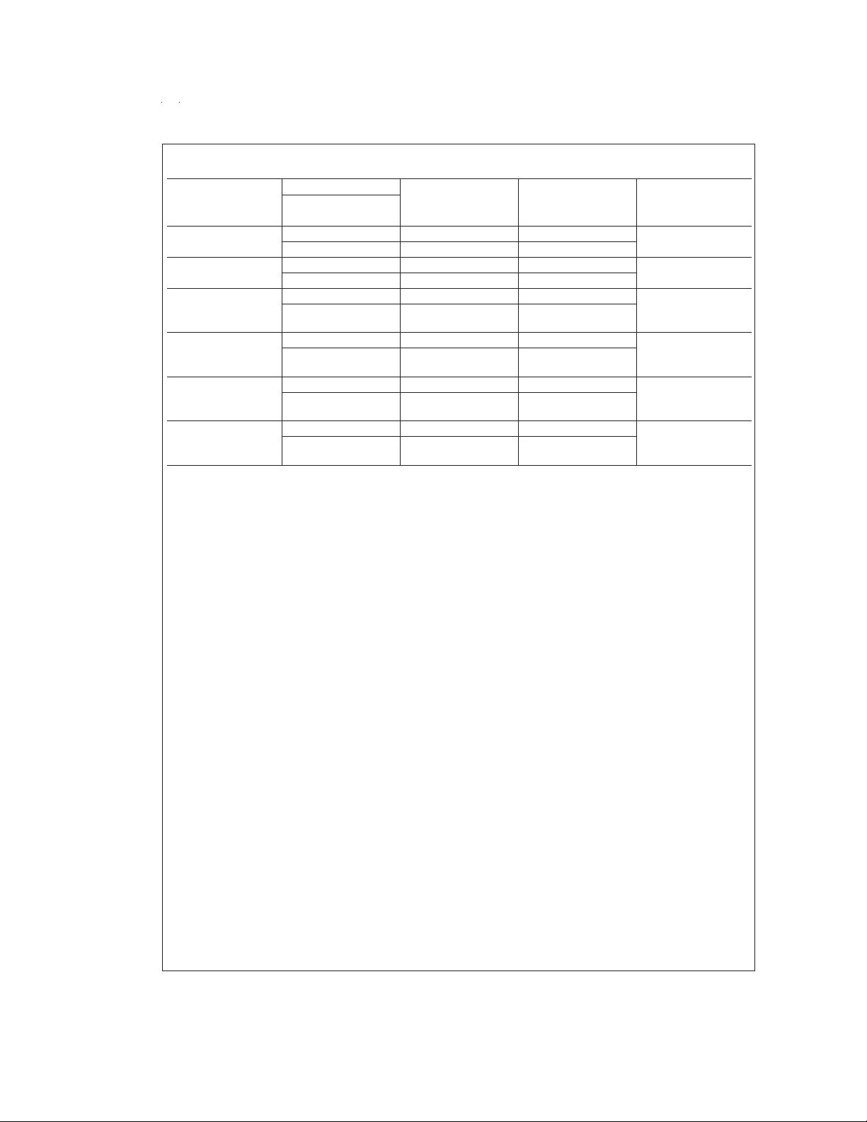
Absolute Maximum Ratings (Note 1)
If Military/Aerospace specified devices are required,
please contact the National Semiconductor Sales Office/
Distributors for availability and specifications.
ESD Tolerance (Note 2)
Machine Model 100V
Human Body Model
LMV822/824 2000V
LMV821 1500V
Differential Input Voltage
Supply Voltage (V
Output Short Circuit to V
Output Short Circuit to V
+–V−
) 5.5V
+
(Note 3)
−
(Note 3)
Soldering Information
Infrared or Convection (20 sec) 235˚C
Storage Temperature Range −65˚C to 150˚C
±
Supply Voltage
Operating Ratings (Note 1)
Supply Voltage 2.5V to 5.5V
Temperature Range
LMV821, LMV822, LMV824 −40˚C ≤T
Thermal Resistance (θ
Ultra Tiny SC70-5 Package
5-Pin Surface Mount
Tiny SOT23-5 Package 5-Pin
Surface Mount
SO Package, 8-Pin Surface
Mount 190 ˚C/W
MSOP Package, 8-Pin Mini
Surface Mount 235 ˚C/W
SO Package, 14-Pin Surface
Mount 145 ˚C/W
TSSOP Package, 14-Pin 155 ˚C/W
)
JA
Junction Temperature (Note 4) 150˚C
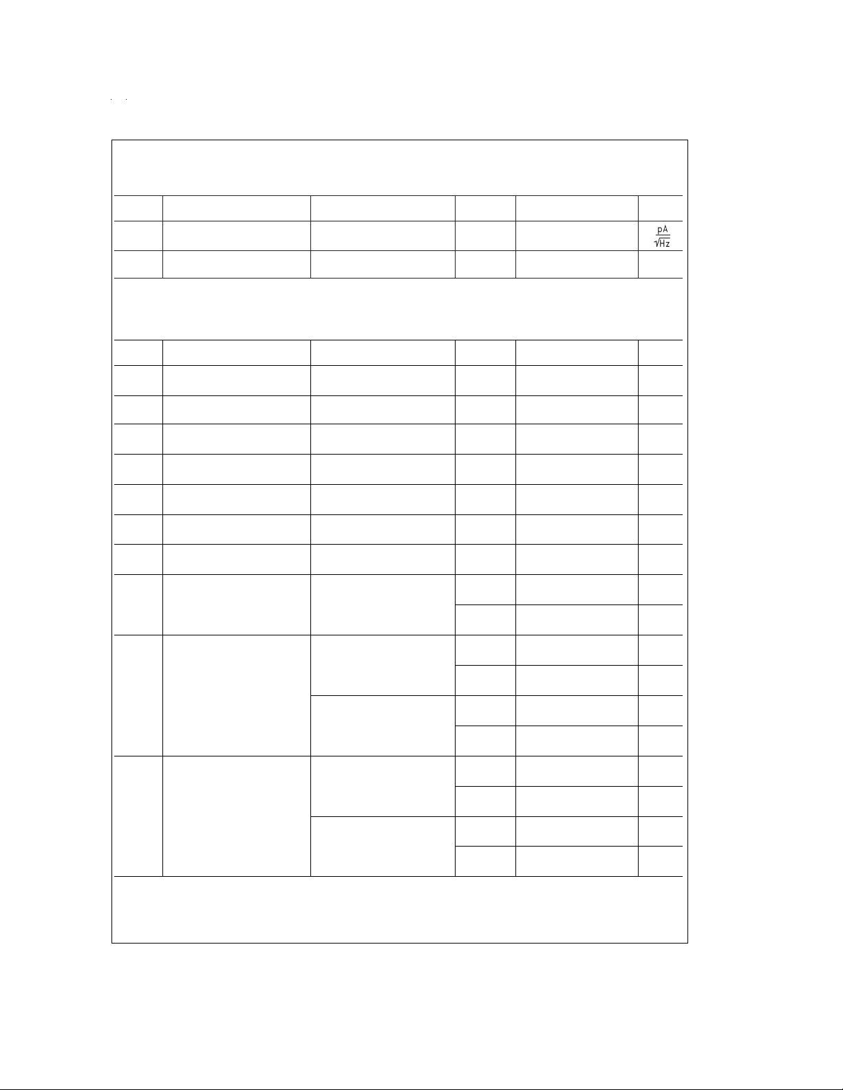
2.7V DC Electrical Characteristics
Unless otherwise specified, all limits guaranteed for TJ= 25˚C. V+= 2.7V, V−= 0V, VCM= 1.0V, VO= 1.35V and R
Boldface limits apply at the temperature extremes.
Symbol Parameter Condition
V
OS
TCV
I
B
I
OS
CMRR Common Mode Rejection Ratio 0V ≤ V
+PSRR Positive Power Supply
−PSRR Negative Power Supply
V
CM
A
V
Input Offset Voltage 1 3.5 mV
Input Offset Voltage Average
OS
Drift
Input Bias Current 30 90 nA
Input Offset Current 0.5 30 nA
≤ 1.7V 85 70 dB
CM
+
Rejection Ratio
Rejection Ratio
Input Common-Mode Voltage
1.7V ≤ V
0V, V
-1.0V ≤ V
V
For CMRR ≥ 50dB -0.3 -0.2 V
≤ 4V, V-= 1V, VO=
=0V
CM
-
≤ -3.3V, V+=1.7V,
= 0V, VCM=0V
O
Range
Large Signal Voltage Gain Sourcing, RL=600Ω to 1.35V,
=1.35V to 2.2V
V
O
Sinking, R
V
O
Sourcing, R
V
O
Sinking, R
V
O
=600Ω to 1.35V,
L
=1.35V to 0.5V
=2kΩ to 1.35V,
L
=1.35V to 2.2V
=2kΩ to 1.35,
L
=1.35 to 0.5V
Typ
(Note 5)
1 µV/˚C
85 75 dB
85 73 dB
2.0 1.9 V
100 90 dB
90 85 dB
100 95 dB
95 90 dB
LMV821/822/824
Limit (Note 6)
4 max
140 max
50 max
68 min
70 min
70 min
85 min
80 min
90 min
85 min
J
440 ˚C/W
265 ˚C/W
>
L
≤85˚C
1MΩ.
Units
max
min
www.national.com3
Page 4
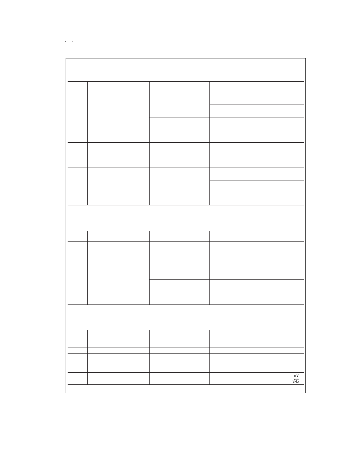
2.7V DC Electrical Characteristics (Continued)
Unless otherwise specified, all limits guaranteed for TJ= 25˚C. V+= 2.7V, V−= 0V, VCM= 1.0V, VO= 1.35V and R
Boldface limits apply at the temperature extremes.
Symbol Parameter Condition
V
O
I
O
I
S
Output Swing V+=2.7V, RL= 600Ω to 1.35V 2.58 2.50 V
+
V
=2.7V, RL=2kΩto 1.35V 2.66 2.60 V
Output Current Sourcing, VO=0V 16 12 mA
Sinking, V
=2.7V 26 12 mA
O
Supply Current LMV821 (Single) 0.22 0.3 mA
LMV822 (Dual) 0.45 0.6 mA
LMV824 (Quad) 0.72 1.0 mA
Typ
(Note 5)
0.13 0.20 V
0.08 0.120 V
LMV821/822/824
Limit (Note 6)
2.40 min
0.30 max
2.50 min
0.200 max
0.5 max
0.8 max
1.2 max
L
>
1MΩ.
Units
min
min
2.5V DC Electrical Characteristics
Unless otherwise specified, all limits guaranteed for TJ= 25˚C. V+= 2.5V, V−= 0V, VCM= 1.0V, VO= 1.25V and R
Boldface limits apply at the temperature extremes.
Symbol Parameter Condition
V
OS
Input Offset Voltage 1 3.5 mV
Typ
(Note 5)
LMV821/822/824
Limit (Note 6)
4 max
V
O
Output Swing V+=2.5V, RL= 600Ω to 1.25V 2.37 2.30 V
2.20 min
0.13 0.20 V
0.30 max
+
V
=2.5V, RL=2kΩto 1.25V 2.46 2.40 V
2.30 min
0.08 0.12 V
0.20 max
L
>
1MΩ.
Units
2.7V AC Electrical Characteristics
Unless otherwise specified, all limits guaranteed for TJ= 25˚C. V+= 2.7V, V−= 0V, VCM= 1.0V, VO= 1.35V and R
Boldface limits apply at the temperature extremes.
Symbol Parameter Conditions
Typ
(Note 5)
LMV821/822/824 Limit
(Note 6)
SR Slew Rate (Note 7) 1.5 V/µs
GBW Gain-Bandwdth Product 5 MHz
Φ
m
G
m
Phase Margin 61 Deg.
Gain Margin 10 dB
Amp-to-Amp Isolation (Note 8) 135 dB
e
n
Input-Related Voltage Noise f = 1 kHz, VCM=1V 28
L
>
1MΩ.
Units
www.national.com 4
Page 5
2.7V AC Electrical Characteristics (Continued)
Unless otherwise specified, all limits guaranteed for TJ= 25˚C. V+= 2.7V, V−= 0V, VCM= 1.0V, VO= 1.35V and R
Boldface limits apply at the temperature extremes.
Symbol Parameter Conditions
i
n
Input-Referred Current Noise f = 1 kHz 0.1
Typ
(Note 5)
LMV821/822/824 Limit
(Note 6)
L
>
1MΩ.
Units
THD Total Harmonic Distortion f = 1 kHz, AV= −2,
=10kΩ,VO= 4.1 V
R
L
PP
0.01
5V DC Electrical Characteristics
Unless otherwise specified, all limits guaranteed for TJ= 25˚C. V+= 5V, V−= 0V, VCM= 2.0V, VO= 2.5V and R
Boldface limits apply at the temperature extremes.
Symbol Parameter Condition
V
OS
TCV
I
B
I
OS
CMRR Common Mode Rejection Ratio 0V ≤ V
+PSRR Positive Power Supply
−PSRR Negative Power Supply
V
CM
A
V
V
O
Input Offset Voltage 1 3.5 mV
Input Offset Voltage Average
OS
Drift
Input Bias Current 40 100 nA
Input Offset Current 0.5 30 nA
≤ 4.0V 90 72 dB
CM
+
Rejection Ratio
Rejection Ratio
Input Common-Mode Voltage
1.7V ≤ V
0V, V
-1.0V ≤ V
V
For CMRR ≥ 50dB -0.3 -0.2 V
≤ 4V, V-= 1V, VO=
=0V
CM
-
≤ -3.3V, V+=1.7V,
= 0V, VCM=0V
O
Range
Large Signal Voltage Gain Sourcing, RL=600Ω to 2.5V,
=2.5 to 4.5V
V
O
Sinking, R
V
O
Sourcing, R
V
O
Sinking, R
V
O
=600Ω to 2.5V,
L
=2.5 to 0.5V
L
=2.5 to 4.5V
=2kΩ to 2.5,
L
=2.5 to 0.5V
=2kΩ to 2.5V,
Output Swing V+=5V,RL= 600Ω to 2.5V 4.84 4.75 V
+
V
=5V, RL=2kΩ to 2.5V 4.90 4.85 V
Typ
(Note 5)
1 µV/˚C
85 75 dB
85 73 dB
4.3 4.2 V
105 95 dB
105 95 dB
105 95 dB
105 95 dB
0.17 0.250 V
0.10 0.15 V
LMV821/822/824
Limit (Note 6)
4.0 max
150 max
50 max
70 min
70 min
70 min
90 min
90 min
90 min
90 min
4.70 min
.30 max
4.80 min
0.20 max
L
>
%
1MΩ.
Units
max
min
www.national.com5
Page 6
5V DC Electrical Characteristics (Continued)
Unless otherwise specified, all limits guaranteed for TJ= 25˚C. V+= 5V, V−= 0V, VCM= 2.0V, VO= 2.5V and R
Boldface limits apply at the temperature extremes.
Symbol Parameter Condition
I
O
I
S
Output Current Sourcing, VO=0V 45 20 mA
Sinking, V
=5V 40 20 mA
O
Supply Current LMV821 (Single) 0.30 0.4 mA
LMV822 (Dual) 0.5 0.7 mA
LMV824 (Quad) 1.0 1.3 mA
Typ
(Note 5)
LMV821/822/824
Limit (Note 6)
15 min
15 min
0.6 max
0.9 max
1.5 max
L
>
1MΩ.
Units
5V AC Electrical Characteristics
Unless otherwise specified, all limits guaranteed for TJ= 25˚C. V+= 5V, V−= 0V, VCM= 2V, VO= 2.5V and R
Boldface limits apply at the temperature extremes.
Symbol Parameter Conditions
Typ
(Note 5)
LMV821/822/824 Limit
(Note 6)
SR Slew Rate (Note 7) 2.0 1.4 V/µs
GBW Gain-Bandwdth Product 5.6 MHz
Φ
m
G
m
Phase Margin 67 Deg.
Gain Margin 15 dB
Amp-to-Amp Isolation (Note 8) 135 dB
e
n
i
n
THD Total Harmonic Distortion f = 1 kHz, AV= −2,
Note 1: Absolute Maximum Ratings indicate limits beyond which damage to the device may occur.Operating Ratings indicate conditions for which the device is intended to be functional, but specific performance is not guaranteed. For guaranteed specifications and the test conditions, see the Electrical Characteristics.
Note 2: Human body model, 1.5 kΩ in series wth 100 pF. Machine model, 200Ω in series with 100 pF.
Note 3: Applies to both single-supply and split-supply operation. Continuous short circuit operation at elevated ambient temperature can result in exceeding the
maximum allowed junction temperature of 150˚C. Output currents in excess of 45 mA over long term may adversely affect reliability.
Note 4: The maximum power dissipation is a function of T
(max)
Note 5: Typical Values represent the most likely parametric norm.
Note 6: All limits are guaranteed by testing or statistical analysis.
Note 7: V
Note 8: Input referred, V
Input-Related Voltage Noise f = 1 kHz, VCM=1V 24
Input-Referred Current Noise f = 1 kHz 0.25
=10kΩ,VO= 4.1 V
R
L
, θJA, and TA. The maximum allowable power dissipation at any ambient temperature is PD=(T
–TA)/θJA. All numbers apply for packages soldered directly into a PC board.
+
= 5V. Connected as voltage follower with 3V step input. Number specified is the slower of the positive and negative slew rates.
+
= 5V and RL= 100 kΩ connected to 2.5V. Each amp excited in turn with 1 kHz to produce VO=3VPP.
J(max)
PP
0.01
L
>
1MΩ.
Units
min
%
-
J
www.national.com 6
Page 7
5V AC Electrical Characteristics (Continued)
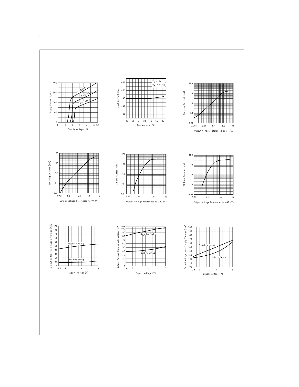
Typical Performance Characteristics Unless otherwise specified, V
Supply Current vs Supply Voltage
(LMV821)
DS100128-1
Sourcing Current vs Output
Voltage (V
S
=5V)
DS100128-4
Input Current vs Temperature
DS100128-2
Sinking Current vs Output Voltage
(V
=2.7V)
S
DS100128-5
Sourcing Current vs Output
Voltage (V
Sinking Current vs Output Voltage
(V
= +5V, single supply, TA= 25˚C.
S
=2.7V)
S
DS100128-3
=5V)
S
DS100128-6
Output Voltage Swing vs Supply
Voltage (R
=10kΩ)
L
DS100128-7
Output Voltage Swing vs Supply
Voltage (R
=2kΩ)
L
DS100128-86
Output Voltage Swing vs Supply
Voltage (R
=600Ω)
L
DS100128-8
www.national.com7
Page 8
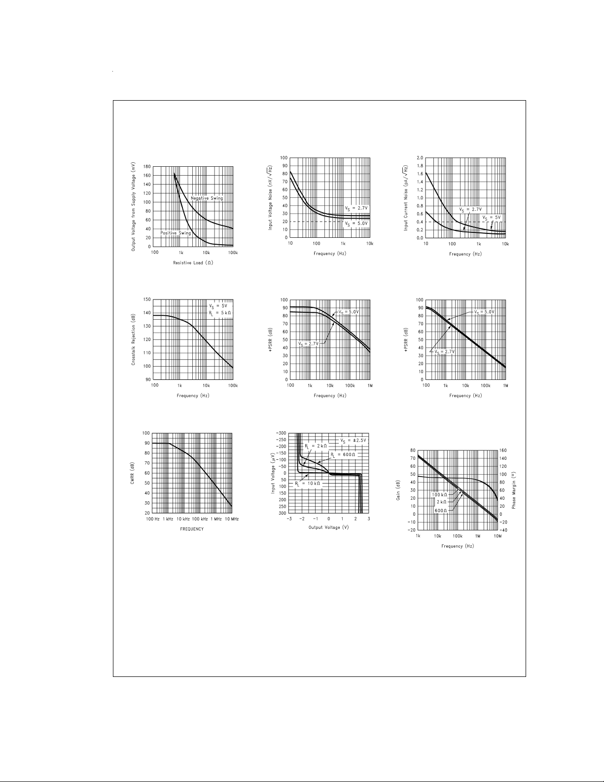
Typical Performance Characteristics Unless otherwise specified, V
T
= 25˚C. (Continued)
A
= +5V, single supply,
S
Output Voltage Swing vs Load
Resistance
DS100128-87
Crosstalk Rejection vs Frequency
DS100128-93
CMRR vs Frequency
Input Voltage Noise vs Frequency
DS100128-18
+PSRR vs Frequency
DS100128-9
Input Voltage vs Output Voltage
Input Current Noise vs Frequency
DS100128-17
-PSRR vs Frequency
DS100128-10
Gain and Phase Margin vs
Frequency (R
2.7V
=100kΩ,2kΩ, 600Ω)
L
DS100128-47
www.national.com 8
DS100128-88
DS100128-11
Page 9

Typical Performance Characteristics Unless otherwise specified, V
T
= 25˚C. (Continued)
A
Gain and Phase Margin vs
Frequency (R
5V
Gain and Phase Margin vs
Frequency (C
R
=10kΩ)2.7V
L
=100kΩ,2kΩ, 600Ω)
L
DS100128-12
=100pF, 200pF, 0pF,
L
Gain and Phase Margin vs
Frequency (Temp.=25, -40, 85˚C,
R
= 10kΩ) 2.7V
L
DS100128-13
Gain and Phase Margin vs
Frequency (C
R
=10kΩ)5V
L
=100pF,200pF,0pF
L
Gain and Phase Margin vs
Frequency (Temp.=25, -40, 85 ˚C,
R
Gain and Phase Margin vs
Frequency (C
R
= +5V, single supply,
S
=10kΩ)5V
L
=100pF,200pF,0pF
=600Ω)2.7V
L
L
DS100128-14
Gain and Phase Margin vs
Frequency (C
R
=600Ω)5V
L
=100pF,200pF,0pF
L
DS100128-15
DS100128-20
Slew Rate vs Supply Voltage
DS100128-62
DS100128-16
DS100128-19
Non-Inverting Large Signal Pulse
Response
DS100128-21
www.national.com9
Page 10

Typical Performance Characteristics Unless otherwise specified, V
T
= 25˚C. (Continued)
A
= +5V, single supply,
S
Non-Inverting Small Signal Pulse
Response
DS100128-24
THD vs Frequency
DS100128-82
Inverting Large Signal Pulse
Response
DS100128-27
Inverting Small Signal Pulse
Response
DS100128-30
www.national.com 10
Page 11

APPLICATION NOTE
This application note is divided into two sections: design
considerations and Application Circuits.
1.0 Design Considerations
This section covers the following design considerations:
1. Frequency and Phase Response Considerations
2. Unity-Gain Pulse Response Considerations
3. Input Bias Current Considerations
1.1 Frequency and Phase Response Considerations
The relationship between open-loop frequency response
and open-loop phase response determines the closed-loop
stability performance (negative feedback). The open-loop
phase response causes the feedback signal to shift towards
becoming positive feedback, thus becoming unstable. The
further the output phase angle is from the input phase angle,
the more stable the negative feedback will operate. Phase
Margin (φ
at the unity-gain crossover point. Zero degrees of phase-
) specifies this output-to-input phase relationship
m
margin means that the input and output are completely in
phase with each other and will sustain oscillation at the unitygain frequency.
The AC tables show φ
changes with load. The Gain and Phase margin vs Fre-
for a no load condition. But φ
m
quency plots in the curve section can be used to graphically
determine the φ
examine the phase angle portion of the plot, find the phase
for various loaded conditions. To do this,
m
margin point at the unity-gain frequency, and determine how
far this point is from zerodegree of phase-margin. Thelarger
the phase-margin, the more stable the circuit operation.
The bandwidth is also affected by load. The graphs of
1
and
Figure 2
fect the φ
These graphs show capacitive loads reducing both φ
provide a quick look at how various loads af-
and the bandwidth of the LMV821/822/824 family.
m
bandwidth, while resistive loads reduce the bandwidth but increase the φ
parallel with 220 picofarads capacitance, to increase the φ
. Notice how a 600Ω resistor can be added in
m
Figure
and
m
20˚(approx.), but at the price of about a 100 kHz of bandwidth.
Overall, the LMV821/822/824 family provides good stability
for loaded condition.
DS100128-61
FIGURE 2. Unity-Gain Frequency vs Common Mode
Voltage for Various Loads
1.2 Unity Gain Pulse Response Considerations
A pull-up resistor is well suited for increasing unity-gain,
pulse response stability. For example, a 600 Ω pull-up resistor reduces the overshoot voltage by about 50%, when driving a 220 pF load.
Figure 3
shows how to implement the
pull-up resistor for more pulse response stability.
m
FIGURE 3. Using a Pull-up Resistor at the Output for
Stabilizing Capacitive Loads
Higher capacitances can be driven by decreasing the value
of the pull-up resistor, but its value shouldn’t be reduced be-
m
yond the sinking capability of the part.An alternate approach
is to use an isolation resistor as illustrated in
Figure 5
shows the resulting pulse response from a LMV824,
while driving a 10,000pF load through a 20 Ω isolation
resistor.
DS100128-41
Figure 4
.
DS100128-60
FIGURE 1. Phase Margin vs Common Mode Voltage for
Various Loads
DS100128-43
FIGURE 4. Using an Isolation Resistor to Drive Heavy
Capacitive Loads
www.national.com11
Page 12

DS100128-54
FIGURE 5. Pulse Response per
Figure 4
1.3 Input Bias Current Consideration
Input bias current (I
offset voltage. This offset is primarily due to I
through the negative feedback resistor,R
is 90nA (max room) and RFis 100 kΩ, then an offset of 9 mV
will be developed (V
tor (R
), as shown in
C
input offset current (I
age in the same manner - typically 0.05 mV at room temp.
) can develop a somewhat significant
B
. For example, if I
F
OS=IBxRF
).Using a compensation resis-
Figure 6
, cancels out this affect. But the
) will still contribute to an offset volt-
OS
flowing
B
DS100128-59
FIGURE 6. Canceling the Voltage Offset Effect of Input
Bias Current
2.0 APPLICATION CIRCUITS
This section covers the following application circuits:
1. Telephone-Line Transceiver
2. “Simple” Mixer (Amplitude Modulator)
3. Dual Amplifier Active Filters (DAAFs)
a. Low-Pass Filter (LPF)
•
b. High-Pass Filter (HPF)
•
5. Tri-level Voltage Detector
2.1 Telephone-Line Transceiver
The telephone-line transceiver of
Figure 7
duplexed connection through a PCMCIA, miniature transformer. The differential configuration of receiver portion
(UR), cancels reception from the transmitter portion (UT).
Note that the input signals for the differential configuration of
UR, are the transmit voltage (Vt) and Vt/2. This is because
R
is chosen to match the coupled telephone-line imped-
match
ance; therefore dividing Vtby two (assuming R1
The differential configuration of UR has its resistors chosen
to cancel the Vt and Vt/2 inputs according to the following
equation:
B
FIGURE 7. Telephone-line Transceiver for a PCMCIA
Modem Card
Note that Cr is included for canceling outthe inadequaciesof
the lossy, miniature transformer. Refer to application note
AN-397 for detailed explanation.
2.2“Simple” Mixer (Amplitude Modulator)
The mixer of
Figure 8
is simple and provides a unique form
of amplitude modulation. Vi is the modulation frequency
(F
), while a +3V square-wave at the gate of Q1, induces a
M
carrier frequency (F
verting and non-inverting unity gain configurations. Offset-
). Q1 switches (toggles) U1 between in-
C
ting a sine wave above ground at Vi results in the oscilloscope photo of
Figure 9
.
The simple mixer can be applied to applications that utilize
the Doppler Effect to measure the velocity of an object. The
difference frequency is one of its output frequency components. This difference frequency magnitude (/F
key factor for determining an object’s velocity per the Doppler Effect. If a signal is transmitted to a moving object, the
reflected frequency will be a different frequency. This difference in transmit and receive frequency is directly proportional to an object’s velocity.
provides a full-
>>
R
match
DS100128-33
/) is the
M-FC
).
www.national.com 12
Page 13

DS100128-39
FIGURE 8. Amplitude Modulator Circuit
f
mod
f
carrier
DS100128-40
FIGURE 9. Output signal per the Circuit of
Figure 8
2.4 Dual Amplifier Active Filters (DAAFs)
The LMV822/24 bring economy and performance to DAAFs.
The low-pass and the high-pass filters of
ure 11
(respectively), offer one key feature: excellent sensi-
Figure 10
and
Fig-
tivity performance. Good sensitivity is when deviations in
component values cause relatively small deviations in a filter’s parameter such as cutoff frequency (Fc). Single amplifier active filters like the Sallen-Key provide relatively poor
sensitivity performance that sometimes cause problems for
high production runs; their parameters are much more likely
to deviate out of specification than a DAAF would. The
DAAFs of
Figure 10
and
Figure 11
are well suited for high
volume production.
DS100128-36
FIGURE 10. Dual Amplifier, 3 kHz Low-Pass Active
Filter with a Butterworth Response and a Pass Band
Gain of Times Two
DS100128-37
FIGURE 11. Dual Amplifier, 300 Hz High-Pass Active
Filter with a Butterworth Response and a Pass Band
Gain of Times Two
Table 1 provides sensitivity measurements for a 10 MΩ load
condition. The left column shows the passive components
for the 3 kHz low-pass DAAF. The third column shows the
components for the 300 Hz high-pass DAAF. Their respective sensitivity measurements are shown to the right of each
component column. Their values consists of the percent
change in cutoff frequency (Fc) divided by the percent
change in component value. The lower the sensitivity value,
the better the performance.
Each resistor value was changed by about 10 percent, and
this measured change was divided into the measured
change in Fc. A positive or negative sign in front of the measured value, represents the direction Fc changes relative to
components’ direction of change. For example, a sensitivity
value of negative 1.2, means that for a 1 percent increase in
component value, Fc decreases by 1.2 percent.
Note that this information provides insight on how to fine
tune the cutoff frequency, if necessary. It should be also
noted that R
and R5of each circuit also caused variations in
4
www.national.com13
Page 14

the pass band gain. Increasing R4by ten percent, increased
the gain by 0.4 dB, while increasing R
creased the gain by 0.4 dB.
by ten percent, de-
5
TABLE 1.
Component (LPF) Sensitivity (LPF) Component (HPF) Sensitivity (HPF)
R
a
C
1
R
2
R
3
C
3
R
4
R
5
Active filters are also sensitive to an op amp’s parameters
-Gain and Bandwidth, in particular. The LMV822/24 provide
a large gain and wide bandwidth. And DAAFs make excellent use of these feature specifications.
-1.2 C
-0.1 R
-1.1 R
+0.7 C
-1.5 R
-0.6 R
+0.6 R
a
b
1
2
3
4
5
-0.7
-1.0
+0.1
-0.1
+0.1
-0.1
+0.1
To simplify the design process, certain components are set
equal to each other.Refer to
equal component values help to simplify the design equations as follows:
Single Amplifier versions require a large open-loop to
closed-loop gain ratio - approximately 50 to 1, at the Fc of
the filter response.
Figure 12
shows an impressive photograph of a network analyzer measurement (hp3577A). The
measurement was taken from a 300kHz version of
10
. At 300 kHz, the open-loop to closed-loop gain ratio@Fc
Figure
is about 5 to 1. This is 10 times lower than the 50 to 1 “rule
of thumb” for Single Amplifier Active Filters.
To illustrate the design process/implementation, a 3 kHz,
Butterworth response, low-pass filter DAAF (
designed as follows:
1. Choose C
2. Choose R
3. Calculate R
1=C3
4=R5
and R2for the desired Fc as follows:
a
Figure 10
=C=1nF
=1kΩ
and
Figure 11
Figure 10
. These
)is
DS100128-92
FIGURE 12. 300 kHz, Low-Pass Filter, Butterworth
Response as Measured by the HP3577A Network
Analyzer
In addition to performance, DAAFs are relatively easy to design and implement. The design equations for the low-pass
and high-pass DAAFs are shown below. The first two equation calculate the Fc and the circuit Quality Factor (Q) for the
Figure 10
LPF (
and Q for the HPF (
www.national.com 14
). The second two equations calculate the Fc
Figure 11
).
4. Calculate R3for the desired Q. The desired Q for a Butterworth (Maximally Flat) response is 0.707 (45 degrees into
the s-plane). R
calculates as follows:
3
Notice that R3could also be calculated as 0.707 of Raor R
The circuit was implemented and its cutoff frequency mea-
sured. The cutoff frequency measured at 2.92 kHz.
The circuit also showed good repeatability. Ten different
LMV822 samples were placed in the circuit. The corresponding change in the cutoff frequency was less than a percent.
2.
Page 15

2.5 Tri-level Voltage Detector
The tri-level voltage detector of
Figure 13
provides a type of
window comparator function. It detects three different input
voltage ranges: Min-range, Mid-range, and Max-range. The
output voltage (V
clamped at GND for the Mid-range. For the Max-range, V
at V
.
Figure 14
ee
the circuit of
Its operation is as follows: V
the diode bridge to absorb I
tion (V
= 0V). Eventually, IINreaches the bias limit of the di-
O
ode bridge. When this limit is reached, the clamping effect
)isatVCCfor the Min-range. VOis
O
shows a VOvs. VIoscilloscope photo per
Figure 13
.
deviating from GND, causes
I
to maintain a clamped condi-
IN
O
stops and the op amp responds open loop. The design equation directly preceding
Figure 14
, shows how to determine
the clamping range. The equation solves for the input voltage band on each side GND. The mid-range is twice this
voltage band.
is
DS100128-89
| ∆v | ∆v |
o
+V
OV
o
-V
FIGURE 13. Tri-level Voltage Detector
DS100128-34
-V
IN
OV
+V
IN
DS100128-35
FIGURE 14. X, Y Oscilloscope Trace showing V
V
per the Circuit of
IN
Figure 13
www.national.com15
OUT
vs
Page 16

SC70-5 Tape and Reel Specification
SOT-23-5 Tape and Reel Specification
Tape Format
Tape Section
Leader 0 (min) Empty Sealed
(Start End) 75 (min) Empty Sealed
Carrier 3000 Filled Sealed
Trailer 125 (min) Empty Sealed
(Hub End) 0 (min) Empty Sealed
www.national.com 16
#
Cavities Cavity Status Cover Tape Status
250 Filled Sealed
DS100128-96
Page 17

Tape Dimensions
8 mm 0.130 0.124 0.130 0.126 0.138±0.002 0.055±0.004 0.157 0.315±0.012
(3.3) (3.15) (3.3) (3.2) (3.5
Tape Size DIM A DIM Ao DIM B DIM Bo DIM F DIM Ko DIM P1 DIM W
±
0.05) (1.4±0.11) (4) (8±0.3)
DS100128-97
www.national.com17
Page 18

Reel Dimensions
8 mm 7.00 0.059 0.512 0.795 2.165 0.331 + 0.059/−0.000 0.567 W1+ 0.078/−0.039
330.00 1.50 13.00 20.20 55.00 8.40 + 1.50/−0.00 14.40 W1 + 2.00/−1.00
Tape Size A B C D N W1 W2 W3
DS100128-98
www.national.com 18
Page 19

Physical Dimensions inches (millimeters) unless otherwise noted
Order Number LMV821M7 or LMV821M7X
SC70-5
NS Package Number MAA05
www.national.com19
Page 20

Physical Dimensions inches (millimeters) unless otherwise noted (Continued)
Order Number LMV821M5 or LMV821M5X
NS Package Number MA05B
www.national.com 20
SOT 23-5
Page 21

Physical Dimensions inches (millimeters) unless otherwise noted (Continued)
Order Number LMV822M or LMV822MX
8-Pin Small Outline
NS Package Number M08A
www.national.com21
Page 22

Physical Dimensions inches (millimeters) unless otherwise noted (Continued)
Order Number LMV822MM or LMV822MMX
www.national.com 22
8-Pin MSOP
NS Package Number MUA08A
Page 23

Physical Dimensions inches (millimeters) unless otherwise noted (Continued)
Order Number LMV824M or LMV824MX
14-Pin Small Outline
NS Package Number M14A
www.national.com23
Page 24

Physical Dimensions inches (millimeters) unless otherwise noted (Continued)
Order Number LMV824MTC or LMV824MTCX
14-Pin TSSOP
NS Package Number MTC14
LIFE SUPPORT POLICY
NATIONAL’S PRODUCTS ARE NOT AUTHORIZED FOR USE AS CRITICAL COMPONENTS IN LIFE SUPPORT
DEVICES OR SYSTEMS WITHOUT THE EXPRESS WRITTEN APPROVAL OF THE PRESIDENT AND GENERAL
COUNSEL OF NATIONAL SEMICONDUCTOR CORPORATION. As used herein:
1. Life support devices or systems are devices or
systems which, (a) are intended for surgical implant
into the body, or (b) support or sustain life, and
whose failure to perform when properly used in
accordance with instructions for use provided in the
2. A critical component is any component of a life
support device or system whose failure to perform
can be reasonably expected to cause the failure of
the life support device or system, or to affect its
safety or effectiveness.
labeling, can be reasonably expected to result in a
significant injury to the user.
National Semiconductor
Corporation
Americas
LMV821 Single/ LMV822 Dual/ LMV824 Quad Low Voltage, Low Power, RRO, 5 MHz Op Amps
Tel: 1-800-272-9959
Fax: 1-800-737-7018
Email: support@nsc.com
www.national.com
National does not assume any responsibility for use of any circuitry described, no circuit patent licenses are implied and National reserves the right at any time without notice to change said circuitry and specifications.
National Semiconductor
Europe
Fax: +49 (0) 1 80-530 85 86
Email: europe.support@nsc.com
Deutsch Tel: +49 (0) 1 80-530 85 85
English Tel: +49 (0) 1 80-532 78 32
Français Tel: +49 (0) 1 80-532 93 58
Italiano Tel: +49 (0) 1 80-534 16 80
National Semiconductor
Asia Pacific Customer
Response Group
Tel: 65-2544466
Fax: 65-2504466
Email: sea.support@nsc.com
National Semiconductor
Japan Ltd.
Tel: 81-3-5639-7560
Fax: 81-3-5639-7507
 Loading...