

Page 1
January 2001
LMV7251/LMV7255
1.8V Low Voltage Comparator with Rail-to-Rail Input
LMV7251/LMV7255 1.8V Low Voltage Comparator with Rail-to-Rail Input
General Description
The LMV7251/LMV7255 are rail-to-rail input low voltage
comparators, which can operate at supply voltage range of
1.8V to 5.0V. The LMV7251/LMV7255 are available in space
saving SC-70 or SOT23-5 packages. These comparators
are ideal for low voltage and space critical designs.
The LMV7251featuresapush-pull output stage. This feature
allows operation with minimum power consumption when
driving a load.
The LMV7255 features an open drain output. This allows the
connection of an external resistor at the output. The output of
the comparator can be used as a level shifter.
The IC’s are built with National Semiconductor’s advance
Submicron Silicon-Gate BiCMOS process. The
LMV7251/LMV7255 have bipolar inputs for improved noise
performance and CMOS outputs for better rail-to-rail output
performance.
Features
(VS= 1.8V, TA= 25˚C, Typical values unless specified).
n Single or Dual Supplies
n Low supply voltage 1.8V to 5.0V
n Ultra low supply current 11µA
n Low input bias current 14nA
n Low input offset current 200pA
n Low input offset voltage +/−0.3mV
n Response time 670ns (20mV overdrive)
n Input common mode voltage 0.1V beyond rails
Applications
n Mobile communications
n Laptops and PDA’s
n Battery powered electronics
n General purpose low voltage applications
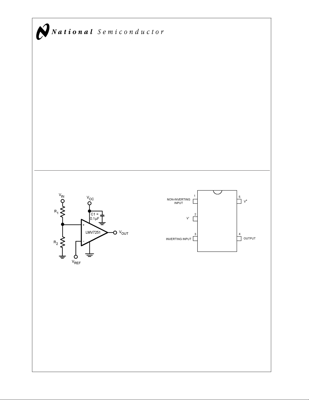
Typical Circuit Connection Diagram
DS200057-1
Top View
DS200057-2
FIGURE 1. Threshold Detector
© 2001 National Semiconductor Corporation DS200057 www.national.com
Page 2
Absolute Maximum Ratings (Note 1)
If Military/Aerospace specified devices are required,
please contact the National Semiconductor Sales Office/
Wave Soldering (10 sec.) 260˚C
Storage Temperature Range −65˚C to +150˚C
Junction Temperature (Note 4) +150˚C
Distributors for availability and specifications.
ESD Tolerance 1KV (Note 2)
LMV7251/LMV7255
V
Differential +/−Supply Voltage
IN
Supply Voltage (V
Voltage at Input/Output pins V
+-V−
) 5.5V
+
+0.1V, V−−0.1V
Soldering Information
Infrared or Convection (20
200V (Note 6)
Operating Ratings (Note 1)
Supply Voltage V
Junction Temperature Range (Note
3) −40˚C to +85˚C
Package Thermal Resisance (Note 3)
SOT23-5 325˚C/W
SC-70 265˚C/W
+
sec.) 235˚C
1.8V Electrical Characteristics
Unless otherwise specified, all limits guaranteed for TJ= 25˚C, V+= 1.8V, V−= 0V. Boldface limits apply at the temperature
extremes.
Symbol Parameter Condition Typ
(Note 4)
V
OS
TC V
I
B
I
OS
I
S
I
SC
Input Offset Voltage 0.3 6
Input Offset Average Drift VCM= 0.9V (Note 7) 10 uV/C
OS
Input Bias Current 14 nA
Input Offset Current 200 pA
Supply Current 11 15
Output Short Circuit Current Sourcing, VO= 0.9V
(LMV7251 only)
= 0.9V 11.6 5
O
300 pA
I
LEAKAGE
Sinking, V
Output Leakage Current VO= 1.8V
(LMV7255 only)
V
OH
Output Voltage High IO= 1.5mA
1.72 1.675 V
(LMV7251 only)
V
OL
V
CM
CMRR Common Mode Rejection Ratio 0
PSRR Power Supply Rejection Ratio V
Output Voltage Low IO= −1.5mA 65 125 mV
Input Common Voltage Range CMRR>45 dB 1.9 V
<
<
V
1.8V 72 47 dB
CM
+
= 1.8V to 5V 79 55 dB
84
Limits
(Note 5)
8
17
−0.1 V
1.8V to 5.0V
Units
mV
max
µA
max
mA
min
min
max
max
min
min
min
1.8V AC Electrical Characteristics
Unless otherwise specified, all limits guaranteed for TJ= 25˚C, V+= 1.8V, V−= 0V, VCM= 0.5V, VO=V+/2. Boldface limits
apply at the temperature extremes.
Symbol Parameter Condition Typ
t
PHL
Propagation Delay
(High to Low)
Input Overdrive = 20mV
Load = 50pF//5kΩ
Input Overdrive = 50mV
Load = 50pF//5kΩ
www.national.com 2
(Note 5)
720 ns
380 ns
Limits
(Note 6)
Units
Page 3
1.8V AC Electrical Characteristics (Continued)
Unless otherwise specified, all limits guaranteed for TJ= 25˚C, V+= 1.8V, V−= 0V, VCM= 0.5V, VO=V+/2. Boldface limits
apply at the temperature extremes.
Symbol Parameter Condition Typ
(Note 5)
t
PLH
Propagation Delay
(Low to High)
Input Overdrive = 20mV
Load = 50pF//5kΩ
Input Overdrive = 50mV
670 ns
400 ns
Limits
(Note 6)
Load = 50pF//5kΩ
2.7V Electrical Characteristics
Unless otherwise specified, all limits guaranteed for TJ= 25˚C, V+= 2.7V, V−= 0V. Boldface limits apply at the temperature
extremes.
Symbol Parameter Conditions Typ
(Note 5)
V
OS
TC V
I
B
I
OS
I
S
I
SC
Input Offset Voltage 0.03 6
Input Offset Average Drift VCM= 1.35V (Note 7) 10 µV/C
OS
Input Bias Current 15 nA
Input offset Current 210 pA
Supply Current 11 18
Output Short Circuit Current Sourcing, VO= 1.35V
(LMV7251 only)
I
LEAKAGE
Sinking, V
Output Leakage Current VO= 2.7V,
= 1.35V 28 15
O
320 pA
(LMV7255 only)
V
OH
Output Voltage High IO= 2mA
2.63 2.575 V
(LMV7251 only)
V
OL
V
CM
CMRR Common Mode Rejection Ratio 0
PSRR Power Supply Rejection Ratio V
Output Voltage Low IO= −2mA 61 125 mV
Input Common Voltage Range CMRR>45dB 2.8 V
<
<
V
2.7V 75 46 dB
CM
+
= 1.8V to 5V 79 55 dB
28 15
Limits
(Note 6)
8
22
−0.1 V
LMV7251/LMV7255
Units
Units
mV
max
µA
max
mA
min
max
max
min
min
min
2.7V AC Electrical Characteristics
Unless otherwise specified, all limits guaranteed for TJ= 25˚C, V+= 2.7V, V−= 0V.Boldface limits apply at the temperature
extremes.
Symbol Parameter Condition Typ
(Note 5)
t
PHL
Propagation Delay
(High to Low)
Input Overdrive = 20mV
Load = 50pF//5kΩ
Input Overdrive = 50mV
830 ns
430 ns
Load = 50pF//5kΩ
t
PLH
Propagation Delay
(Low to High)
Input Overdrive = 20mV
Load = 50pF//5kΩ
Input Overdrive = 50mV
730 ns
410 ns
Load = 50pF//5kΩ
Limits
(Note 6)
www.national.com3
Units
Page 4
5V Electrical Characteristics
Unless otherwise specified, all limits guaranteed for TJ= 25˚C, V+= 5V, V−= 0V. Boldface limits apply at the temperature extremes.
Symbol Parameter Conditions Typ
(Note 5)
V
OS
Input Offset Voltage 0.03 6
LMV7251/LMV7255
TC V
I
B
I
OS
I
S
I
SC
I
LEAKAGE
V
OH
V
OL
Note 1: Absolute Maximum Ratings indicate limits beyond which damage to the device may occur. Operating Ratings indicate conditions for which the device is
intended to be functional, but specific performance is not guaranteed. For guaranteed specifications and the test conditions, see the Electrical Characteristics.
Note 2: Human body model, 1.5kΩ in series with 100pF.
Note 3: The maximum power dissipation is a function of T
=(T
P
D
Note 4: Typical values represent the most likely parametric norm.
Note 5: All limits are guaranteed by testing or statistical analysis.
Note 6: Machine Model, 0Ω in series with 200pF.
Note 7: Offset Voltage average drift determined by dividing the change in V
Input Offset Average Drift VCM= 2.5V (Note 7) 10 µV/C
OS
Input Bias Current 16 nA
Input Offset Current 220 pA
Supply Current 12 20
Output Short Circuit Current Sourcing, VO= 2.5V
82 50
(LMV7251 only)
Sinking, V
Output Leakage Current VO= 5V,
= 2.5V 78 50
O
375 pA
(LMV7255 only)
Output Voltage High IO= 4mA 4.9 4.82 V
Output Voltage Low IO= −4mA 90 180 mV
, θJA, and TA. The maximum allowable power dissipation at any ambient temperature is
J(max)-TA
)/θJA. All numbers apply for packages soldered directly into a PC board.
J(max)
at temperature extremes into the total temperature change.
OS
Limits
(Note 6)
8
25
Units
mV
max
µA
max
mA
min
min
max
www.national.com 4
Page 5
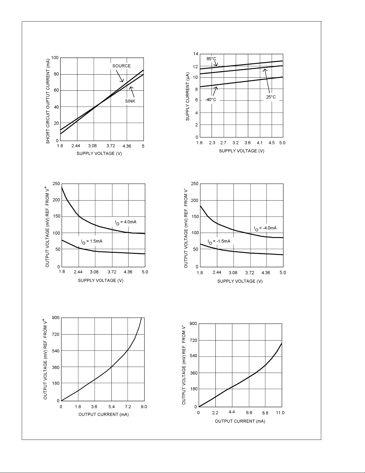
LMV7251/LMV7255
Typical Performance Characteristics (T
Short Circuit Current vs. Supply Voltage
DS200057-3
Output Voltage vs. Supply Voltage
= 25˚C, Unless otherwise specified).
A
Supply Current vs. Supply Voltage
Output Voltage vs. Supply Voltage
DS200057-4
DS200057-5
Output Voltage vs. Output Current@1.8V Supply
Voltage
DS200057-7
DS200057-6
Output Voltage vs. Output Current@1.8V Supply
Voltage
DS200057-8
www.national.com5
Page 6

Typical Performance Characteristics (T
= 25˚C, Unless otherwise specified). (Continued)
A
Output Voltage vs. Output Current
Voltage
LMV7251/LMV7255
Response Time for Various Input Overdrives - t
@
2.7V Supply
DS200057-9
PLH
Output Voltage vs. Output Current@2.7V Supply
Voltage
DS200057-10
Response Time for Various Input Overdrives - t
PHL
DS200057-11
Response Time for Various Input Overdrives - t
PLH
DS200057-13
www.national.com 6
DS200057-12
Response Time for Various Input Overdrives - t
DS200057-14
PHL
Page 7

Application Info
Basic Comparators
A comparator is quite often used to convert an analog signal
to a digital signal. The comparator compares an input voltage (V
(V
(V
output voltage (V
) at the non-inverting pin to the reference voltage
IN
) at the inverting pin. If VINis less than V
REF
) is low (VOL). However, if VINis greater than V
O
) is high (VOH).
O
REF
LMV7251
DS200057-15
LMV7255
the output
, the
REF
hysteresis causes one input to effectively move quickly pass
the other. Thus, effectively moving the input out of region that
oscillation may occur.
Hysteresis can easily be added to a comparator in a
non-inverting configuration with two resistors and positive
feedback
when V
The output will switch from high to low when V
where V
The Hysteresis is the difference between V
∆V
R2)-V
Figure 3
rises up to V
IN
V
=(V
IN1
IN2
V
IN2
IN=VIN1-VIN2
CC
REF
is calculated by
=(V
REF
R1) / R2) = VCCR1/ R2.
. The output will switch from low to high
, where V
IN1
is calculated by
IN1
(R1 + R2))/ R2
falls to V
IN
IN2
(R1+R2)-VCCR1)/R2
= ((V
(R1 + R2)) / R2) - ((V
REF
IN1
and V
REF
.
IN2
(R1 +
LMV7251/LMV7255
,
DS200057-16
Input/Output
DS200057-17
FIGURE 2. Basic Comparator
Hysteresis
The basic comparator configuration may oscillate or produce
a noisy output if the applied differential input is near the
comparator’s input offset voltage. This tends to occur when
the voltage on the input is equal or very close to the other
input voltage. Adding hysteresis can prevent this problem.
Hysteresis creates two switching thresholds (one for the
rising input voltage and the other for the falling input voltage). Hysteresis is the voltage difference between the two
switching thresholds. When both inputs are nearly equal,
DS200057-18
DS200057-19
FIGURE 3. Non-Inverting Comparator Configuration —
LMV7251
For an inverting configured comparator, hysteresis can be
added with a three resistor network and positive feedback.
When input voltage (V
non-inverting node (V
) at the inverting node is less than
IN
), the output is high. The equivalent
T
circuit for the three resistor network is R1 in parallel with R3
and in series with R2. The lower threshold voltage V
T1
calculated by:
V
= ((VCCR2) / ((R1 R3) / (R1+ R3)) + R2)
T1
When V
is greater than VT, the output voltage is low. The
IN
equivalent circuit for the three resistor network is R2 in
parallel with R3 and in series with R1. The upper threshold
voltage V
V
T2=VCC
is calculated by:
T2
((R2 R3) / (R2 + R3)) / ((R1 + ((R2 R3) / (R2 +
R3))
The hysteresis is defined as
∆V
IN=VT1-VT2
(V
((R2 R3) / (R2 + R3)) / ((R1 + ((R2 R3) / (R2 + R3)))
CC
= ((VCCR2) / ((R1 R3) / (R1+ R3)) + R2) –
is
www.national.com7
Page 8

Application Info (Continued)
LMV7251/LMV7255
DS200057-20
Power supply decoupling is critical and improves stability.
Place decoupling capacitors 0.1µF as close as possible to
+
the V
pin. For split supply applications, place decoupling
capacitors 0.1µF on both the V
+
and V−pins. The decoupling
capacitors will help keep the comparator from oscillating
under various load conditions.
DS200057-21
FIGURE 4. Inverting Configured Comparator —
LMV7255
Input Stage
The LMV7251 and LMV7255 have rail-to-rail input stages.
The input common mode voltage range is from −100mV to
(V
+ 100mV).
CC
Output Stage
The LMV7251 has a push-pull CMOS output stage. Large
push-pull output drivers allows rail-to-rail output swings with
load currents in the miliampere range.
The LMV7255 has a open drain CMOS output stage. This
requires an external pull-up resistor connected between the
positive supply voltage and the output. The external pull-up
resistor should be high enough resistance so to avoid excessive power dissipation. In addition, the pull-up resistor
should be low enough resistance to enable the comparator
to switch with the load circuitry connected.
Power Supply Considerations
The LMV7251/LMV7255 are well suited for many batterypowered applications. The LMV7251/LMV7255 can operate
from single power supply of +1.8V to +5V. The device typically consumes only 11µA with a 2.7V supply. With a high
power supply rejection ratio (PSRR) of 79 dB (typical), the
comparator is well suited for operating under conditions of a
decaying battery voltage.
www.national.com 8
Page 9

Ordering Information
Package Ordering Info Pkg Marking Supplied As NSC Drawing
5-Pin SOT23-5 LMV7251M5 C16A 1k Units Tape and Reel MF05A
LMV7251M5X C16A 3k units Tape and Reel
LMV7255M5 C18A 1k Units Tape and Reel
LMV7255M5X C18A 3k units Tape and Reel
5-Pin SC-70 LMV7251M7 C17 1k Units Tape and Reel MAA05A
LMV7251M7X C17 3k units Tape and Reel
LMV7255M7 C19 1k Units Tape and Reel
LMV7255M7X C19 3k units Tape and Reel
LMV7251/LMV7255
www.national.com9
Page 10

Physical Dimensions inches (millimeters) unless otherwise noted
LMV7251/LMV7255
5-Pin SC70-5
NS Package Number MAA05A
www.national.com 10
Page 11

Physical Dimensions inches (millimeters) unless otherwise noted
LMV7251/LMV7255 1.8V Low Voltage Comparator with Rail-to-Rail Input
5-Pin SOT23-5
NS Package Number MF05A
LIFE SUPPORT POLICY
NATIONAL’S PRODUCTS ARE NOT AUTHORIZED FOR USE AS CRITICAL COMPONENTS IN LIFE SUPPORT
DEVICES OR SYSTEMS WITHOUT THE EXPRESS WRITTEN APPROVAL OF THE PRESIDENT AND GENERAL
COUNSEL OF NATIONAL SEMICONDUCTOR CORPORATION. As used herein:
1. Life support devices or systems are devices or
systems which, (a) are intended for surgical implant
into the body, or (b) support or sustain life, and
whose failure to perform when properly used in
accordance with instructions for use provided in the
2. A critical component is any component of a life
support device or system whose failure to perform
can be reasonably expected to cause the failure of
the life support device or system, or to affect its
safety or effectiveness.
labeling, can be reasonably expected to result in a
significant injury to the user.
National Semiconductor
Corporation
Americas
Tel: 1-800-272-9959
Fax: 1-800-737-7018
Email: support@nsc.com
www.national.com
National Semiconductor
Europe
Fax: +49 (0) 180-530 85 86
Email: europe.support@nsc.com
Deutsch Tel: +49 (0) 69 9508 6208
English Tel: +44 (0) 870 24 0 2171
Français Tel: +33 (0) 1 41 91 8790
National Semiconductor
Asia Pacific Customer
Response Group
Tel: 65-2544466
Fax: 65-2504466
Email: ap.support@nsc.com
National Semiconductor
Japan Ltd.
Tel: 81-3-5639-7560
Fax: 81-3-5639-7507
National does not assume any responsibility for use of any circuitry described, no circuit patent licenses are implied and National reserves the right at any time without notice to change said circuitry and specifications.
 Loading...