

Page 1
LMV7235/LMV7239
45ns, Ultra Low Power, Low Voltage, Rail-to-Rail Input
Comparator with Open-Drain/Push-Pull Output
General Description
The LMV7235/39 are ultra low power, low voltage, 45ns
comparators. They are guaranteed to operate over the full
supply voltage range of 2.7V to 5V. These devices achieve a
45ns propagation delay while consuming only 65µA of supply current at 5V.
The LMV7235/39 have a greater than rail-to-rail common
mode voltage range. Theinputcommonmodevoltagerange
extends 200mV below ground and 200mV above supply,
allowing both ground and supply sensing.
The LMV7235 features an open drain output. By connecting
an external resistor, the output of the comparator can be
used as a level shifter.
The LMV7239 features a push-pull output stage. This feature
allows operation without the need of an external pull-up
resistor.
The LMV7235/39 are available in the SC70-5 and SOT23-5
packages, which are ideal for systems where small size and
low power is critical.
Features
(VS=5V,TA= 25˚C, Typical values unless otherwise specified)
n Propagation delay 45ns
n Low supply current 65µA
n Rail-to-Rail input
n Open drain and push-pull output
n Ideal for 2.7V and 5V single supply applications
n Available in space saving packages: 5-pin SOT23-5
and 5-pin SC70-5
Applications
n Portable and battery powered systems
n Scanners
n Set top boxes
n High speed differential line receiver
n Window comparators
n Zero-crossing detectors
n High speed sampling circuits
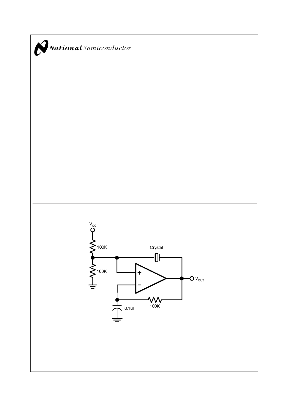
Typical Application
10135902
February 2002
LMV7235/LMV7239 45 nsec, Ultra Low Power, Low Voltage, Rail-to-Rail Input Comparator with
Open-Drain/Push-Pull Output
© 2002 National Semiconductor Corporation DS101359 www.national.com
Page 2
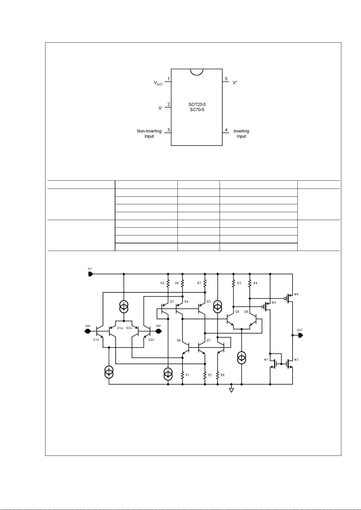
Connection Diagram
SC70-5/SOT23-5
10135903
Top View
Ordering Information
Package Part Number Marking Supplied as NSC Drawing
5-pin SC70-5
LMV7235M7 C21 1k Units Tape and Reel
MAA05ALMV7235M7X C21 3k Units Tape and Reel
LMV7239M7 C20 1k Units Tape and Reel
LMV7239M7X C20 3k Units Tape and Reel
5-pin SOT23-5
LMV7235M5 C21A 1k Units Tape and Reel
MF05ALMV7235M5X C21A 3k Units Tape and Reel
LMV7239M5 C20A 1k Units Tape and Reel
LMV7239M5X C20A 3k Units Tape and Reel
Simplified Schematic
10135901
LMV7235/LMV7239
www.national.com 2
Page 3
Absolute Maximum Ratings (Note 1)
If Military/Aerospace specified devices are required,
please contact the National Semiconductor Sales Office/
Distributors for availability and specifications.
ESD Tolerance (Note 2)
Machine Body 100V
Human Model Body 1000V
Differential Input Voltage
±
Supply Voltage
Output Short Circuit Duration (Note 3)
Supply Voltage (V
+-V−
) 5.5V
Soldering Information
Infrared or Convection (20 sec) 235˚C
Wave Soldering (10 sec) 260˚C (lead temp)
Voltage at Input/Output Pins (V
+
) +0.3V
(V
−
) −0.3V
Current at Input Pin (Note 9)
±
10mA
Operating Ratings
Supply Voltages (V+-V−) 2.7V to 5V
Junction Temperature Range
(Note 4)
−40˚C to +85˚C
Storage Temperature Range −65˚C to +150˚C
Package Thermal Resistance
SC70-5 478˚C/W
SOT23-5 265˚C/W
2.7V Electrical Characteristics
Unless otherwise specified, all limits guaranteed for TJ= 25˚C, VCM=V+/2, V+= 2.7V, V−=0V−.Boldface limits apply at the
temperature extremes.
Symbol Parameter Conditions Typ
(Note 5)
Limits
(Note 6)
Units
V
OS
Input Offset Voltage 0.8 6
8
mV
max
I
B
Input Bias Current 30 400
600
nA
max
I
OS
Input Offset Current 5 200
400
nA
max
CMRR Common Mode Rejection Ratio 0V
<
V
CM
<
2.7V
(Note 7)
62 52 dB
min
PSRR Power Supply Rejection Ratio V
+
= 2.7V to 5V 85 65 dB
min
V
CM
Input Common-Mode Voltage Range CMRR>50dB V++0.2 V++0.1
V
+
V
min
−0.2 −0.1
0
V
max
V
O
Output Swing High
(LMV7239 only)
IL= 4mA,
V
ID
= 500mV
V
+
−0.26 V+−0.35 V
min
I
L
= 0.4mA,
V
ID
= 500mV
V
+
−0.02 V
min
Output Swing Low
(LMV7239/LMV7235)
I
L
= −4mA,
V
ID
= −500mV
230 350
450
mV
max
I
L
= −0.4mA,
V
ID
= −500mV
15 mV
max
I
SC
Output Short Circuit Current Sourcing, VO=0V
(LMV7239 only)
(Note 3)
15 mA
Sinking, V
O
= 2.7V
(LMV7235 R
L
= 10k) (Note 3)
20 mA
I
S
Supply Current No load 52 85
100
µA
max
LMV7235/LMV7239
www.national.com3
Page 4
2.7V Electrical Characteristics (Continued)
Unless otherwise specified, all limits guaranteed for TJ= 25˚C, VCM=V+/2, V+= 2.7V, V−=0V−.Boldface limits apply at the
temperature extremes.
Symbol Parameter Conditions Typ
(Note 5)
Limits
(Note 6)
Units
t
PD
Propagation Delay Overdrive = 20mV
(Note 10)
68 ns
Overdrive = 50mV
(Note 10)
63 ns
Overdrive = 100mV
(Note 10)
50 ns
t
SKEW
Propagation Delay Skew
(LMV7239 only)
(Note 8) 5 ns
t
r
Output Rise Time LMV7239
10% to 90%
1.7 ns
LMV7235
10% to 90%
(Note 10)
112 ns
t
f
Output Fall Time 90% to 10% 1.7 ns
I
LEAKAGE
Output Leakage Current
(LMV7235 only)
3nA
5V Electrical Characteristics
Unless otherwise specified, all limits guaranteed for TJ= 25˚C, VCM=V+/2, V+= 5V, V−= 0V. Boldface limits apply at the
temperature extremes.
Symbol Parameter Conditions Typ
(Note 5)
Limits
(Note 6)
Units
V
OS
Input Offset Voltage 1 6
8
mV
max
I
B
Input Bias Current 30 400
600
nA
max
I
OS
Input Offset Current 5 200
400
nA
max
CMRR Common Mode Rejection Ratio 0V
<
V
CM
<
5V 67 52 dB
min
PSRR Power Supply Rejection Ratio V
+
= 2.7V to 5V 85 65 dB
min
V
CM
Input Common-Mode Voltage Range CMRR>50dB V++0.2 V++0.1
V
+
V
min
−0.2 −0.1
0
V
max
V
O
Output Swing High
(LMV7239 only)
IL= 4mA,
V
ID
= 500mV
V
+
−0.15 V+−0.25 V
min
I
L
= 0.4mA,
V
ID
= 500mV
V
+
−0.01 V
min
Output Swing Low
(LMV7239/LMV7235)
I
L
= −4mA,
V
ID
= −500mV
230 350
450
mV
max
I
L
= −0.4mA,
V
ID
= −500mV
10 mV
max
LMV7235/LMV7239
www.national.com 4
Page 5

5V Electrical Characteristics (Continued)
Unless otherwise specified, all limits guaranteed for TJ= 25˚C, VCM=V+/2, V+= 5V, V−= 0V. Boldface limits apply at the
temperature extremes.
Symbol Parameter Conditions Typ
(Note 5)
Limits
(Note 6)
Units
I
SC
Output Short Circuit Current Sourcing, VO=0V
(LMV7239 only)
(Note 3)
55 25
15
mA
min
Sinking, V
O
=5V
(LMV7235 R
L
= 10k)
(Note 3)
60 30
20
mA
min
I
S
Supply Current No load 65 95
110
µA
max
t
PD
Propagation Delay Overdrive = 20mV
(Note 10)
62 ns
max
Overdrive = 50mV
(Note 10)
57 ns
max
Overdrive = 100mV
(Note 10)
45 ns
max
t
SKEW
Propagation Delay Skew
(LMV7239 only)
(Note 8) 5 ns
t
r
Output Rise Time LMV7239
10% to 90%
1.2 ns
LMV7235
10% to 90%
(Note 10)
100 ns
t
f
Output Fall Time 90% to 10% 1.2 ns
I
LEAKAGE
Output Leakeage Current
(LMV7235 only)
3nA
Note 1: Absolute Maximum Ratings indicate limits beyond which damage to the device may occur. Operating Ratings indicate conditions for which the device is
intended to be functional, but specific performance is not guaranteed. For guaranteed specifications and the test conditions, see the Electrical characteristics.
Note 2: Human body model, 1.5kΩ in series with 100pF. Machine model, 200pF.
Note 3: Applies to both single-supply and split-supply operation. Continuous short circuit operation at elevated ambient temperature can result in exceeding the
maximum allowed junction temperature of 150˚C. Output currents in excess of
±
30mA over long term may adversely affect reliability.
Note 4: The maximum power dissipation is a function of T
J(max)
, θJA, and TA. The maximum allowable power dissipation at any ambient temperature is
P
D
=(T
J(max)-TA
)/θJA. All numbers apply for packages soldered directly into a PC board.
Note 5: Typical Values represent the most likely parametric norm.
Note 6: All limits are guaranteed by testing or statistical analysis.
Note 7: CMRR is not linear over the common mode range. Limits are guaranteed over the worst case from 0 to V
CC/2
or V
CC/2
to VCC.
Note 8: Propagation Delay Skew is defined as the absolute value of the difference between t
PDLH
and t
PDHL
.
Note 9: Limiting input pin current is only necessary for input voltages that exceed absolute maximum input voltage ratings.
Note 10: A 10k pull-up resistor was used when measuring the LMV7235. The rise time of the LMV7235 is a function of the R-C time constant.
LMV7235/LMV7239
www.national.com5
Page 6

Typical Performance Characteristics (Unless otherwise specified, V
S
= 5V, CL= 10pF, TA= 25˚C).
Supply Current vs. Supply Voltage Sourcing Current vs. Output Voltage
10135904
10135905
Sourcing Current vs. Output Voltage Sinking Current vs. Output Voltage
10135906
10135907
Sinking Current vs. Output Voltage Input Bias Current vs. Input Voltage
10135908
10135909
LMV7235/LMV7239
www.national.com 6
Page 7

Typical Performance Characteristics (Unless otherwise specified, V
S
= 5V, CL= 10pF, TA=
25˚C). (Continued)
Input Bias Current vs. Input Voltage Propagation Delay vs. Temperature
10135910
10135911
Propagation Delay vs. Capacitive Load Propagation Delay vs. Capacitive Load
10135912 10135913
Propagation Delay vs. Input Overdrive Propagation Delay vs. Input Overdrive
10135914 10135915
LMV7235/LMV7239
www.national.com7
Page 8

Typical Performance Characteristics (Unless otherwise specified, V
S
= 5V, CL= 10pF, TA=
25˚C). (Continued)
Propagation Delay vs. Common Mode Voltage Propagation Delay vs. Common Mode Voltage
10135916 10135917
Application Section
The LMV7235/LMV7239 are single supply comparators with
45ns of propagation delay and only 65µA of supply current.
The LMV7235/LMV7239 are rail-to-rail input and output. The
typical input common mode voltage range of −0.2V below
the ground to 0.2V above the supply. The LMV7235/39 use a
complimentary PNP and NPN input stage in which the PNP
stage senses common mode voltage near V
−
and the NPN
stage senses common mode voltage near V
+
. If either of the
input signals falls below the negative common mode limit,
the parasitic PN junction formed by the substrate and the
base of the PNP will turn on resulting in an increase of input
bias current.
If one of the input goes above the positive common mode
limit, the output will still maintain the correct logic level as
long as the other input stays within the common mode range.
However, the propagation delay will increase. When both
inputs are outside the common mode voltage range, current
saturation occurs in the input stage, and the output becomes
unpredictable.
The propagation delay does not increase significantly with
large differential input voltages. However, large differential
voltages greater than the supply voltage should be avoided
to prevent damage to the input stage.
The LMV7239 has a push-pull output. When the output
switches, there is a direct path between V
CC
and ground,
causing high output sinking or sourcing current during the
transition. After the transition, the output current decreases
and the supply current settles back to about 65µAat 5V,thus
conserving power consumption.
The LMV7235 has an open drain that requires a pull-up
resistor to a positive supply voltage for the output to switch
properly.When the internal output transistor is off, the output
voltage will be pulled up to the external positive voltage.
Comparator with Hysteresis
The basic comparator configuration may oscillate or produce
a noisy output if the applied differential input voltage is near
the comparator’s offset voltage. This usually happens when
the input signal is moving very slowly across the comparator’s switching threshold. This problem can be prevented by
the addition of hysteresis or positive feedback.
Inverting Comparator with Hysteresis
The inverting comparator with hysteresis requires a three
resistor network that is referenced to the supply voltage V
CC
of the comparator. When VINat the inverting input is less
than V
A
, the voltage at the non-inverting node of the com-
parator (V
IN
<
VA), the output voltage is high (for simplicity
assume V
O
switches as high as VCC). The three network
resistors can be represented as R1//R3 in series with R2.
The lower input trip voltage V
A1
is defined as
V
A1=VCC
R2 / ((R1//R3) + R2)
When V
IN
is greater than VA(V
IN
>
VA), the output voltage is
low, very close to ground. In this case the three network
resistors can be presented as R2//R3 in series with R1. The
upper trip voltage V
A2
is defined as
V
A2=VCC
(R2//R3) / ((R1+ (R2//R3)
The total hysteresis provided by the network is defined as
Delta V
A=VA1-VA2
To assure that the comparator will always switch fully to V
CC
and not be pulled down by the load the resistors, values
should be chosen as follow:
R
PULL-UP
<<
R
LOAD
LMV7235/LMV7239
www.national.com 8
Page 9

Application Section (Continued)
Non-Inverting Comparator with Hysteresis
A non inverting comparator with hysteresis requires a two
resistor network, and a voltage reference (V
REF
) at the in-
verting input. When V
IN
is low, the output is also low. For the
output to switch from low to high, V
IN
must rise up to V
IN1
where V
IN1
is calculated by.
V
IN1
= R1*(V
REF
/R2) + V
REF
When VINis high, the output is also high, to make the
comparator switch back to it’s low state, V
IN
must equal V
REF
before VAwill again equal V
REF.VIN
can be calculated by
V
IN2
=(V
REF
(R1+ R2) - VCCR1)/R2
The hysteresis of this circuit is the difference between V
IN1
and V
IN2
.
Delta V
IN=VCC
R1/R2
Circuit Layout and Bypassing
The LMV7235/39 require high speed layout. Follow these
layout guidelines:
1. Use printed circuit board with a good, unbroken lowinductance ground plane.
2. Place a decoupling capacitor (0.1µF ceramic surface
mount capacitor) as close as possible to V
CC
pin.
3. On the inputs and the output, keep lead lengths as short
as possible to avoid unwanted parasitic feedback around the
comparator. Keep inputs away from output.
4. Solder the device directly to the printed circuit board rather
than using a socket.
5. For slow moving input signals, take care to prevent parasitic feedback. A small capacitor (1000pF or less) placed
between the inputs can help eliminate oscillations in the
transition region. This capacitor causes some degradation to
t
PD
when the source impedance is low.
6. The topside ground plane runs between the output and
inputs.
7. Ground trace from the ground pin runs under the device
up to the bypass capacitor, shielding the inputs from the
outputs.
10135919
FIGURE 1.
10135924
10135920
FIGURE 2. Non-Inverting Comparator with Hysteresis
LMV7235/LMV7239
www.national.com9
Page 10

Application Section (Continued)
Zero-Crossing Detector
The inverting input is connected to ground and the noninverting input is connected to 100mVp-p signal. As the
signal at the non-inverting input crosses 0V, the comparator’s output changes state.
Threshold Detector
Instead of tying the inverting input to 0V, the inverting input
can be tied to a reference voltage. The non-inverting input is
connected to the input. As the input passes the V
REF
thresh-
old, the comparator’s output changes state.
Crystal Oscillator
A simple crystal oscillator using the LMV7239 is shown
below. Resistors R1 and R2 set the bias point at the comparator’s non-inverting input. Resistors R3, R4 and C1 sets
the inverting input node at an appropriate DC average level
based on the output. The crystal’s path provides resonant
positive feedback and stable oscillation occurs. The output
duty cycle for this circuit is roughly 50%, but it is affected by
resistor tolerances and to a lesser extent by the comparator
offset.
IR Receiver
The LMV7239 is an ideal candidate to be used as an infrared
receiver. The infrared photo diode creates a current relative
to the amount of infrared light present. The current creates a
voltage across R
D
. When this voltage level cross the voltage
applied by the voltage divider to the inverting input, the
output transitions.
10135918
FIGURE 3. Zero-Crossing Detector
10135921
FIGURE 4. Threshold Detector
10135922
FIGURE 5. Crystal Oscillator
10135923
FIGURE 6. IR Receiver
LMV7235/LMV7239
www.national.com 10
Page 11

Physical Dimensions inches (millimeters) unless otherwise noted
5-Pin SC70-5
NS Package Number MAA05A
LMV7235/LMV7239
www.national.com11
Page 12

Physical Dimensions inches (millimeters) unless otherwise noted (Continued)
5-Pin SOT23-5
NS Package Number MF05A
LIFE SUPPORT POLICY
NATIONAL’S PRODUCTS ARE NOT AUTHORIZED FOR USE AS CRITICAL COMPONENTS IN LIFE SUPPORT
DEVICES OR SYSTEMS WITHOUT THE EXPRESS WRITTEN APPROVAL OF THE PRESIDENT AND GENERAL
COUNSEL OF NATIONAL SEMICONDUCTOR CORPORATION. As used herein:
1. Life support devices or systems are devices or
systems which, (a) are intended for surgical implant
into the body, or (b) support or sustain life, and
whose failure to perform when properly used in
accordance with instructions for use provided in the
labeling, can be reasonably expected to result in a
significant injury to the user.
2. A critical component is any component of a life
support device or system whose failure to perform
can be reasonably expected to cause the failure of
the life support device or system, or to affect its
safety or effectiveness.
National Semiconductor
Corporation
Americas
Email: support@nsc.com
National Semiconductor
Europe
Fax: +49 (0) 180-530 85 86
Email: europe.support@nsc.com
Deutsch Tel: +49 (0) 69 9508 6208
English Tel: +44 (0) 870 24 0 2171
Français Tel: +33 (0) 1 41 91 8790
National Semiconductor
Asia Pacific Customer
Response Group
Tel: 65-2544466
Fax: 65-2504466
Email: ap.support@nsc.com
National Semiconductor
Japan Ltd.
Tel: 81-3-5639-7560
Fax: 81-3-5639-7507
www.national.com
LMV7235/LMV7239 45 nsec, Ultra Low Power, Low Voltage, Rail-to-Rail Input Comparator with
Open-Drain/Push-Pull Output
National does not assume any responsibility for use of any circuitry described, no circuit patent licenses are implied and National reserves the right at any time without notice to change said circuitry and specifications.
 Loading...