

Page 1
LMV721/LMV722
10MHz, Low Noise, Low Voltage, and Low Power
Operational Amplifier
LMV721/LMV722 10MHz, Low Noise, Low Voltage, and Low Power Operational Amplifier
April 2002
General Description
The LMV721 (Single) and LMV722 (Dual) are low noise, low
voltage, and low power op amps, that can be designed into
a wide range of applications. The LMV721/LMV722 has a
unity gain bandwidth of 10MHz, a slew rate of 5V/us, and a
quiescent current of 930uA/amplifier at 2.2V.
The LMV721/722 are designed to provide optimal performance in low voltage and low noise systems. They provide
rail-to-rail output swing into heavy loads. The input
common-mode voltage range includes ground, and the
maximum input offset voltage are 3.5mV (Over Temp.) for
the LMV721/LMV722. Their capacitive load capability isalso
good at low supply voltages. The operating range is from
2.2V to 5.5V.
The chip is built with National’s advanced Submicron
Silicon-Gate BiCMOS process. The single version, LMV721,
is available in 5 pin SOT23-5 and a SC-70 (new) package.
The dual version, LMV722, is available in a SO-8, MSOP-8
and 8-pin LLP package.
A Battery Powered Microphone Preamplifier
Features
(For Typical, 5 V Supply Values; Unless Otherwise Noted)
n Guaranteed 2.2V and 5.0V Performance
n Low Supply Current LMV721/2 930µA/amplifier
n High Unity-Gain Bandwidth 10MHz
n Rail-to-Rail Output Swing
@
600Ω load 120mV from either rail at 2.2V
@
2kΩ load 50mV from either rail at 2.2V
n Input Common Mode Voltage Range Includes Ground
n Silicon Dust
n Miniature packaging: LLP-8 2.5mm x 3mm x 0.8mm
n Input Voltage Noise
™
, SC70-5 Package 2.0x2.0x1.0 mm
@
2.2V
Applications
n Cellular an Cordless Phones
n Active Filter and Buffers
n Laptops and PDAs
n Battery Powered Electronics
10092244
Silicon Dust™is a trademark of National Semiconductor Corporation.
© 2002 National Semiconductor Corporation DS100922 www.national.com
Page 2
Absolute Maximum Ratings (Note 1)
If Military/Aerospace specified devices are required,
please contact the National Semiconductor Sales Office/
Distributors for availability and specifications.
ESD Tolerance (Note 2)
LMV721/LMV722
Human Body Model 2000V
Machine Model 100V
Differential Input Voltage
Supply Voltage (V
+–V−
) 5.5V
±
Supply Voltage
Soldering Information
Infrared or Convection (20 sec.) 235˚C
Storage Temp. Range −65˚C to 150˚C
Operating Ratings (Note 3)
Supply Voltage 2.2V to 5.0V
Temperature Range −40˚C ≤T
Thermal Resistance (θ
Silicon Dust SC70-5 Pkg 440˚C/W
Tiny SOT23-5 Pkg 265 ˚C/W
SO Pkg, 8-pin Surface Mount 190˚C/W
MSOP Pkg, 8-Pin Mini Surface
Mount
SO Pkg, 14-Pin Surface Mount 145˚C/W
LLP pkg, 8-Pin 58.2˚C/W
)
JA
Junction Temperature (Note 4) 150˚C
2.2V DC Electrical Characteristics
Unless otherwise specified, all limits guaranteed for TJ= 25˚C. V+= 2.2V, V−= 0V, VCM=V+/2, VO=V+/2 and R
Boldface limits apply at the temperature extremes.
Typ
Symbol Parameter Condition
V
OS
TCV
OS
I
B
I
OS
CMRR Common Mode Rejection Ratio 0V ≤ V
PSRR Power Supply Rejection Ratio 2.2V ≤ V
V
CM
Input Offset Voltage 0.02 3
Input Offset Voltage Average Drift 0.6 µV/˚C
Input Bias Current 260 nA
Input Offset Current 25 nA
≤ 1.3V 88 70
CM
+
≤ 5V, VO=0VCM= 0 90 70
Input Common-Mode Voltage
For CMRR ≥ 50dB −0.30 V
Range
A
V
V
O
I
O
I
S
Large Signal Voltage Gain RL=600Ω
= 0.75V to 2.00V
V
O
R
=2kΩ
L
= 0.50V to 2.10V
V
O
Output Swing RL= 600Ω to V+/2 2.125 2.090
R
=2kΩto V+/2 2.177 2.150
L
Output Current Sourcing, VO=0V
(diff) =±0.5V
V
IN
Sinking, V
(diff) =±0.5V
V
IN
= 2.2V
O
Supply Current LMV721 0.93 1.2
LMV722 1.81 2.2
(Note 5)
1.3 V
81 75
84 75
0.071 0.120
0.056 0.080
14.9 10.0
17.6 10.0
≤85˚C
J
235 ˚C/W
>
1MΩ.
L
Limit
(Note 6) Units
mV
3.5
max
dB
64
min
dB
64
min
dB
60
min
dB
60
min
V
2.065
min
V
0.145
max
V
2.125
min
V
0.105
max
mA
5.0
min
mA
5.0
1.5
min
mA
max
2.6
www.national.com 2
Page 3
2.2V AC Electrical Characteristics
Unless otherwise specified, all limits guaranteed for TJ= 25˚C. V+= 2.2V, V−= 0V, VCM=V+/2, VO=V+/2 and R
Boldface limits apply at the temperature extremes.
Symbol Parameter Conditions Typ
(Note 5)
SR Slew Rate (Note 7) 4.9 V/µs
GBW Gain-Bandwidth Product 10 MHz
Φ
m
G
m
e
n
Phase Margin 67.4 Deg
Gain Margin −9.8 dB
Input-Referred Voltage Noise f = 1 kHz 9
L
>
Units
LMV721/LMV722
1MΩ.
i
n
THD Total Harmonic Distortion f = 1 kHz AV=1
Input-Referred Current Noise f = 1 kHz 0.3
= 600Ω,VO= 500 mV
R
L
PP
0.004 %
5V DC Electrical Characteristics
Unless otherwise specified, all limits guaranteed for TJ= 25˚C. V+= 5V, V−= 0V, VCM=V+/2, VO=V+/2 and R
Boldface limits apply at the temperature extremes.
Symbol Parameter Condition
V
OS
TCV
OS
I
B
I
OS
CMRR Common Mode Rejection Ratio 0V ≤ V
PSRR Power Supply Rejection Ratio 2.2V ≤ V
V
CM
Input Offset Voltage −0.08 3
Input Offset Voltage Average Drift 0.6 µV/˚C
Input Bias Current 260 nA
Input Offset Current 25 nA
≤ 4.1V 89 70
CM
+
≤ 5.0V, VO=0VCM= 0 90 70
Input Common-Mode Voltage
For CMRR ≥ 50dB −0.30 V
Range
A
V
V
O
I
O
I
S
Large Signal Voltage Gain RL= 600Ω
= 0.75V to 4.80V
V
O
R
=2kΩ,
L
= 0.70V to 4.90V,
V
O
Output Swing RL= 600Ω to V+/2 4.882 4.840
R
=2kΩto V+/2 4.952 4.930
L
Output Current Sourcing, VO=0V
(diff) =±0.5V
V
IN
Sinking, V
(diff) =±0.5V
V
IN
O
=5V
Supply Current LMV721 1.03 1.4
LMV722 2.01 2.4
Typ
(Note 5)
(Note 6)
4.1 V
87 80
94 85
0.134 0.190
0.076 0.110
52.6 25.0
23.7 15.0
Limit
3.5
64
64
70
70
4.815
0.215
4.905
0.135
12.0
8.5
1.7
2.8
L
>
1MΩ.
Units
mV
max
dB
min
dB
min
dB
min
dB
min
V
min
V
max
V
min
V
max
mA
min
mA
min
mA
max
www.national.com3
Page 4

5V AC Electrical Characteristics
Unless otherwise specified, all limits guaranteed for TJ= 25˚C. V+= 5V, V−= 0V, VCM=V+/2, VO=V+/2 and R
Boldface limits apply at the temperature extremes.
Symbol Parameter Conditions
LMV721/LMV722
SR Slew Rate (Note 7) 5.25 V/µs min
GBW Gain-Bandwidth Product 10.0 MHz
Φ
m
G
m
e
n
Phase Margin 72 Deg
Gain Margin −11 dB
Input-Related Voltage Noise f = 1 kHz 8.5
Typ
(Note 5)
L
>
1MΩ.
Units
i
n
THD Total Harmonic Distortion f = 1kHz, AV=1
Note 1: Absolute Maximum Ratings indicate limits beyond which damage to the device may occur. Operating Ratings indicate conditions for which the device is
intended to be functional, but specific performance is not guaranteed. For guaranteed specifications and the test conditions, see the Electrical Characteristics.
Note 2: Human body model, 1.5 kΩ in series with 100 pF. Machine model, 200Ω in series with 100 pF.
Note 3: Applies to both single-supply and split-supply operation. Continuous short circuit operation at elevated ambient temperature can result in exceeding the
maximum allowed junction temperature of 150˚C. Output currents in excess of 30 mA over long term may adversely affect reliability.
Note 4: The maximum power dissipation is a function of T
=(T
P
D
J(max)–TA
Note 5: Typical Values represent the most likely parametric norm.
Note 6: All limits are guaranteed by testing or statistical analysis.
Note 7: Connected as voltage follower with 1V step input. Number specified is the slower of the positive and negative slew rate.
Input-Referred Current Noise f = 1 kHz 0.2
= 600Ω,VO=1V
R
L
, θJA, and TA. The maximum allowable power dissipation at any ambient temperature is
)/θJA. All numbers apply for packages soldered directly into a PC board.
J(max)
PP
0.001 %
www.national.com 4
Page 5
Typical Performance Characteristics
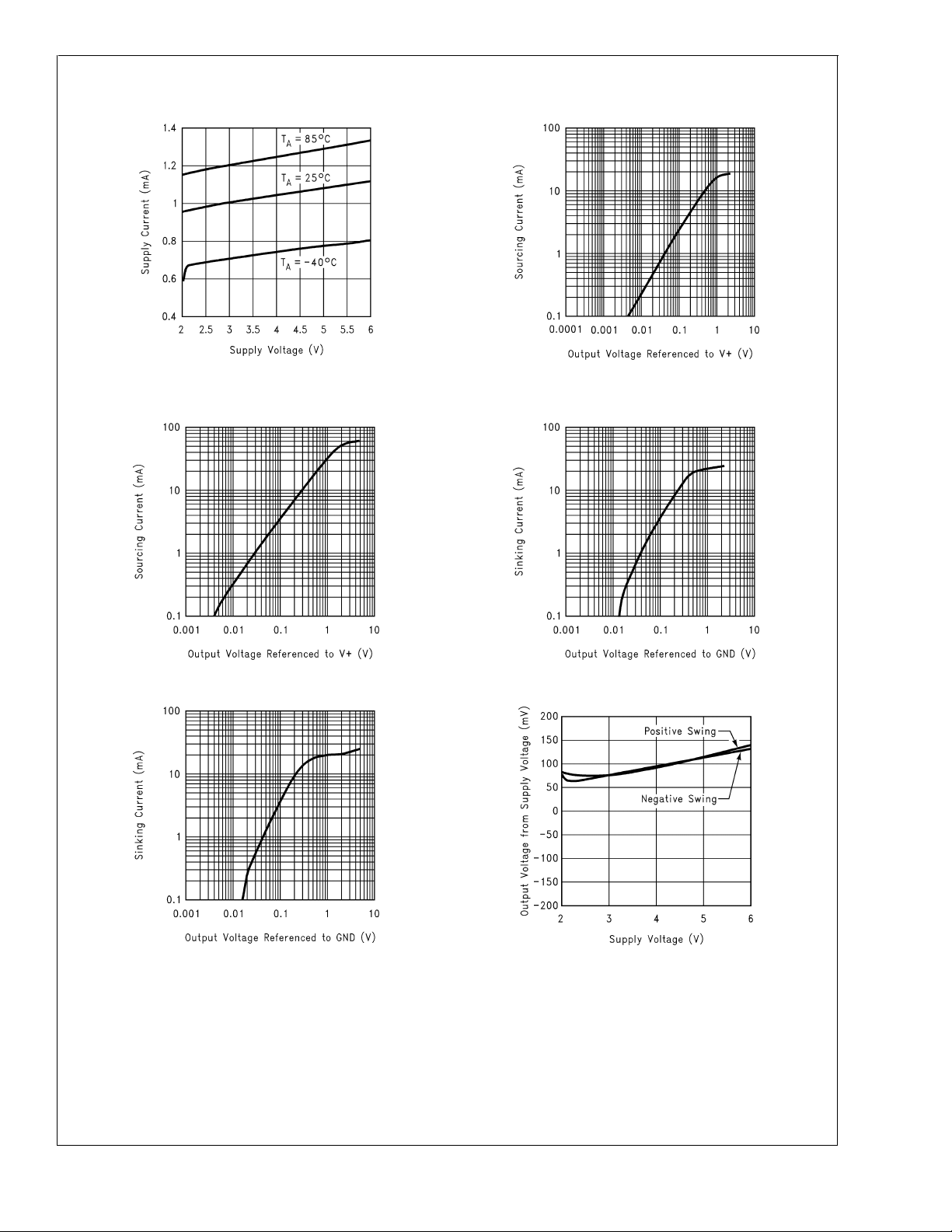
Supply Current vs. Supply Voltage (LMV721) Sourcing Current vs. Output Voltage (VS= 2.2V)
LMV721/LMV722
10092201
10092202
Sourcing Current vs.
Output Voltage (V
= 5V) Sinking Current vs. Output Voltage (VS= 2.2V)
S
10092203 10092204
Sinking Current vs. Output Voltage (VS= 5V) Output Voltage Swing vs. Supply Voltage (RL= 600Ω)
10092205
10092206
www.national.com5
Page 6

Typical Performance Characteristics (Continued)
Output Voltage Swing vs. Suppy Voltage
LMV721/LMV722
Input Offset Voltage vs. Input Common-Mode Voltage
(R
=2kΩ)
L
Range V
S
=5V
10092207
Input Offset Voltage vs. Input Common-Mode Voltage
Range VS= 2.2V
10092208
Input Offset Voltage vs. Supply Voltage
(VCM=V+/2)
10092209
10092210
Input Voltage vs. Output Voltage (VS= 2.2V, RL=2kΩ) Input Voltage vs. Output Voltage (VS= 5V, RL=2kΩ)
10092211 10092212
www.national.com 6
Page 7

Typical Performance Characteristics (Continued)
Input Voltage Noise vs. Frequency Input Current Noise vs. Frequency
10092238 10092232
+PSRR vs. Frequency −PSRR vs. Frequency
LMV721/LMV722
CMRR vs. Frequency
10092213 10092214
Gain and Phase Margin vs. Frequency
(VS= 2.2V, RL600Ω)
10092245 10092215
www.national.com7
Page 8

Typical Performance Characteristics (Continued)
Gain and Phase Margin vs. Frequency
(V
= 5V, RL600Ω) Slew Rate vs. Supply Voltage
S
LMV721/LMV722
THD vs. Frequency
10092216
10092242
10092217
www.national.com 8
Page 9

Application Notes
1.0 Benefits of the LMV721/722 Size.
The small footprints of the LMV721/722 packages save
space on printed circuit boards, and enable the design of
smaller electronic products, such as cellular phones, pagers,
or other portable systems. The low profile of the
LMV721/722 make them possible to use in PCMCIA type III
cards.
Signal Integrity. Signals can pick up noise between the
signal source and the amplifier. By using a physically smaller
amplifier package, the LMV721/722 can be placed closer to
the signal source, reducing noise pickup and increasing
signal integrity.
Simplified Board Layout.These products help you to avoid
using long pc traces in your pc board layout. Thismeans that
no additional components, such as capacitors and resistors,
are needed to filter out the unwanted signals due to the
interference between the long pc traces.
Low Supply Current. These devices will help you to maximize battery life. They are ideal for battery powered systems.
Low Supply Voltage. National provides guaranteed performance at 2.2V and 5V. These guarantees ensure operation
throughout the battery lifetime.
Rail-to-Rail Output. Rail-to-rail output swing provides maximum possible dynamic range at the output. This is particularly important when operating on low supply voltages.
Input Includes Ground. Allows direct sensing near GND in
single supply operation.
Protection should be provided to prevent the input voltages
from going negative more than −0.3V (at 25˚C). An input
clamp diode with a resistor to the IC input terminal can be
used.
2.0 Capacitive Load Tolerance
The LMV721/722 can directly drive 4700pF in unity-gain
without oscillation. The unity-gain follower is the most sensitive configuration to capacitive loading. Direct capacitive
loading reduces the phase margin of amplifiers. The combination of the amplifier’s output impedance and the capacitive
load induces phase lag. This results in either an underdamped pulse response or oscillation. To drive a heavier
capacitive load, circuit in
Figure 1
can be used.
10092231
FIGURE 2. Pulse Response of the LMV721 Circuit in
Figure 1
The circuit in
1
because it provides DC accuracy as well as AC stability. If
Figure 3
there were a load resistor in
voltage divided by R
Figure 3
,RFprovides the DC accuracy by using
feed-forward techniques to connect V
needed in choosing the value of R
current of the LMV721/722. C
is an improvement to the one in
Figure 1
and the load resistor. Instead, in
ISO
F
, the output would be
to RL. Caution is
IN
due to the input bias
F
and R
serve to counteract
ISO
Figure
the loss of phase margin by feeding the high frequency
component of the output signal back to the amplifier’s inverting input, thereby preserving phase margin in the overall
feedback loop. Increased capacitive drive is possible by
increasing the value of C
. This in turn will slow down the
F
pulse response.
10092219
FIGURE 3. Indirectly Driving A Capacitive Load with
DC Accuracy
LMV721/LMV722
10092218
FIGURE 1. Indirectly Driving A capacitive Load Using
Resistive Isolation
In
Figure 1
C
L
, the isolation resistor R
and the load capacitor
ISO
form a pole to increase stability by adding more phase
margin to the overall system. the desired performance depends on the value of R
value, the more stable V
waveform of
C
.
L
Figure 1
. The bigger the R
ISO
will be.
OUT
Figure 2
using 100kΩ for R
ISO
is an output
and 2000µF for
ISO
resistor
3.0 Input Bias Current Cancellation
The LMV721/722 family has a bipolar input stage. The typical input bias current of LMV721/722 is 260nA with 5V
supply.Thus a 100kΩ input resistor will cause 26mV of error
voltage. By balancing the resistor values at both inverting
and non-inverting inputs, the error caused by the amplifier’s
input bias current will be reduced. The circuit in
Figure 4
shows how to cancel the error caused by input bias current.
www.national.com9
Page 10

Application Notes (Continued)
LMV721/LMV722
10092220
FIGURE 4. Cancelling the Error Caused by Input Bias
Current
4.0 Typical Single-Supply Application Circuits
4.1 Difference amplifier
The difference amplifier allows the subtraction of two voltages or, as a special case, the cancellation of a signal
common to two inputs. It is useful as a computational amplifier, in making a differential to single-ended conversion or in
rejecting a common mode signal.
10092221
10092230
FIGURE 6. Three-op-amp Instrumentation Amplifier
The first stage of this instrumentation amplifier is a
differential-input, differential-output amplifier, with two voltage followers. These two voltage followers assure that the
input impedance is over 100MΩ. The gain of this instrumentation amplifier is set by the ratio of R
R
and R4equal R2. Matching of R3to R1and R4to R
1
2/R1.R3
should equal
affects the CMRR. For good CMRR over temperature, low
drift resistors should be used. Making R
than R
between R
and adding a trim pot equal to twice the difference
2
and R4will allow the CMRR to be adjusted for
2
slightly smaller
4
optimum.
4.2.2 Two-op-amp Instrumentation Amplifier
A two-op-amp instrumentation amplifier can also be used to
make a high-input impedance DC differential amplifier (
ure 7
). As in the two-op-amp circuit, this instrumentation
Fig-
amplifier requires precise resistor matching for good CMRR.
R
should equal to R1and R3should equal R2.
4
2
FIGURE 5. Difference Application
4.2 Instrumentation Circuits
The input impendance of the previous difference amplifier is
set by the resistor R
1,R2,R3
and R4. To eliminate the
problems of low input impendance, one way is to use a
voltage follower ahead of each input as shown in the following two instrumentation amplifiers.
4.2.1 Three-op-amp Instrumentation Amplifier
The LMV721/722 can be used to build a three-op-amp instrumentation amplifier as shown in
www.national.com 10
Figure 6
10092222
FIGURE 7. Two-op-amp Instrumentation Amplifier
4.3 Single-Supply Inverting Amplifier
There may be cases where the input signal going into the
amplifier is negative. Because the amplifier is operating in
single supply voltage, a voltage divider using R
and R4is
3
implemented to bias the amplifier so the input signal is within
the input common-common voltage range of the amplifier.
The capacitor C
resistor R
source, V
1
IN
quency, fc =
is placed between the inverting input and
1
to block the DC signal going into the AC signal
. The values of R1and C1affect the cutoff fre-
1
⁄2π R1C1.
Page 11

Application Notes (Continued)
LMV721/LMV722
As a result, the output signal is centered around mid-supply
(if the voltage divider provides V
+
/2 at the non-inverting
input). The output can swing to both rails, maximizing the
signal-to-noise ratio in a low voltage system.
10092223
FIGURE 8. Single-Supply Inverting Amplifier
4.4 Active Filter
4.4.1 Simple Low-Pass Active Filter
The simple low-pass filter is shown in
frequency gain (ω→o) is defined by −R
Figure 9
3/R1
. Its low-pass
. This allows
low-frequency gains other than unity to be obtained. The
filter has a −20dB/decade roll-off after its corner frequency
fc. R
should be chosen equal to the parallel combination of
2
R
and R3to minimize error due to bias current. The fre-
1
quency response of the filter is shown in
Figure 10
.
10092225
FIGURE 10. Frequency Response of Simple Low-pass
Active Filter in
Figure 9
Note that the single-op-amp active filters are used in to the
applications that require low quality factor, Q(≤ 10), low
frequency (≤ 5KHz), and low gain (≤ 10), or a small value for
the product of gain times Q(≤ 100). The op amp should have
an open loop voltage gain at the highest frequency of interest at least 50 times larger than the gain of the filter at this
frequency. In addition, the selected op amp should have a
slew rate that meets the following requirement:
Slew Rate ≥ 0.5x(ω
Where ω
is the highest frequency of interest, and V
H
HVOPP
)X10−6V/µsec
OPP
the output peak-to-peak voltage.
)LEVEL 2
is
10092224
FIGURE 9. Simple Low-Pass Active Filter
10092244
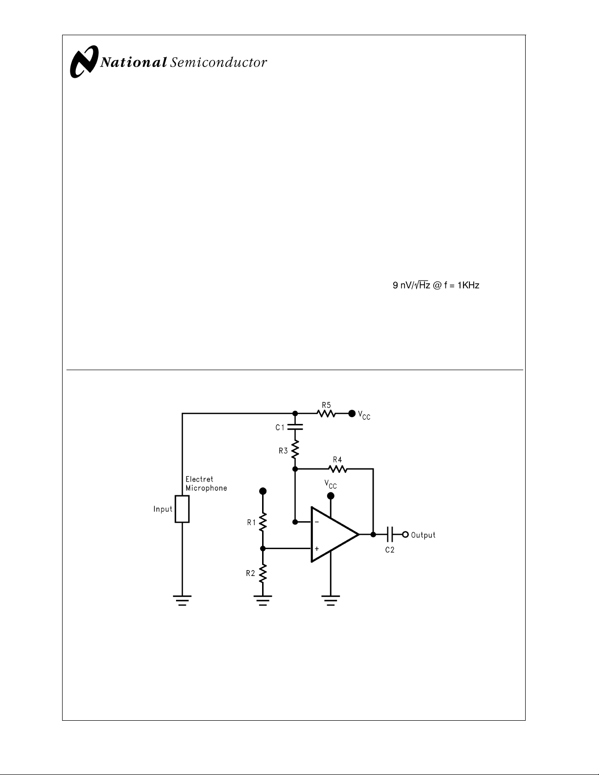
FIGURE 11. A Battery Powered Microphone
Preamplifier
Here is a LMV721 used as a microphone preamplifier. Since
the LMV721 is a low noise and low power op amp, it makes
it an ideal candidate as a battery powered microphone
preamplifier. The LMV721 is connected in an inverting configuration. Resistors, R
half way between V
CC
= 4.7kΩ, sets the reference
1=R2
= 3V and ground. Thus, this configures the op amp for single supply use. The gain of the
preamplifier, which is 50 (34dB), is set by resistors R
10kΩ and R
= 500kΩ. The gain bandwidth product for the
4
3
LMV721 is 10 MHz. This is sufficient for most audio application since the audio range is typically from 20 Hz to 20kHz. A
resistor R
Capacitors C
=5kΩis used to bias the electret microphone.
5
= 4.7µF placed atthe input and output of
1=C2
the op amp to block out the DC voltage offset.
www.national.com11
=
Page 12

Connection Diagrams
5-Pin SC-70/SOT23-5
LMV721/LMV722
Top View
Note: LLP-8 exposed DAP can be electrically connected to ground for improved thermal performance.
10092299
Ordering Information
Temperature Range
Package
8-Pin Small Outline
8-pin MSOP
8-pin LLP
5-Pin SOT23
5-Pin SC-70
−40˚C to +85˚C
LMV722M
LMV722MX 2.5k Units Tape and Reel
LMV722MM
LMV722MMX 3.5k Units Tape and Reel
LMV722LD
LMV722LDX 3.5k Units Tape and Reel
LMV721M5
LMV721M5X 3k Units Tape and Reel
LMV721M7
LMV721M7X 3k Units Tape and Reel
Package Marking Transport Media NSC DrawingIndustrial
LMV722M
LMV722
L22
A30A
A20
8-Pin SO/MSOP/LLP
Top View
Rails
1k Units Tape and Reel
1k Units Tape and Reel
1k Units Tape and Reel
1k Units Tape and Reel
*
10092263
M08A
MUA08A
LDA08C
MF05A
MAA05A
www.national.com 12
Page 13

Physical Dimensions inches (millimeters)
unless otherwise noted
NS Package Number M08A
LMV721/LMV722
8-Pin SOIC
8-Pin LLP
NS Package Number LDA08C
www.national.com13
Page 14

Physical Dimensions inches (millimeters) unless otherwise noted (Continued)
LMV721/LMV722
8-Pin MSOP
NS Package Number MUA08A
www.national.com 14
Page 15

Physical Dimensions inches (millimeters) unless otherwise noted (Continued)
LMV721/LMV722
5-Pin SOT23
NS Package Number MF05A
www.national.com15
Page 16

Physical Dimensions inches (millimeters) unless otherwise noted (Continued)
SC70-5
NS Package Number MAA05A
LIFE SUPPORT POLICY
NATIONAL’S PRODUCTS ARE NOT AUTHORIZED FOR USE AS CRITICAL COMPONENTS IN LIFE SUPPORT
DEVICES OR SYSTEMS WITHOUT THE EXPRESS WRITTEN APPROVAL OF THE PRESIDENT AND GENERAL
COUNSEL OF NATIONAL SEMICONDUCTOR CORPORATION. As used herein:
1. Life support devices or systems are devices or
systems which, (a) are intended for surgical implant
into the body, or (b) support or sustain life, and
whose failure to perform when properly used in
accordance with instructions for use provided in the
2. A critical component is any component of a life
support device or system whose failure to perform
can be reasonably expected to cause the failure of
the life support device or system, or to affect its
safety or effectiveness.
labeling, can be reasonably expected to result in a
LMV721/LMV722 10MHz, Low Noise, Low Voltage, and Low Power Operational Amplifier
significant injury to the user.
National Semiconductor
Corporation
Americas
Email: support@nsc.com
www.national.com
National Semiconductor
Europe
Fax: +49 (0) 180-530 85 86
Email: europe.support@nsc.com
Deutsch Tel: +49 (0) 69 9508 6208
English Tel: +44 (0) 870 24 0 2171
Français Tel: +33 (0) 1 41 91 8790
National Semiconductor
Asia Pacific Customer
Response Group
Tel: 65-2544466
Fax: 65-2504466
Email: ap.support@nsc.com
National Semiconductor
Japan Ltd.
Tel: 81-3-5639-7560
Fax: 81-3-5639-7507
National does not assume any responsibility for use of any circuitry described, no circuit patent licenses are implied and National reserves the right at any time without notice to change said circuitry and specifications.
 Loading...