

Page 1
April 2000
LMV7219
7 nsec, 2.7V to 5V Comparator with Rail-to Rail Output
LMV7219 7 nsec, 2.7V to 5V Comparator with Rail-to Rail Output
General Description
The LMV7219 is a low-power, high-speed comparator with
internal hysteresis. The LMV7219 operating voltage ranges
from 2.7V to 5V with push/pull rail-to-rail output. This device
achieves a 7ns propagation delay while consuming only
1.1mA of supply current at 5V.
The LMV7219 inputs have a common mode voltage range
that extends 200mVbelow ground, allowing ground sensing.
The internal hysteresis ensures clean output transitions even
with slow-moving inputs signals.
The LMV7219 is available in the SC70-5 and SOT23-5 packages, which are ideal for systems where small size and low
power are critical.
Typical Application
Features
(VS=5V,TA= 25˚C, Typical values unless specified)
n Propagation delay 7ns
n Low supply current 1.1mA
n Input common mode voltage range extends 200mv
below ground
n Ideal for 2.7V and 5V single supply applications
n Internal hysteresis ensures clean switching
n Fast rise and fall time 1.3ns
n Available in space-saving packages:
5-pin SC70-5
SOT23-5
Applications
n Portable and battery-powered systems
n Scanners
n Set top boxes
n High speed differential line receiver
n Window comparators
n Zero-crossing detectors
n High-speed sampling circuits
DS101054-1
© 2000 National Semiconductor Corporation DS101054 www.national.com
Page 2
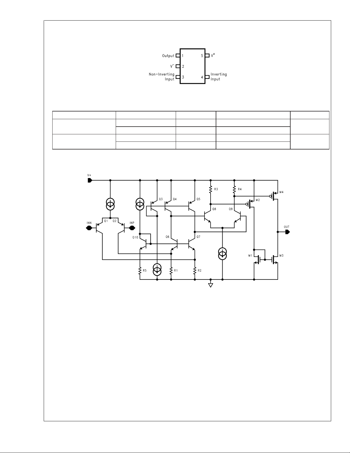
Connection Diagram
LMV7219
Ordering Information
Package Part Number Marking Supplied as NSC Drawing
5-pin SC70-5
5-pin SOT23-5
Simplified Schematic
SC70-5/SOT23-5
DS101054-2
Top View
LMV7219M7 C15 1k Units Tape and Reel
LMV7219M7X C15 3k Units Tape and Reel
LMV7219M5 C14A 1k Units Tape and Reel
LMV7219M5X C14A 3k Units Tape and Reel
MAA05A
MA05B
www.national.com 2
DS101054-3
Page 3

LMV7219
Absolute Maximum Ratings (Note 1)
If Military/Aerospace specified devices are required,
Voltage at Input/Output pins
Current at Input Pin (Note 9)
please contact the National Semiconductor Sales Office/
Distributors for availability and specifications.
ESD Tolerance (Note 2)
Machine Body 150V
Human Model Body 2000V
Differential Input Voltage
±
Supply Voltage
Output Short Circuit Duration (Note 3)
Supply Voltage (V
+-V−
) 5.5V
Soldering Information
Operating Ratings
Supply voltages (V+-V−) 2.7V to 5V
Junction temperature range
(Note 4)
Storage Temperature Range −65˚C to +150˚C
Package Thermal Resistance
SC70-5 478˚C/W
SOT23-5 265˚C/W
−40˚C to +85˚C
Infrared or Convection (20 sec) 235˚C
Wave Soldering (10 sec) 260˚C (lead temp)
2.7V Electrical Characteristics
Unless otherwise specified, all limits guaranteed for TJ= 25˚C, VCM=V+/2, V+= 2.7V, V−= 0V, CL= 10pF and R
−
V
. Boldface limits apply at the temperature extremes.
Symbol Parameter Conditions Typ
(Note 5)
V
OS
I
B
I
OS
CMRR Common Mode Rejection Ratio 0V
PSRR Power Supply Rejection Ratio V
V
CM
Input Offset Voltage 1 6
Input Bias Current 450 950
Input Offset Current 50 200
<
<
V
1.50V 85 62
CM
+
= 2.7V to 5V 85 65
Input Common-Voltage Range CMRR>50dB VCC−1 VCC−1.2
−0.2 −0.1
V
I
I
V
V
V
SC
S
O
HYST
TRIP
TRIP
Output Swing High IL= 4mA,
= 500mV
V
ID
= 0.4mA,
I
L
= 500mV
V
ID
Output Swing Low I
= −4mA,
L
= −500mV
V
ID
= −0.4mA,
I
L
= −500mV
V
ID
Output Short Circuit Current Sourcing,
= 0V (Note 3)
V
O
Sinking,
V
= 2.7V (Note 3)
O
Supply Current No load 0.9 1.6
Input Hysteresis Voltage (Note 10) 7 mV
+
Input Referred Positive Trip Point (see
−
Input Referred Negative Trip Point (see
Figure 1
Figure 1
)38mV
)−4−8mV
V
CC
V
CC
130 200
15 50
20
20
−0.22 VCC−0.3
−0.02 VCC−0.05
Limit
(Note 6)
8
2000
400
55
55
V
CC
0
V
CC
−0.15
V
CC
300
150
2.2
−1.3
−0.4
L
>
1MΩ to
Units
mV
max
nA
max
nA
max
dB
min
dB
min
V
min
V
max
V
min
mV
max
mA
mA
max
max
min
www.national.com3
Page 4
2.7V Electrical Characteristics (Continued)
Unless otherwise specified, all limits guaranteed for TJ= 25˚C, VCM=V+/2, V+= 2.7V, V−= 0V, CL= 10pF and R
LMV7219
V−. Boldface limits apply at the temperature extremes.
Symbol Parameter Conditions Typ
(Note 5)
t
PD
t
SKEW
t
r
t
f
Propagation Delay Overdrive = 5mV
= 0V (Note 7)
V
CM
Overdrive = 15mV
V
= 0V (Note 7)
CM
Overdrive = 50mV
V
= 0V (Note 7)
CM
Propagation Delay Skew (Note 8) 1 ns
Output Rise Time 10% to 90% 2.5 ns
Output Fall Time 90% to 10% 2 ns
12
11
10 20
5V Electrical Characteristics
Unless otherwise specified, all limits guaranteed for TJ= 25˚C, VCM=V+/2, V+= 5V, V−= 0V, CL= 10pF and R
V−. Boldface limits apply at the temperature extremes.
Symbol Parameter Conditions Typ
V
OS
I
B
I
OS
CMRR Common Mode Rejection Ratio 0V
PSRR Power Supply Rejection Ratio V
V
CM
V
O
I
SC
Input Offset Voltage 1 6
Input Bias Current 500 950
Input Offset Current 50 200
<
<
V
3.8V 85 65
CM
+
= 2.7V to 5V 85 65
Input Common-Mode Voltage Range CMRR>50dB VCC−1 VCC−1.2
Output Swing High IL= 4mA,
= 500mV
V
ID
= 0.4mA,
I
L
= 500mV
V
ID
Output Swing Low I
= −4mA,
L
= −500mV
V
ID
= −0.4mA,
I
L
= −500mV
V
ID
Output Short Circuit Current Sourcing, VO=0V
(Note 3)
Sinking, V
O
=5V
(Note 3)
I
V
V
V
S
HYST
Trip
Trip
Supply Current No load 1.1 1.8
Input Hysteresis Voltage (Note 10) 7.5 mV
+
Input Referred Positive Trip Point (See figure 1) 3.5 8 mV
−
Input Referred Negative Trip Point (See figure 1) −4 −8 mV
(Note 5)
−0.2 −0.1
V
−0.13 VCC−0.2
CC
V
−0.02 VCC−0.05
CC
80 180
10 50
68 30
65 30
V
Limit
(Note 6)
Limit
(Note 6)
8
2000
400
55
55
−1.3
V
CC
0
−0.3
V
CC
−0.15
CC
280
150
20
20
2.4
L
>
L
>
1MΩ to
1MΩ to
Units
ns
max
Units
mV
max
nA
max
nA
max
dB
min
dB
min
V
min
V
max
V
min
mV
max
mA
min
mA
max
max
min
www.national.com 4
Page 5

5V Electrical Characteristics (Continued)
Unless otherwise specified, all limits guaranteed for TJ= 25˚C, VCM=V+/2, V+= 5V, V−= 0V, CL= 10pF and R
V−. Boldface limits apply at the temperature extremes.
Symbol Parameter Conditions Typ
(Note 5)
t
PD
Propagation Delay Overdrive = 5mV
= 0V (Note 7)
V
CM
Overdrive = 15mV
V
= 0V (Note 7)
CM
Overdrive = 50mV
V
= 0V (Note 7)
CM
t
SKEW
t
r
t
f
Note 1: Absolute Maximum Ratings indicate limits beyond which damage to the device may occur. Operating Ratings indicate conditions for which the device is intended to be functional, but specific performance is not guaranteed. For guaranteed specifications and the test conditions, see the Electrical characteristics.
Note 2: Human body model, 1.5kΩ in series with 100pF. Machine model, 200Ω in series with 100pF.
Note 3: Applies to both single-supply and split-supply operation. Continuous short circuit operation at elevated ambient temperature can result in exceeding the
maximum allowed junction temperature of 150˚C. Output currents in excess of
Note 4: The maximum power dissipation is a function of T
P
D
Note 5: Typical Values represent the most likely parametric norm.
Note 6: All limits are guaranteed by testing or statistical analysis.
Note 7: Propagation delay measurements made with 100mV steps. Overdrive is measure relative to V
Note 8: Propagation Delay Skew is defined as absolute value of the difference between t
Note 9: Limiting input pin current is only necessary for input voltages that exceed absolute maximum input voltage ratings.
Note 10: The LMV7219 comparator has internal hysteresis. The trip points are the input voltage needed to change the output state in each direction. The offset volt-
age is defined as the average of V
Propagation Delay Skew (Note 8) 0.4 ns
Output Rise Time 10% to 90% 1.3 ns
Output Fall Time 90% to 10% 1.25 ns
±
30mA over long term may adversely affect reliability.
, θJA, and TA. The maximum allowable power dissipation at any ambient temperature is
=(T
J(max)-TA
)/θJA. All numbers apply for packages soldered directly into a PC board.
+
trip
−
and V
, while the hysteresis voltage is the difference of these two.
trip
J(max)
PDLH
and t
PDHL
9
820
719
.
Trip
.
Limit
(Note 6)
L
>
1MΩ to
Units
ns
max
LMV7219
www.national.com5
Page 6

Typical Performance Characteristics Unless otherwise specified, V
=5V,CL= 10pF, TA= 25˚C
S
LMV7219
Supply Current vs.
Supply Voltage
DS101054-4
Input Offset and Trip Voltage vs.
Supply Voltage
VOSvs.
Supply Voltage
DS101054-5
Sourcing Current vs.
Output Voltage
Sourcing Current vs.
Output Voltage
DS101054-6
DS101054-9
DS101054-8
Sinking Current vs.
Output Voltage
DS101054-10
www.national.com 6
Page 7

LMV7219
Typical Performance Characteristics Unless otherwise specified, V
25˚C (Continued)
Sinking Current vs.
Output Voltage
DS101054-11
Propagation Delay vs. Temperature
(V
=5V,Vod= 15mV)
S
Propagation Delay vs. Temperature
(V
= 2.7V, Vod= 15mV)
S
Propagation Delay vs. Capacitive Load
(V
=5V,Vod= 15mV)
S
= 5V, CL= 10pF, TA=
S
DS101054-12
Propagation Delay vs.
Input Overdrive
DS101054-13
DS101054-15
Propagation Delay (t
PD
DS101054-14
−
)
DS101054-16
www.national.com7
Page 8

Typical Performance Characteristics Unless otherwise specified, V
25˚C (Continued)
LMV7219
+
Propagation Delay (t
Application Section
LMV7219 is a single supply comparator with internal hysteresis, 7ns of propagation delay and only 1.1mA of supply current.
The LMV7219 has a typical input common mode voltage
range of −0.2V below the ground to 1V below V
ential input stage is a pair of PNP transistors, therefore, the
input bias current flows out of the device. If either of the input
signals falls below the negative common mode limit, the
parasitic PN junction formed by the substrate and the base
of the PNP will turn on, resulting in an increase of input bias
current.
If one of the inputs goes above the positive common mode
limit, the output will still maintain the correct logic level as
long as the other input stays within the common mode range.
However, the propagation delay will increase. When both inputs are outside the common mode voltage range, current
saturation occurs in the input stage, and the output becomes
unpredictable.
The propagation delay does not increase significantly with
large differential input voltages. However, large differential
voltages greater than the supply voltage should be avoided
to prevent damages to the input stage.
The LMV7219 has a push pull output. When the output
switches, there is a direct path between V
causing high output sinking or sourcing current during the
transition. After the transition, the output current decreases
and the supply current settles back to about 1.1mA at 5V,
thus conserving power consumption.
Most high-speed comparators oscillate when the voltage of
one of the inputs is close to or equal to the voltage on the
other input due to noise or undesirable feedback. The
LMV7219 have 7mV of internal hysteresis to counter parasitic effects and noise. The hysteresis does not change significantly with the supply voltages and the common mode input voltages as reflected in the specification table.
The internal hysteresis creates two trip points, one for the
rising input voltage and one for the falling input voltage. The
difference between the trip points is the hysteresis. With internal hysteresis, when the comparator’s input voltages are
equal, the hysteresis effectively causes one comparatorinput voltage to move quickly past the other, thus taking the
input out of the region where oscillation occurs. Standard
PD
)
DS101054-17
cc
cc
. The differ-
and ground,
comparators require hysteresis to be added with external resistors. The fixed internal hysteresis eliminates these
resistors.
FIGURE 1. Input and Output Waveforms, Non-Inverting
Additional Hysteresis
If additional hysteresis is desired, this can be done with the
addition of three resistors using positive feedback, as shown
in
Figure 2
parator response time. Calculate the resistor values as follows:
1) Select R3. The current through R3 should be greater than
the input bias current to minimize errors. The current through
R3 (I
) at the trip point is (V
F
possible output states when solving for R3, and use the
smaller of the two resulting resistor values. The two formulas
are:
R3=V
REF/IF
R3=V
CC-VREF/IF
2) Choose a hysteresis band required (V
3) Calculate R1, where R1 = R3 X(V
4) Choose the trip point for V
voltage (V
high as V
THR
IN
5) Calculate R2 as follows:
6) Verify the trip voltage and hysteresis as follows:
= 5V, CL= 10pF, TA=
S
DS101054-18
Input Varied
. The positive feedback method slows the com-
REF-VOUT
(when V
(V
) /R3. Consider the two
=0)
OUT
OUT=VCC
IN
)
).
HB
)
HB/VCC
rising. This is the threshold
) at which the comparator switches from low to
rises about the trip point.
www.national.com 8
Page 9

Application Section (Continued)
This method is recommended for additional hysteresis of up
to a few hundred millivolts. Beyond that, the impedance of
R3 is low enough to affect the bias string and adjustment of
R1 may be also required.
DS101054-22
FIGURE 3. Zero-Crossing Detector
Threshold Detector
Instead of tying the inverting input to 0V, the inverting input
can be tied to a reference voltage. The non-inverting input is
connected to the input. As the input passes the V
REF
thresh-
old, the comparator’s output changes state.
LMV7219
DS101054-21
FIGURE 2. Additional Hysteresis
Circuit Layout and Bypassing
The LMV7219 requires high-speed layout. Follow these layout guidelines:
1. Power supply bypassing is critical, and will improve stability and transient response. A decoupling capacitor such as
0.1µF ceramic should be placed as close as possible to V
pin. An additional 2.2µF tantalum capacitor may be required
for extra noise reduction.
2. Keep all leads short to reduce stray capacitance and lead
inductance. It will also minimize unwanted parasitic feedback
around the comparator.
3. The device should be soldered directly to the PC board instead of using a socket.
4. Use a PC board with a good, unbroken low inductance
ground plane. Make sure ground paths are low-impedance,
especially were heavier currents are flowing.
5. Input traces should be kept away from output traces. This
can be achieved by running a topside ground plane between
the output and inputs.
6. Run the ground trace under the device up to the bypass
capacitor to shield the inputs from the outputs.
7. To prevent parasitic feedback when input signals are
slow-moving, a small capacitor of 1000pF or less can be
placed between the inputs. It can also help eliminate oscillations in the transition region. However, this capacitor can
cause some degradation to tpd when the source impedance
is low.
Zero-Crossing Detector
The inverting input is connected to ground and the noninverting input is connected to 100mVp-p signal. As the signal at the non-inverting input crosses 0V, the comparator’s
output Changes State.
DS101054-23
FIGURE 4. Threshold Detector
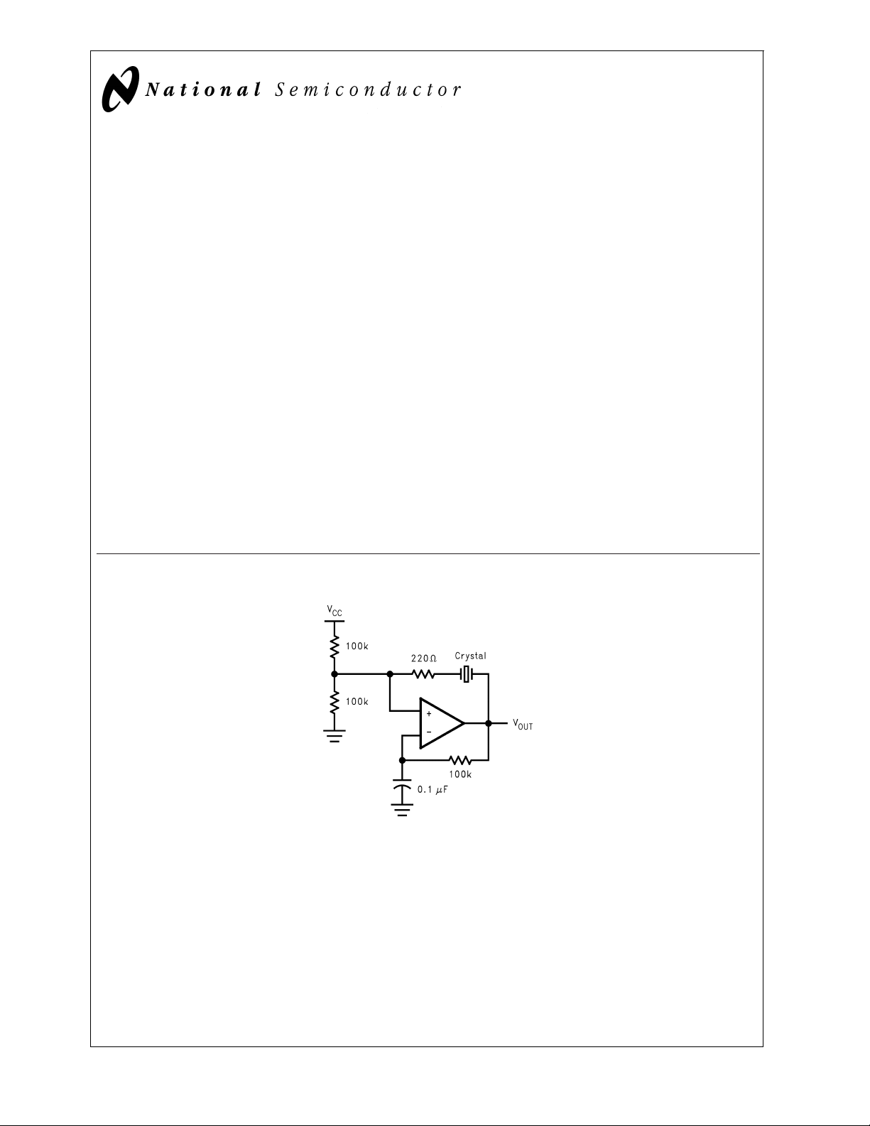
Crystal Oscillator
A simple crystal oscillator using the LMV7219 is shown below. Resistors R1 and R2 set the bias point at the comparator’s non-inverting input. Resistors R3, R4 and C1 sets the
+
inverting input node at an appropriate DC average level
based on the output. The crystal’s path provides resonant
positive feedback and stable oscillation occurs. The output
duty cycle for this circuit is roughly 50%, but it is affected by
resistor tolerances and to a lesser extent by the comparator
offset.
DS101054-24
FIGURE 5. Crystal Oscillator
www.national.com9
Page 10

Application Section (Continued)
IR Receiver
LMV7219
The LMV7219 is an ideal candidate to be used as an infrared
receiver. The infrared photo diode creates a current relative
to the amount of infrared light present. The current creates a
voltage across RD. When this voltage level cross the voltage
applied by the voltage divider to the inverting input, the output transitions.
DS101054-25
FIGURE 6. IR Receiver
www.national.com 10
Page 11

Physical Dimensions inches (millimeters) unless otherwise noted
LMV7219
5-Pin SC70-5 Tape and Reel
Order Numbers LMV7219M7 or LMV7219M7X
NS Package Number MAA05A
www.national.com11
Page 12

Physical Dimensions inches (millimeters) unless otherwise noted (Continued)
5-Pin SOT23-5 Tape and Reel
Order Numbers LMV7219M5 or LMV7219M5X
NS Package Number MA05B
LMV7219 7 nsec, 2.7V to 5V Comparator with Rail-to Rail Output
LIFE SUPPORT POLICY
NATIONAL’S PRODUCTS ARE NOT AUTHORIZED FOR USE AS CRITICAL COMPONENTS IN LIFE SUPPORT
DEVICES OR SYSTEMS WITHOUT THE EXPRESS WRITTEN APPROVAL OF THE PRESIDENT AND GENERAL
COUNSEL OF NATIONAL SEMICONDUCTOR CORPORATION. As used herein:
1. Life support devices or systems are devices or
systems which, (a) are intended for surgical implant
into the body, or (b) support or sustain life, and
whose failure to perform when properly used in
accordance with instructions for use provided in the
labeling, can be reasonably expected to result in a
significant injury to the user.
National Semiconductor
Corporation
Americas
Tel: 1-800-272-9959
Fax: 1-800-737-7018
Email: support@nsc.com
www.national.com
National Semiconductor
Europe
Fax: +49 (0) 180-530 85 86
Email: europe.support@nsc.com
Deutsch Tel: +49 (0) 69 9508 6208
English Tel: +44 (0) 870 24 0 2171
Français Tel: +33 (0) 1 41 91 8790
2. A critical component is any component of a life
support device or system whose failure to perform
can be reasonably expected to cause the failure of
the life support device or system, or to affect its
safety or effectiveness.
National Semiconductor
Asia Pacific Customer
Response Group
Tel: 65-2544466
Fax: 65-2504466
Email: ap.support@nsc.com
National Semiconductor
Japan Ltd.
Tel: 81-3-5639-7560
Fax: 81-3-5639-7507
National does not assume any responsibility for use of any circuitry described, no circuit patent licenses are implied and National reserves the right at any time without notice to change said circuitry and specifications.
 Loading...