

Page 1
January 9, 2009
LMV710/LMV711/LMV715
Low Power, RRIO Operational Amplifiers with High Output
Current Drive and Shutdown Option
LMV710/LMV711/LMV715 Low Power, RRIO Operational Amplifiers with High Output Current
Drive and Shutdown Option
General Description
The LMV710/LMV711/LMV715 are BiCMOS operational amplifiers with a CMOS input stage. These devices have greater
than RR input common mode voltage range, rail-to-rail output
and high output current drive. They offer a bandwidth of 5 MHz
and a slew rate of 5 V/µs.
On the LMV711/LMV715, a separate shutdown pin can be
used to disable the device and reduces the supply current to
0.2 µA (typical). They also feature a turn on time of less than
10 µs. It is an ideal solution for power sensitive applications,
such as cellular phone, pager, palm computer, etc. In addition, once the LMV715 is in shutdown the output will be “Tristated”.
The LMV710 is offered in the space saving 5-Pin SOT23 Tiny
package. The LMV711/LMV715 are offered in the space saving 6-Pin SOT23 Tiny package.
The LMV710/LMV711/LMV715 are designed to meet the demands of low power, low cost, and small size required by
cellular phones and similar battery powered portable electronics.
Typical Application
Features
(For 5V supply, typical unless otherwise noted).
Low offset voltage 3 mV, max
■
Gain-bandwidth product 5 MHz, typ
■
Slew rate 5 V/µs, typ
■
Space saving packages 5-Pin and 6-Pin SOT23
■
Turn on time from shutdown <10 µs
■
Industrial temperature range −40°C to +85°C
■
Supply current in shutdown mode 0.2 µA, typ
■
Guaranteed 2.7V and 5V performance
■
Unity gain stable
■
Rail-to-rail input and output
■
Capable of driving 600Ω load
■
Applications
Wireless phones
■
GSM/TDMA/CDMA power amp control
■
AGC, RF power detector
■
Temperature compensation
■
Wireless LAN
■
Bluetooth
■
HomeRF
■
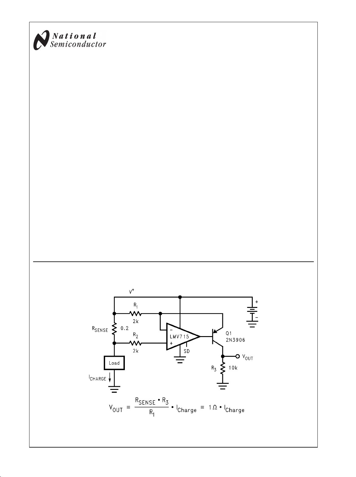
High Side Current Sensing
10132513
© 2009 National Semiconductor Corporation 101325 www.national.com
Page 2
Absolute Maximum Ratings (Note 1)
If Military/Aerospace specified devices are required,
please contact the National Semiconductor Sales Office/
Distributors for availability and specifications.
ESD Tolerance (Note 2)
Machine Model 100V
Human Body Model 2000V
Differential Input Voltage ± Supply Voltage
Voltage at Input/Output Pin (V+) + 0.4V
LMV710/LMV711/LMV715
Supply Voltage (V+ - V −)
Output Short Circuit to V
Output Short Circuit to V
+
−
(V−) − 0.4V
5.5V
(Note 3)
(Note 4)
Current at Input Pin ± 10 mA
Mounting Temp.
Infrared or Convection (20 sec) 235°C
Storage Temperature Range −65°C to 150°C
Junction Temperature (T
JMAX
)
(Note 5)
Operating Ratings (Note 1)
Supply Voltage 2.7V to 5.0V
Temperature Range −40°C to 85°C
Thermal Resistance (θJA)
MF05A Package, 5-Pin SOT23 265 °C/W
MF06A package, 6-Pin SOT23 265 °C/W
2.7V Electrical Characteristics
Unless otherwise specified, all limits guaranteed for TJ = 25°C. V+ = 2.7V, V − = 0V, VCM = 1.35V and RL > 1 MΩ. Boldface limits
apply at the temperature extremes.
Symbol Parameter Condition Typ
(Note 6)
V
OS
I
B
CMRR Common Mode Rejection Ratio
PSRR Power Supply Rejection Ratio
Input Offset Voltage VCM = 0.85V and VCM = 1.85V 0.4 3
Input Bias Current 4 pA
0 ≤ VCM ≤ 2.7V
2.7V ≤ V+ ≤ 5V,
VCM = 0.85V
2.7V ≤ V+ ≤ 5V,
VCM = 1.85V
V
CM
I
SC
Input Common-Mode Voltage Range
For CMRR ≥ 50 dB
Output Short Circuit Current Sourcing
VO = 0V
Sinking
VO = 2.7V
V
O
Output Swing
RL = 10 kΩ to 1.35V
RL = 600Ω to 1.35V
VO (SD) Output Voltage Level in
50 200 mV
Shutdown Mode (LMV711 only)
IO (SD) Output Leakage Current in
1 pA
Shutdown Mode (LMV715 Only)
CO (SD) Output Capacitance in
32 pF
Shutdown Mode (LMV715 Only)
I
S
Supply Current On Mode 1.22 1.7
Shutdown Mode, VSD = 0V 0.002 10 µA
75 50
110 70
95 70
-0.3 -0.2
3 2.9
28 15
40 25
2.68 2.62
0.01 0.12
2.55 2.52
0.05 0.23
Limits
(Note 7)
3.2
45
68
68
12
22
2.60
0.15
2.50
0.30
1.9
150°C
Units
mV
max
dB
min
dB
min
dB
min
V
mA
min
mA
min
V
min
V
max
V
min
V
max
mA
max
www.national.com 2
Page 3
LMV710/LMV711/LMV715
Symbol Parameter Condition Typ
(Note 6)
A
V
Large Signal Voltage Sourcing
RL = 10 kΩ
115 80
Limits
(Note 7)
76
Units
dB
min
VO = 1.35V to 2.3V
Sinking
RL = 10 kΩ
113 80
76
dB
min
VO = 0.4V to 1.35V
Sourcing
RL = 600Ω
110 80
76
dB
min
VO = 1.35V to 2.2V
Sinking
RL = 600Ω
100 80
76
dB
min
VO = 0.5V to 1.35V
SR Slew Rate (Note 8) 5 V/µs
GBWP Gain-Bandwidth Product 5 MHz
φ
m
T
ON
V
SD
Phase Margin 60 Deg
Turn-on Time from Shutdown <10 µs
Shutdown Pin Voltage Range On Mode 1.5 to 2.7 2.4 to 2.7 V
Shutdown Mode 0 to 1 0 to 0.8 V
e
n
Input-Referred Voltage Noise f = 1 kHz 20
3.2V Electrical Characteristics
Unless otherwise specified, all limits guaranteed for TJ = 25°C. V+ = 3.2V, V− = 0V, VCM = 1.6V. Boldface limits apply at the
temperature extremes.
Symbol Parameter Conditions Typ
(Note 6)
V
O
Output Swing IO = 6.5 mA 3.0 2.95
Limit
(Note 7)
2.92
0.01 0.18
0.25
5V Electrical Characteristics
Unless otherwise specified, all limits guaranteed for TJ = 25°C. V+ = 5V, V − = 0V, VCM = 2.5V, and RL > 1 MΩ. Boldface limits
apply at the temperature extremes.
Symbol Parameter Condition Typ
(Note 6)
V
OS
I
B
CMRR Common Mode Rejection Ratio
PSRR Power Supply Rejection Ratio
Input Offset Voltage VCM = 0.85V and VCM = 1.85V 0.4 3
Input Bias Current 4 pA
0V ≤ VCM ≤ 5V
2.7V ≤ V+ ≤ 5V,
VCM = 0.85V
2.7V ≤ V+ ≤ 5V,
VCM = 1.85V
V
CM
Input Common-Mode Voltage Range
For CMRR ≥ 50 dB
70 50
110 70
95 70
-0.3 −0.2
5.3 5.2
Limits
(Note 7)
3.2
48
68
68
Units
V
min
V
max
Units
mV
max
dB
min
dB
min
dB
min
V
3 www.national.com
Page 4
Symbol Parameter Condition Typ
(Note 6)
I
SC
Output Short Circuit Current Sourcing
VO = 0V
Sinking
VO = 5V
V
O
Output Swing
RL = 10 kΩ to 2.5V
35 25
40 25
4.98 4.92
Limits
(Note 7)
21
21
4.90
0.01 0.12
LMV710/LMV711/LMV715
RL = 600Ω to 2.5V
4.85 4.82
0.15
4.80
0.05 0.23
0.3
VO (SD) Output Voltage Level in
50 200 mV
Shutdown Mode (LMV711 only)
IO (SD) Output Leakage Current in
1 pA
Shutdown Mode (LMV715 Only)
CO (SD) Output Capacitance in
32 pF
shutdown Mode (LMV715 Only)
I
S
Supply Current On Mode 1.17 1.7
1.9
Shutdown Mode 0.2 10 µA
A
V
Large Signal Voltage Gain Sourcing
RL = 10 kΩ
123 80
76
VO = 2.5V to 4.6V
Sinking
RL = 10 kΩ
120 80
76
VO = 0.4V to 2.5V
Sourcing
RL = 600Ω
110 80
76
VO = 2.5V to 4.5V
Sinking
RL = 600Ω
118 80
76
VO = 0.5V to 2.5V
SR Slew Rate (Note 8) 5 V/µs
GBWP Gain-Bandwidth Product 5 MHz
φ
m
T
ON
V
SD
Phase Margin 60 Deg
Turn-on Time from Shutdown <10 µs
Shutdown Pin Voltage Range On Mode 2 to 5 2.4 to 5
Shutdown Mode 0 to 1.5 0 to 0.8
e
n
Input-Referred Voltage Noise f = 1 kHz 20
Units
mA
min
mA
min
V
min
V
max
V
min
V
max
mA
max
dB
min
dB
min
dB
min
dB
min
V
Note 1: Absolute Maximum Ratings indicate limits beyond which damage to the device may occur. Operating Ratings indicate conditions for which the device is
intended to be functional, but specific performance is not guaranteed. For guaranteed specifications and the test conditions, see the Electrical Characteristics.
Note 2: Human body model, 1.5 kΩ in series with 100 pF. Machine model, 0Ω in series with 100 pF.
Note 3: Shorting circuit output to V+ will adversely affect reliability.
Note 4: Shorting circuit output to V− will adversely affect reliability.
Note 5: The maximum power dissipation is a function of T
PD = (T
Note 6: Typical values represent the most likely parametric norm.
Note 7: All limits are guaranteed by testing or statistical analysis.
Note 8: Number specified is the slower of the positive and negative slew rates.
www.national.com 4
- T A)/θJA. All numbers apply for packages soldered directly into a PC board.
J(MAX)
, θJA, and TA. The maximum allowable power dissipation at any ambient temperature is
J(MAX)
Page 5
LMV710/LMV711/LMV715
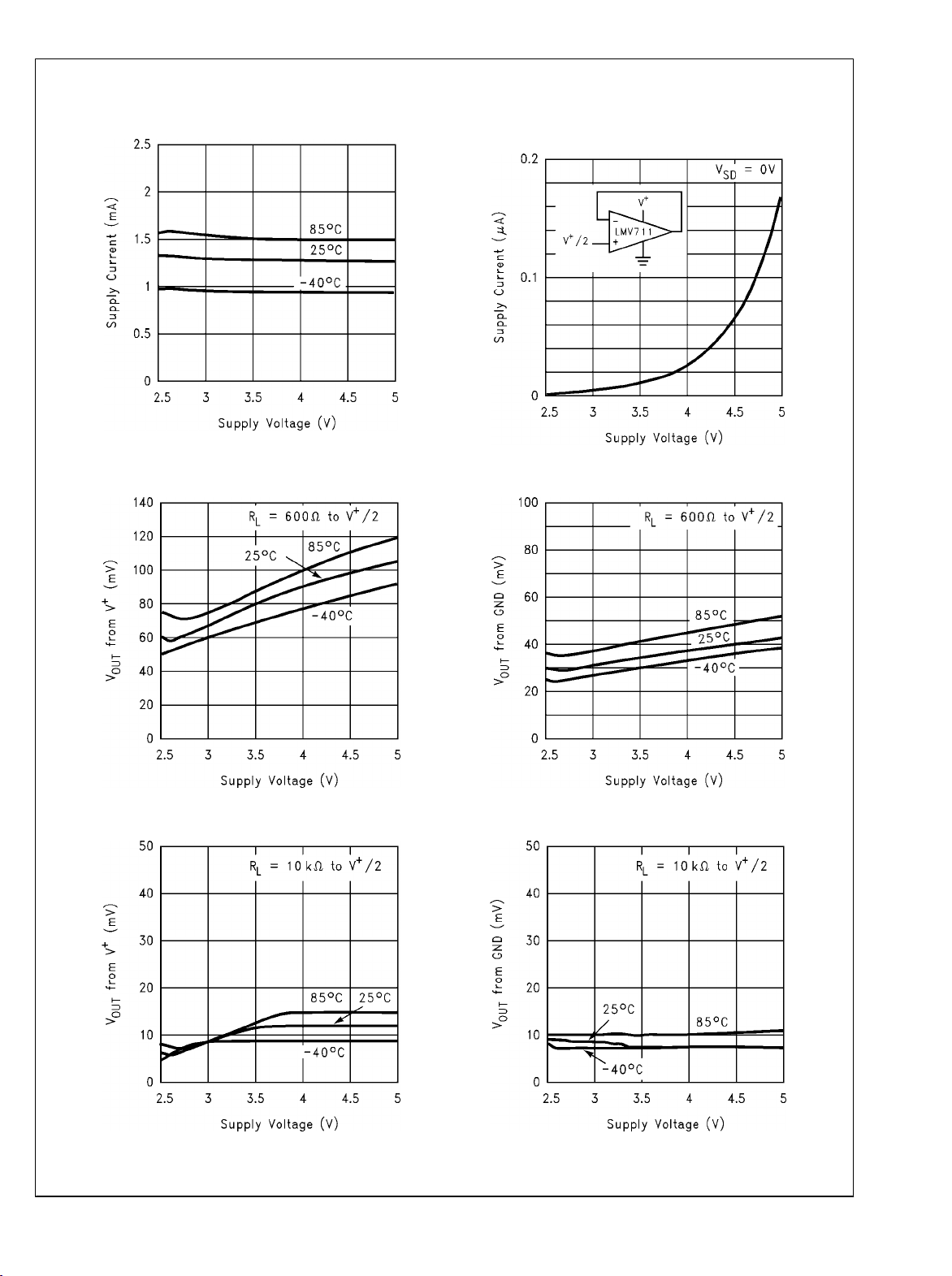
Typical Performance Characteristics Unless otherwise specified, V
Supply Current vs. Supply Voltage (On Mode)
10132527
Output Positive Swing vs. Supply Voltage
LMV711/LMV715 Supply Current vs.
Supply Voltage (Shutdown Mode)
Output Negative Swing vs. Supply Voltage
= +5V, single supply, TA = 25°C.
S
10132528
10132529
Output Positive Swing vs. Supply Voltage
10132531
10132530
Output Negative Swing vs. Supply Voltage
10132532
5 www.national.com
Page 6
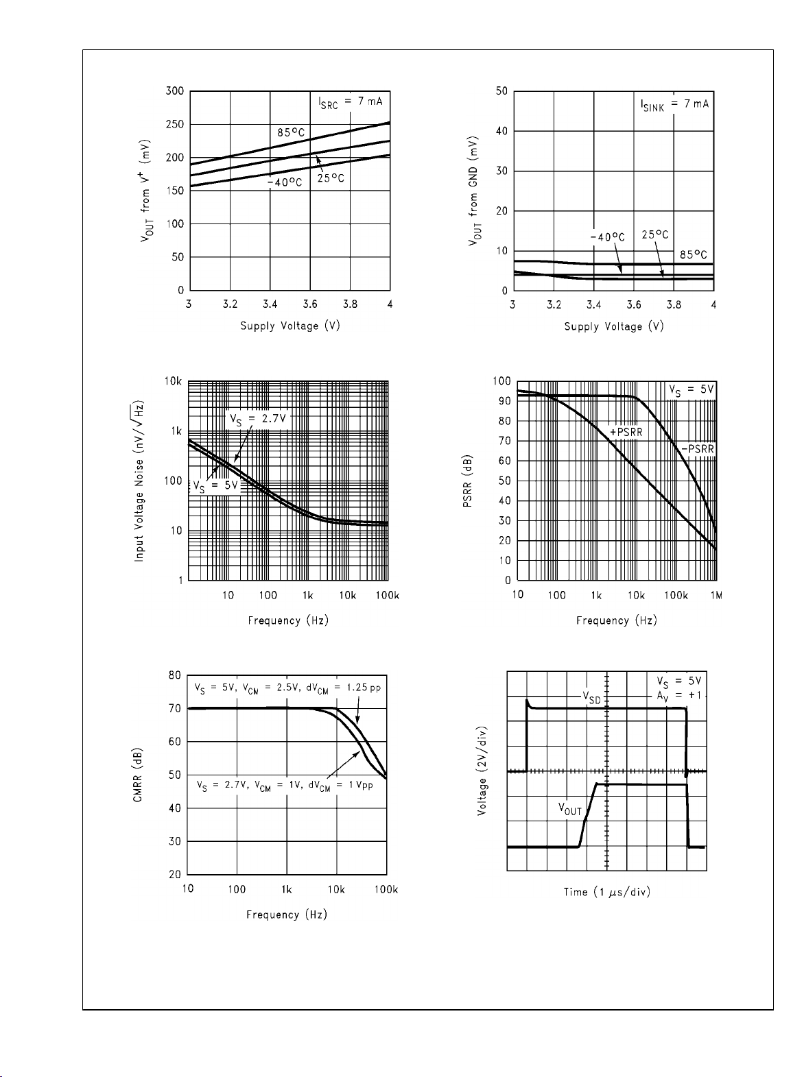
Output Positive Swing vs. Supply Voltage
LMV710/LMV711/LMV715
Output Negative Swing vs. Supply Voltage
Input Voltage Noise vs. Frequency
CMRR vs. Frequency
10132533
10132535
10132534
PSRR vs. Frequency
10132536
LMV711/LMV715 Turn On Characteristics
10132537
www.national.com 6
10132538
Page 7

LMV710/LMV711/LMV715
Sourcing Current vs. Output Voltage
THD+N vs. Frequency (VS = 5V)
10132539
Sinking Current vs. Output Voltage
10132540
THD+N vs. Frequency (VS = 2.7V)
THD+N vs. V
OUT
10132541
10132543
10132542
THD+N vs. V
OUT
10132544
7 www.national.com
Page 8

CCM vs. V
LMV710/LMV711/LMV715
CM
CCM vs. V
CM
C
vs. VCM (VS = 2.7V)
DIFF
Open Loop Frequency Response
10132545
10132547
C
vs. VCM (VS = 5V)
DIFF
Open Loop Frequency Response
10132546
10132548
10132512
www.national.com 8
10132510
Page 9

LMV710/LMV711/LMV715
Open Loop Frequency Response
Open Loop Frequency Response
10132511
Open Loop Frequency Response
10132507
Open Loop Frequency Response
Non-Inverting Large Signal Pulse Response
10132503
10132509
Non-Inverting Small Signal Pulse Response
9 www.national.com
10132508
10132502
Page 10

Inverting Large Signal Pulse Response
LMV710/LMV711/LMV715
Inverting Small Signal Pulse Response
VOS vs. V
CM
10132504
10132549
VOS vs. V
10132505
CM
10132550
www.national.com 10
Page 11

Application Information
1.0 SUPPLY BYPASSING
The application circuits in this datasheet do not show the
power supply connections and the associated bypass capacitors for simplification. When the circuits are built, it is always
required to have bypass capacitors. Ceramic disc capacitors
(0.1 µF) or solid tantalum (1 µF) with short leads, and located
close to the IC are usually necessary to prevent interstage
coupling through the power supply internal impedance. Inadequate bypassing will manifest itself by a low frequency oscillation or by high frequency instabilities. Sometimes, a 10 µF
(or larger) capacitor is used to absorb low frequency variations and a smaller 0.1 µF disc is paralleled across it to
prevent any high frequency feedback through the power supply lines.
2.0 SHUTDOWN MODE
The LMV711/LMV715 have a shutdown pin. To conserve battery life in portable applications, they can be disabled when
the shutdown pin voltage is pulled low. For LMV711 during
shutdown mode, the output stays at about 50 mV from the
lower rail, and the current drawn from the power supply is 0.2
µA (typical). This makes the LMV711 an ideal solution for
power sensitive applications. For the LMV715 during shutdown mode, the output will be “Tri-stated”.
The shutdown pin should never be left unconnected. In applications where shutdown operation is not needed and the
LMV711 or LMV715 is used, the shutdown pin should be connected to V+. Leaving the shutdown pin floating will result in
an undefined operation mode and the device may oscillate
between shutdown and active modes.
10132552
FIGURE 1.
When the input is a small signal and this small signal falls
inside the VOS transition range, the gain, CMRR and some
other parameters will be degraded. To resolve this problem,
the small signal should be placed such that it avoids the
VOS crossover point.
To achieve maximum output swing, the output should be biased at mid-supply. This is normally done by biasing the input
at mid-supply. But with supply voltage range from 2V to 3.4V,
the input of the op amp should not be biased at mid-supply
because of the transition of the VOS. Figure 2 shows an example of how to get away from the VOS crossover point and
maintain a maximum swing with a 2.7V supply. Figure 3
shows the waveforms of VIN and V
OUT
.
LMV710/LMV711/LMV715
3.0 RAIL-TO-RAIL INPUT
The rail-to-rail input is achieved by using paralleled PMOS
and NMOS differential input stages. (See Simplified
Schematics in this datasheet). When the common mode input
voltage changes from ground to the positive rail, the input
stage goes through three modes. First, the NMOS pair is cutoff and the PMOS pair is active. At around 1.4V, both PMOS
and NMOS pairs operate, and finally the PMOS pair is cutoff
and NMOS pair is active. Since both input stages have their
own offset voltage (VOS), the offset of the amplifier becomes
a function of the common-mode input voltage. See curves for
VOS vs. VCM in curve section.
As shown in the curve, the VOS has a crossover point at 1.4V
above V−. Proper design must be done in both DC and AC
coupled applications to avoid problems. For large input signals that include the VOS crossover point in their dynamic
range, it will cause distortion in the output signal. One way to
avoid such distortion is to keep the signal away from the
crossover point. For example, in a unity gain buffer configuration and with VS = 5V, a 3V peak-to-peak signal center at
2.5V will contain input-crossover distortion. To avoid this, the
input signal should be centered at 3.5V instead. Another way
to avoid large signal distortion is to use a gain of −1 circuit
which avoids any voltage excursions at the input terminals of
the amplifier. See Figure 1. In this circuit, the common mode
DC voltage (VCM) can be set at a level away from the V
crossover point.
OS
10132517
FIGURE 2.
10132551
FIGURE 3.
The inputs can be driven 300 mV beyond the supply rails
without causing phase reversal at the output. However, the
inputs should not be allowed to exceed the maximum ratings.
11 www.national.com
Page 12

4.0 COMPENSATION OF INPUT CAPACITANCE
In the application (Figure 4) where a large feedback resistor
is used, the feedback resistor can react with the input capacitance of the op amp and introduce an additional pole to the
close loop frequency response.
LMV710/LMV711/LMV715
10132518
FIGURE 4. Cancelling the Effect of Input Capacitance
This pole occurs at frequency fp , where
Any stray capacitance due to external circuit board layout, any
source capacitance from transducer or photodiode connected
to the summing node will also be added to the input capacitance. If fp is less than or close to the unity-gain bandwidth (5
MHz) of the op amp, the phase margin of the loop is reduced
and can cause the system to be unstable.
To avoid this problem, make sure that fp occurs at least 2 octaves beyond the expected −3 dB frequency corner of the
close loop frequency response. If not, a feedback capacitor
CF can be placed in parallel with RF such that
The paralleled RF and CF introduce a zero, which cancels the
effect from the pole.
In Figure 5, the isolation resistor R
CL form a pole to increase stability by adding more phase
and the load capacitor
ISO
margin to the overall system. The desired performance depends on the value of R
the more stable V
when the R
Figure 5, the output would be voltage divided by R
OUT
gets bigger. If there were a load resistor in
ISO
load resistor.
. The bigger the R
ISO
will be. But the DC accuracy is not great
resistor value,
ISO
and the
ISO
The circuit in Figure 6 is an improvement to the one in Figure
5 because it provides DC accuracy as well as AC stability. In
this circuit, RF provides the DC accuracy by using feed-forward techniques to connect VIN to RL. CF and R
counteract the loss of phase margin by feeding the high fre-
serve to
ISO
quency component of the output signal back to the amplifier's
inverting input, thereby preserving phase margin in the overall
feedback loop. Increased capacitive drive is possible by increasing the value of CF . This in turn will slow down the pulse
response.
10132522
FIGURE 6. Indirectly Driving A Capacitive A Load with DC
Accuracy
6.0 APPLICATION CIRCUITS PEAK DETECTOR
Peak detectors are used in many applications, such as test
equipment, measurement instrumentation, ultrasonic alarm
systems, etc. Figure 7 shows the schematic diagram of a peak
detector using LMV710 or LMV711 or LMV715. This peak
detector basically consists of a clipper, a parallel RC network,
and a voltage follower.
5.0 CAPACITIVE LOAD TOLERANCE
The LMV710/LMV711/ LMV715 can directly drive 200 pF in
unity-gain without oscillation. The unity-gain follower is the
most sensitive configuration to capacitive loading. Direct capacitive loading reduces the phase margin of amplifiers. The
combination of the amplifier's output impedance and the capacitive load induces phase lag. This results in either an
underdamped pulse response or oscillation. To drive a heavier capacitive load, circuit in Figure 5 can be used.
10132521
FIGURE 5. Indirectly Driving A Capacitive Load using
Resistive Isolation
www.national.com 12
10132523
FIGURE 7. Peak Detector
The capacitor C1 is first discharged by applying a positive
pulse to the reset transistor. When a positive voltage VIN is
applied to the input, the input voltage is higher than the voltage across C1. The output of the op amp goes high and
forward biases the diode D1. The capacitor C1 is charged to
VIN. When the input becomes less than the current capacitor
voltage, the output of the op amp A1 goes low and the diode
Page 13

LMV710/LMV711/LMV715
D1 is reverse biased. This isolates the C1 and leaves it with
the charge equivalent to the peak of the input voltage. The
follower prevents unintentional discharging of C1 by loading
from the following circuit.
R5 and C1 are properly selected so that the capacitor is
charged rapidly to VIN. During the holding period, the capacitor slowly discharge through C1, via leakage of the capacitor
and the reverse-biased diode, or op amp bias currents. In any
cases the discharging time constant is much larger than the
charge time constant. And the capacitor can hold its voltage
long enough to minimize the output ripple.
Resistors R2 and R3 limit the current into the inverting input
of A1 and the non-inverting input of A2 when power is disconnected from the circuit. The discharging current from C
during power off may damage the input circuitry of the op
amps.
The peak detector can be reset by applying a positive pulse
to the reset transistor. The charge on the capacitor is dumped
into ground, and the detector is ready for another cycle.
The maximum input voltage to this detector should be less
than (V+ - VD), where VD is the forward voltage drop of the
diode. Otherwise, the input voltage should be scaled down
before applying to the circuit.
HIGH SIDE CURRENT SENSING
The high side current sensing circuit (Figure 8) is commonly
used in a battery charger to monitor charging current to pre-
vent over-charging. A sense resistor R
the battery directly. This system requires an op amp with rail-
is connected to
SENSE
to-rail input. The LMV710/LMV711/LMV715 are ideal for this
application because its common mode input range can go
beyond the positive rail.
1
10132513
FIGURE 8. High Side Current Sensing
FIGURE 9. Typical of GSM P.A. Control Loop
GSM POWER AMPLIFIER CONTROL LOOP
There are four critical sections in the GSM Power Amplifier
Control Loop. The class-C RF power amplifier provides amplification of the RF signal. A directional coupler couples small
amount of RF energy from the output of the RF P. A. to an
envelope detector diode. The detector diode senses the signal level and rectifies it to a DC level to indicate the signal
strength at the antenna. An op amp is used as an error amplifier to process the diode voltage and ramping voltage. This
loop control the power amplifier gain via the op amp and
forces the detector diode voltage and ramping voltage to be
10132506
equal. Power control is accomplished by changing the ramping voltage.
The LMV710/LMV711/LMV715 are well suited as an error
amplifier in this application. The LMV711/LMV715 have an
extra shutdown pin to switch the op amp to shutdown mode.
In shutdown mode, the LMV711/LMV715 consume very low
current. The LMV711 provides a ground voltage to the power
amplifier control pin VPC. Therefore, the power amplifier can
be turned off to save battery life. The LMV715 output will be
“tri-stated” when in shutdown.
13 www.national.com
Page 14

Simplified Schematic
LMV710/LMV711/LMV715
LMV711
10132516
Connection Diagrams
5-Pin SOT23
LMV710
Top View
10132514
Ordering Information
Package Temperature Range
Industrial
−40°C to +85°C
5-Pin SOT23
6-Pin SOT23
*LMV715MF/LMV715MFX are not recommended for new designs with a last time buy date of 12/1/2009.
LMV710M5
LMV710M5X 3k Units Tape and Reel
LMV711M6
LMV711M6X 3k Units Tape and Reel
*LMV715MF
*LMV715MFX 3k Units Tape and Reel
Packaging Marking Transport Media NSC Drawing
A48A
A47A
A75A
6-Pin SOT23
LMV711 and LMV715
Top View
1k Units Tape and Reel
1k Units Tape and Reel
1k Units Tape and Reel
10132515
MF05A
MF06A
www.national.com 14
Page 15

SOT-23 Tape and Reel Specification
Tape Format
Tape Section # Cavities Cavity Status Cover Tape Status
Leader
(Start End)
0 (min) Empty Sealed
75 (min) Empty Sealed
Carrier 3000 Filled Sealed
1000 Filled Sealed
Trailer
(Hub End)
125 (min) Empty Sealed
0 (min) Empty Sealed
Tape Dimensions
LMV710/LMV711/LMV715
TAPE SIZE DIMADIM Ao DIMBDIM Bo DIM
8 mm .130
(3.3)
Note:
UNLESS OTHERWISE SPECIFIED
1. CUMULATIVE PITCH TOLERANCE FOR FEEDING HOLES AND
CAVITIES (CHIP POCKETS) NOT TO EXCEED .008 IN / 0.2mm
OVER 10 PITCH SPAN.
2. THRU HOLE INSIDE CAVITY IS CENTERED WITHIN CAVITY.
.124
(3.15)
.130
(3.3)
.126
(3.2)
.138 ± .002
(3.5 ± 0.05)
10132555
DIM
F
Ko
.055 ± .004
(1.4 ± 0.1)
3. SMALLEST ALLOWABLE TAPE BENDING RADIUS: 1.181 IN/
30mm.
4. DIMENSIONS WITH Δ ARE CRITICAL. DIMENSIONS TO BE ABSOLUTELY INSPECTED.
15 www.national.com
DIM P1 DIM
T
.157
(4)
.008 ± .004
(0.2 ± 0.1)
DIM
W
.315 ± .012
(8 ± 0.3)
Page 16

Reel Dimensions
LMV710/LMV711/LMV715
TAPE
DIM A DIM B DIM C DIM D DIM N DIM W1 DIM W2 DIM W3
SIZE
8 mm 7.00
(177.8)
Note:
UNLESS OTHERWISE SPECIFIED
1. MATERIAL:
POLYSTYRENE/PVC (WITH ANTISTATIC COATING).
OR POLYSTYRENE/PVC, ANTISTATIC
OR POLYSTYRENE/PVC, CONDUCTIVE.
2. CONTROLLING DIMENSION IS MILLIMETER, DIMENSIONS IN
INCHES ROUNDED.
3. SURFACE RESISTIVITY: 1010 OHM/SQ MAXIMUM.
4. ALL OUTPUT REELS SHALL BE UNIFORM IN SHADE.
5. PACKING OF REELS IN CONTAINERS MUST ENSURE NO
DAMAGE TO THE REEL.
6. SURFACE FINISH OF THE FLANGES SHALL BE SMOOTH,
MATTE FINISH PREFERRED.
7. ALL EDGES, ESPECIALLY THE TAPE ENTRY EDGES, MUST
BE FREE OF BURRS.
8. THE REEL SHOULD NOT WARP IN THE STORAGE TEMPERATURE OF 67°C MAXIMUM.
9. GLASS TRANSITION TEMPERATURE (Tg) OF THE PLASTIC
REEL SHALL BE LOWER THAN −20°C.
.059
(1.5)
.512 + .020/−.008
(13 +0.5/−0.2)
.795
(20.2)
2.165
(55)
10132554
(LSL-USL)
.331 + .059/−.000
(8.4 + 1.5/0)
10. ALL GATING FROM THE MOLD MUST BE PROPERLY REMOVED.
11. NO FLASHES ARE TO BE PRESENT ALONG THE PARTING
LINES.
12. ALLOWABLE RADIUS FOR CORNERS AND EDGES IS .012
INCHES/0.3 MILLIMETERS MINIMUM.
13. SINK MARKS THAT WILL CAUSE A CHANGE TO THE SPECIFIED DIMENSIONS OR SHAPE OF THE REELS ARE NOT ALLOWED.
14. MOLDED REELS SHALL BE FREE OF COSMETIC DEFECTS
SUCH AS VOIDS. FLASHING, EXCESSIVE FLOW MARKS, ETC.
15. THERE MUST BE NO MISMATCH BETWEEN MATING PARTS.
16. MOLDED REELS SHALL BE ANTISTATIC COATED OR
BLENDED.
17. THE SOT23-5L AND SOT23-6L PACKAGE USE THE 7-INCH
REEL.
.567
(14.4)
.311 - .429
(7.9 - 10.9)
www.national.com 16
Page 17

Physical Dimensions inches (millimeters) unless otherwise noted
LMV710/LMV711/LMV715
NS Package Number MF05A
NS Package Number MF06A
SOT23-5
SOT23-6
17 www.national.com
Page 18

Notes
For more National Semiconductor product information and proven design tools, visit the following Web sites at:
Products Design Support
Amplifiers www.national.com/amplifiers WEBENCH® Tools www.national.com/webench
Audio www.national.com/audio App Notes www.national.com/appnotes
Clock and Timing www.national.com/timing Reference Designs www.national.com/refdesigns
Data Converters www.national.com/adc Samples www.national.com/samples
Interface www.national.com/interface Eval Boards www.national.com/evalboards
LVDS www.national.com/lvds Packaging www.national.com/packaging
Drive and Shutdown Option
Power Management www.national.com/power Green Compliance www.national.com/quality/green
Switching Regulators www.national.com/switchers Distributors www.national.com/contacts
LDOs www.national.com/ldo Quality and Reliability www.national.com/quality
LED Lighting www.national.com/led Feedback/Support www.national.com/feedback
Voltage Reference www.national.com/vref Design Made Easy www.national.com/easy
PowerWise® Solutions www.national.com/powerwise Solutions www.national.com/solutions
Serial Digital Interface (SDI) www.national.com/sdi Mil/Aero www.national.com/milaero
Temperature Sensors www.national.com/tempsensors Solar Magic® www.national.com/solarmagic
Wireless (PLL/VCO) www.national.com/wireless Analog University® www.national.com/AU
THE CONTENTS OF THIS DOCUMENT ARE PROVIDED IN CONNECTION WITH NATIONAL SEMICONDUCTOR CORPORATION
(“NATIONAL”) PRODUCTS. NATIONAL MAKES NO REPRESENTATIONS OR WARRANTIES WITH RESPECT TO THE ACCURACY
OR COMPLETENESS OF THE CONTENTS OF THIS PUBLICATION AND RESERVES THE RIGHT TO MAKE CHANGES TO
SPECIFICATIONS AND PRODUCT DESCRIPTIONS AT ANY TIME WITHOUT NOTICE. NO LICENSE, WHETHER EXPRESS,
IMPLIED, ARISING BY ESTOPPEL OR OTHERWISE, TO ANY INTELLECTUAL PROPERTY RIGHTS IS GRANTED BY THIS
DOCUMENT.
TESTING AND OTHER QUALITY CONTROLS ARE USED TO THE EXTENT NATIONAL DEEMS NECESSARY TO SUPPORT
NATIONAL’S PRODUCT WARRANTY. EXCEPT WHERE MANDATED BY GOVERNMENT REQUIREMENTS, TESTING OF ALL
PARAMETERS OF EACH PRODUCT IS NOT NECESSARILY PERFORMED. NATIONAL ASSUMES NO LIABILITY FOR
APPLICATIONS ASSISTANCE OR BUYER PRODUCT DESIGN. BUYERS ARE RESPONSIBLE FOR THEIR PRODUCTS AND
APPLICATIONS USING NATIONAL COMPONENTS. PRIOR TO USING OR DISTRIBUTING ANY PRODUCTS THAT INCLUDE
NATIONAL COMPONENTS, BUYERS SHOULD PROVIDE ADEQUATE DESIGN, TESTING AND OPERATING SAFEGUARDS.
EXCEPT AS PROVIDED IN NATIONAL’S TERMS AND CONDITIONS OF SALE FOR SUCH PRODUCTS, NATIONAL ASSUMES NO
LIABILITY WHATSOEVER, AND NATIONAL DISCLAIMS ANY EXPRESS OR IMPLIED WARRANTY RELATING TO THE SALE
AND/OR USE OF NATIONAL PRODUCTS INCLUDING LIABILITY OR WARRANTIES RELATING TO FITNESS FOR A PARTICULAR
PURPOSE, MERCHANTABILITY, OR INFRINGEMENT OF ANY PATENT, COPYRIGHT OR OTHER INTELLECTUAL PROPERTY
RIGHT.
LIFE SUPPORT POLICY
NATIONAL’S PRODUCTS ARE NOT AUTHORIZED FOR USE AS CRITICAL COMPONENTS IN LIFE SUPPORT DEVICES OR
SYSTEMS WITHOUT THE EXPRESS PRIOR WRITTEN APPROVAL OF THE CHIEF EXECUTIVE OFFICER AND GENERAL
COUNSEL OF NATIONAL SEMICONDUCTOR CORPORATION. As used herein:
Life support devices or systems are devices which (a) are intended for surgical implant into the body, or (b) support or sustain life and
whose failure to perform when properly used in accordance with instructions for use provided in the labeling can be reasonably expected
to result in a significant injury to the user. A critical component is any component in a life support device or system whose failure to perform
can be reasonably expected to cause the failure of the life support device or system or to affect its safety or effectiveness.
National Semiconductor and the National Semiconductor logo are registered trademarks of National Semiconductor Corporation. All other
brand or product names may be trademarks or registered trademarks of their respective holders.
Copyright© 2009 National Semiconductor Corporation
For the most current product information visit us at www.national.com
National Semiconductor
Americas Technical
LMV710/LMV711/LMV715 Low Power, RRIO Operational Amplifiers with High Output Current
www.national.com
Support Center
Email: support@nsc.com
Tel: 1-800-272-9959
National Semiconductor Europe
Technical Support Center
Email: europe.support@nsc.com
German Tel: +49 (0) 180 5010 771
English Tel: +44 (0) 870 850 4288
National Semiconductor Asia
Pacific Technical Support Center
Email: ap.support@nsc.com
National Semiconductor Japan
Technical Support Center
Email: jpn.feedback@nsc.com
 Loading...