

Page 1
LMV651/LMV652/LMV654
12 MHz, Low Voltage, Low Power Amplifiers
LMV651/LMV652/LMV654 12 MHz, Low Voltage, Low Power Amplifiers
October 8, 2008
General Description
National’s LMV651/LMV652/LMV654 are high performance,
low power operational amplifier ICs implemented with
National's advanced VIP50 process. This family of parts features 12 MHz of bandwidth while consuming only 116 μA of
current, which is an exceptional bandwidth to power ratio in
this op amp class. The LMV651/LMV652/LMV654 are unity
gain stable and provide an excellent solution for general purpose amplification in low voltage, low power applications.
This family of low voltage, low power amplifiers provides superior performance and economy in terms of power and
space usage. These op amps have a maximum input offset
voltage of 1.5 mV, a rail-to-rail output stage and an input common-mode voltage range that includes ground. The LMV651/
LMV652/LMV654 provide a PSRR of 95 dB, a CMRR of 100
dB and a total harmonic distortion (THD) of 0.003% at 1 kHz
frequency and 2 kΩ load.
The operating supply voltage range for this family of parts is
from 2.7V and 5.5V. These op amps can operate over a wide
temperature range (−40°C to 125°C) making them ideal for
automotive applications, sensor applications and portable
equipment applications. The LMV651 is offered in the ultra
tiny 5-Pin SC70 and 5-Pin SOT-23 package. The LMV652 is
offered in an 8-Pin MSOP package. The LMV654 is offered
in a 14-Pin TSSOP package.
Features
(Typical 5V supply, unless otherwise noted.)
Guaranteed 3.0V and 5.0V performance
■
Low power supply current
■
LMV651
—
LMV652
—
LMV654
—
High unity gain bandwidth 12 MHz
■
Max input offset voltage 1.5 mV
■
CMRR 100 dB
■
PSRR 95 dB
■
Input referred voltage noise 17 nV/√Hz
■
Output swing with 2 kΩ load 120 mV from rail
■
Total harmonic distortion 0.003% @ 1 kHz, 2 kΩ
■
Temperature range −40°C to 125°C
■
118 μA per amplifier
122 μA per amplifier
Applications
Portable equipment
■
Automotive
■
Battery powered systems
■
Sensors and Instrumentation
■
116 μA
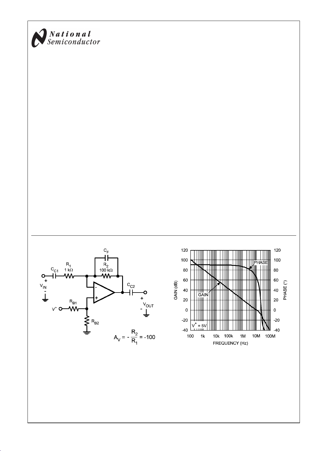
High Gain Wide Bandwidth Inverting Amplifier
© 2008 National Semiconductor Corporation 201238 www.national.com
20123861
Open Loop Gain and Phase vs. Frequency
20123806
Page 2
Absolute Maximum Ratings (Note 1)
If Military/Aerospace specified devices are required,
please contact the National Semiconductor Sales Office/
Distributors for availability and specifications.
ESD Tolerance (Note 2)
Human Body Model 2000V
Machine Model 100V
Differential Input V
Supply Voltage (VS = V+ - V−)
LMV651/LMV652/LMV654
Input/Output Pin Voltage V+ +0.3V, V− −0.3V
Storage Temperature Range −65°C to 150°C
Junction Temperature (Note 3) 150°C
Soldering Information
ID
±0.3V
6V
Infrared or Convection (20 sec) 235°C
Wave Soldering Lead Temp (10
sec) 260°C
Operating Ratings (Note 1)
Temperature Range (Note 3) −40°C to 125°C
Supply Voltage 2.7V to 5.5V
Package Thermal Resistance (θJA)(Note 3)
5-Pin SC70 456°C/W
5-Pin SOT-23 234°C/W
8-Pin MSOP 234°C/W
14-Pin TSSOP 160°C/W
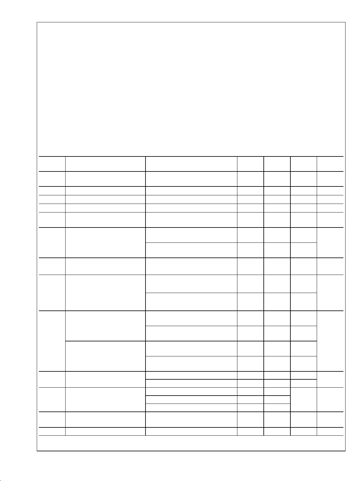
3V DC Electrical Characteristics
Unless otherwise specified, all limits are guaranteed for TA = 25°C, V+ = 3V, V− = 0V, VO = VCM = V+/2, and RL > 1 MΩ. Bold-
face limits apply at the temperature extremes.
Symbol Parameter Conditions Min
(Note 5)
V
OS
TC V
I
B
I
OS
CMRR Common Mode Rejection Ratio
PSRR Power Supply Rejection Ratio
CMVR Input Common-Mode Voltage
A
VOL
V
O
I
SC
I
S
SR Slew Rate AV = +1,
GBW Gain Bandwidth Product 12 MHz
Input Offset Voltage 0.1 ±1.5
Input Offset Average Drift 6.6
OS
Input Bias Current (Note 6) 80 120 nA
Input Offset Current 2.2 15
0 ≤ V
3.0 ≤ V+ ≤ 5V, VCM = 0.5
2.7 ≤ V+ ≤ 5.5V, VCM = 0.5
Range
Large Signal Voltage Gain
Output Swing High
Output Swing Low
Maximum Continuous Output
Current
Supply Current per Amplifier LMV651 115 140
CMRR ≥ 75 dB
CMRR ≥ 60 dB
0.3 ≤ VO ≤ 2.7, RL = 2 kΩ to V+/2
0.4 ≤ VO ≤ 2.6, RL = 2 kΩ to V+/2
0.3 ≤ VO ≤ 2.7, RL = 10 kΩ to V+/2
0.4 ≤ VO ≤ 2.6, RL = 10 kΩ to V+/2
RL = 2 kΩ to V+/2
RL = 10 kΩ to V+/2
RL = 2 kΩ to V+/2
RL = 10 kΩ to V+/2
Sourcing (Note 8) 17
Sinking (Note 8) 25
LMV652 118
LMV654 122
10% to 90% (Note 7)
≤ 2.0 V
CM
87
80
87
81
87
81
0
0
80
76
86
83
80 95
45 50
95 110
60 65
3.0
Typ
(Note 4)
100 dB
95 dB
95
2.1
85
93
Max
(Note 5)
2.7
2.1
120
60
125
75
175
Units
mV
μV/°C
nA
V
dB
mV from
rail
mA
μA
V/μs
www.national.com 2
Page 3
LMV651/LMV652/LMV654
Symbol Parameter Conditions Min
(Note 5)
e
n
Input-Referred Voltage Noise f = 100 kHz 17
f = 1 kHz 17
i
n
Input-Referred Current Noise f = 100 kHz 0.1
f = 1 kHz 0.15
THD Total Harmonic Distortion
f = 1 kHz, AV = 2, RL = 2 kΩ
0.003 %
Typ
(Note 4)
Max
(Note 5)
Units
nV/
pA/
5V DC Electrical Characteristics
Unless otherwise specified, all limits are guaranteed for TJ = 25°C, V+ = 5V, V− = 0V,VO = VCM = V+/2, and RL > 1 MΩ. Boldface
limits apply at the temperature extremes.
Symbol Parameter Conditions Min
(Note 5)
V
OS
TC V
I
B
I
OS
CMRR Common Mode Rejection Ratio
PSRR Power Supply Rejection Ratio
Input Offset Voltage 0.1 ±1.5
Input Offset Average Drift 6.6
OS
Input Bias Current (Note 6) 80 120 nA
Input Offset Current 2.2 15
0 ≤ V
≤ 4.0 V
CM
3V ≤ V+ ≤ 5V, VCM = 0.5V
90
83
87
81
2.7V ≤ V+ ≤ 5.5V, VCM = 0.5V
87
81
CMVR Input Common-Mode Voltage
Range
A
VOL
V
O
Large Signal Voltage Gain
Output Swing High
Output Swing Low
I
SC
Maximum Continuous Output
Current
I
S
Supply Current per Amplifier LMV651 116 140
CMRR ≥ 80 dB
CMRR ≥ 68 dB
0.3 ≤ VO ≤ 4.7V, RL = 2 kΩ to V+/2
0.4 ≤ VO ≤ 4.6, RL = 2 kΩ to V+/2
0.3 ≤ VO ≤ 4.7V, RL = 10 kΩ to V+/2
0.4 ≤ VO ≤ 4.6, RL = 10 kΩ to V+/2
RL = 2 kΩ to V+/2
RL = 10 kΩ to V+/2
RL = 2 kΩ to V+/2
RL = 10 kΩ to V+/2
Sourcing (Note 8) 18.5
Sinking (Note 8) 25
0
0
79
76
87
84
120 140
75 90
110 130
70 80
LMV652 118
LMV654 122
SR Slew Rate AV = +1, VO = 1 V
PP
3.0
10% to 90% (Note 7)
GBW Gain Bandwidth Product 12 MHz
e
n
Input-Referred Voltage Noise f = 100 kHz 17
f = 1 kHz 17
i
n
Input-Referred Current Noise f = 100 kHz 0.1
f = 1 kHz 0.15
THD Total Harmonic Distortion
f = 1 kHz, AV = 2, RL = 2 kΩ
0.003 %
Typ
(Note 4)
Max
(Note 5)
2.7
100 dB
95 dB
95
4.1
4.1
84
94
185
120
150
95
175
nV/
pA/
Units
mV
μV/°C
nA
V
dB
mV from
rail
mA
μA
V/μs
3 www.national.com
Page 4
Note 1: Absolute Maximum Ratings indicate limits beyond which damage to the device may occur. Operating Ratings indicate conditions for which the device is
intended to be functional, but specific performance is not guaranteed. For guaranteed specifications and the test conditions, see the Electrical Characteristics
Tables.
Note 2: Human Body Model, applicable std. MIL-STD-883, Method 3015.7. Machine Model, applicable std. JESD22-A115-A (ESD MM std. of JEDEC)
Field-Induced Charge-Device Model, applicable std. JESD22-C101-C (ESD FICDM std. of JEDEC).
Note 3: The maximum power dissipation is a function of T
PD = (T
Note 4: Typical values represent the most likely parametric norm as determined at the time of characterization. Actual typical values may vary over time and will
also depend on the application and configuration. The typical values are not tested and are not guaranteed on shipped production material.
Note 5: Limits are 100% production tested at 25°C. Limits over the operating temperature range are guaranteed through correlations using Statistical Quality
Control (SQC) method.
Note 6: Positive current corresponds to current flowing into the device.
LMV651/LMV652/LMV654
Note 7: Slew rate is the average of the rising and falling slew rates.
Note 8: The part is not short circuit protected and is not recommended for operation with low resistive loads. Typical sourcing and sinking output current curves
are provided in the Typical Performance Characteristics and should be consulted before designing for heavy loads.
- TA)/ θJA. All numbers apply for packages soldered directly onto a PC board.
J(MAX)
, θJA, and TA. The maximum allowable power dissipation at any ambient temperature is
J(MAX
Connection Diagrams
5-Pin SC70/ SOT-23
Top View
20123802
8-Pin MSOP
Top View
14-Pin TSSOP
20123803
Top View
Ordering Information
Package Part Number Package Marking Transport Media NSC Drawing
5-Pin SC70
5-Pin SOT-23
8-Pin MSOP
14-Pin TSSOP
LMV651MG
LMV651MGX 3k Units Tape and Reel
LMV651MF
LMV651MFX 3k Units Tape and Reel
LMV652MM
LMV652MMX 3.5k Units Tape and Reel
LMV654MT
LMV654MTX 2.5k Units Tape and Reel
A93
AY2A
AB3A
LMV654MT
1k Units Tape and Reel
1k Units Tape and Reel
1k Units Tape and Reel
94 Units/Rail
MAA05A
MF05A
MUA08A
MTC14
20123804
www.national.com 4
Page 5
LMV651/LMV652/LMV654
Typical Performance Characteristics Unless otherwise specified, T
VCM= VS/2
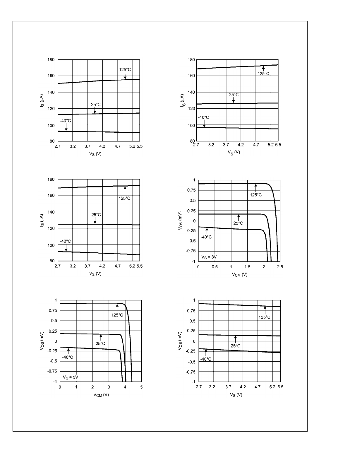
Supply Current vs. Supply Voltage (LMV651)
20123834
Supply Current per Channel vs. Supply Voltage (LMV654)
Supply Current per Channel vs. Supply Voltage (LMV652)
VOS vs. V
= 25°C, VS= 5V, V+= 5V, V−= 0V,
A
20123865
CM
VOS vs. V
CM
20123864
20123826
20123825
VOS vs. Supply Voltage
20123821
5 www.national.com
Page 6

I
BIAS
LMV651/LMV652/LMV654
vs. V
CM
I
BIAS
vs. V
CM
20123823
I
vs. Supply Voltage
BIAS
20123822
Negative Output Swing vs. Supply Voltage
20123824
Positive Output Swing vs. Supply Voltage
20123828
Positive Output Swing vs. Supply Voltage
20123829
www.national.com 6
20123827
Page 7

LMV651/LMV652/LMV654
Negative Output Swing vs. Supply Voltage
20123830
Sinking Current vs. Output Voltage (LMV651)
Sourcing Current vs. Output Voltage
20123832
Sinking Current vs. Output Voltage (LMV652)
20123833
Sinking Current vs. Output Voltage (LMV654)
20123863
20123866
Open Loop Gain and Phase with Capacitive Load
20123811
7 www.national.com
Page 8

Open Loop Gain and Phase with Resistive Load
LMV651/LMV652/LMV654
Phase Margin vs. Capacitive Load (Stability)
20123812
Input Referred Voltage Noise vs. Frequency
20123814
Slew Rate vs. Supply Voltage
20123813
Input Referred Current Noise vs. Frequency
20123815
THD+N vs. V
OUT
20123816
www.national.com 8
20123809
Page 9

LMV651/LMV652/LMV654
THD+N vs. V
OUT
THD+N vs. Frequency
20123810
THD+N vs. Frequency
20123807
Small Signal Transient Response
Small Signal Transient Response
20123808
20123817
20123818
Large Signal Transient Response
20123819
9 www.national.com
Page 10

PSRR vs. Frequency
LMV651/LMV652/LMV654
CMRR vs. Frequency
20123835
Closed Loop Output Impedance vs. Frequency
20123837
20123836
www.national.com 10
Page 11

Application Information
ADVANTAGES OF THE LMV651/LMV652/LMV654
Low Voltage and Low Power Operation
The LMV651/LMV652/LMV654 have performance guaranteed at supply voltages of 3V and 5V. These parts are guaranteed to be operational at all supply voltages between 2.7V
and 5.5V. The LMV651 draws a low supply current of 116
μA, the LMV652 draws 118 μA/channel and the LMV654
draws 122 μA/channel. This family of op amps provides the
low voltage and low power amplification which is essential for
portable applications.
Wide Bandwidth
Despite drawing the very low supply current of 116 µA, the
LMV651/LMV652/LMV654 manage to provide a wide unity
gain bandwidth of 12 MHz. This is easily one of the best
bandwidth to power ratios ever achieved, and allows these op
amps to provide wideband amplification while using the minimum amount of power. This makes this family of parts ideal
for low power signal processing applications such as portable
media players and other accessories.
Low Input Referred Noise
The LMV651/LMV652/LMV654 provide a flatband input referred voltage noise density of 17 nV/
cantly better than the noise performance expected from a low
power op amp. These op amps also feature exceptionally low
1/f noise, with a very low 1/f noise corner frequency of 4 Hz.
This makes these parts ideal for low power applications which
require decent noise performance, such as PDAs and
portable sensors.
Ground Sensing and Rail-to-Rail Output
The LMV651/LMV652/LMV654 each have a rail-to-rail output
stage, which provides the maximum possible output dynamic
range. This is especially important for applications requiring
a large output swing. The input common mode range of this
family of devices includes the negative supply rail which allows direct sensing at ground in a single supply operation.
Small Size
The small footprint of the packages for the LMV651/LMV652/
LMH654 saves space on printed circuit boards, and enables
the design of smaller and more compact electronic products.
Long traces between the signal source and the op amp make
the signal path susceptible to noise. By using a physically
smaller package, these op amps can be placed closer to the
signal source, reducing noise pickup and enhancing signal
integrity.
, which is signifi-
LMV651/LMV652/LMV654
20123859
FIGURE 1. Gain vs. Frequency for an Op Amp
An op amp, ideally, has a dominant pole close to DC, which
causes its gain to decay at the rate of 20 dB/decade with respect to frequency. If this rate of decay, also known as the
rate of closure (ROC), remains the same until the op amp's
unity gain bandwidth, the op amp is stable. If, however, a large
capacitance is added to the output of the op amp, it combines
with the output impedance of the op amp to create another
pole in its frequency response before its unity gain frequency
(Figure 1). This increases the ROC to 40 dB/decade and
causes instability.
In such a case a number of techniques can be used to restore
stability to the circuit. The idea behind all these schemes is to
modify the frequency response such that it can be restored to
an ROC of 20 dB/decade, which ensures stability.
In The Loop Compensation
Figure 2 illustrates a compensation technique, known as ‘in
the loop’ compensation, that employs an RC feedback circuit
within the feedback loop to stabilize a non-inverting amplifier
configuration. A small series resistance, RS, is used to isolate
the amplifier output from the load capacitance, CL, and a small
capacitance, CF, is inserted across the feedback resistor to
bypass CL at higher frequencies.
STABILITY OF OP AMP CIRCUITS
Stability and Capacitive Loading
If the phase margin of the LMV651/LMV652/LMV654 is plotted with respect to the capacitive load (CL) at its output, it is
seen that the phase margin reduces significantly if CL is increased beyond 100 pF. This is because the op amp is
designed to provide the maximum bandwidth possible for a
low supply current. Stabilizing it for higher capacitive loads
would have required either a drastic increase in supply current, or a large internal compensation capacitance, which
would have reduced the bandwidth of the op amp. Hence, if
these devices are to be used for driving higher capacitive
loads, they would have to be externally compensated.
20123858
FIGURE 2. In the Loop Compensation
11 www.national.com
Page 12

The values for RS and CF are decided by ensuring that the
zero attributed to CF lies at the same frequency as the pole
attributed to CL. This ensures that the effect of the second
pole on the transfer function is compensated for by the presence of the zero, and that the ROC is maintained at 20 dB/
decade. For the circuit shown in Figure 2 the values of RS and
CF are given by Equation 1. Values of RS and CF required for
maintaining stability for different values of CL, as well as the
phase margins obtained, are shown in Table 1. RF and R
are taken to be 10 kΩ, RL is 2 kΩ, while R
340Ω.
OUT
LMV651/LMV652/LMV654
TABLE 1.
CL (pF)
RS (Ω)
150 340 15 39.4
200 340 20 34.6
250 340 25 31.1
Although this methodology provides circuit stability for any
load capacitance, it does so at the price of bandwidth. The
closed loop bandwidth of the circuit is now limited by RF and
CF.
CF (pF) Phase Margin (°)
is taken as
(1)
than 0.003% distortion. Two amplifier circuits are shown in
Figure 4 and Figure 5. Figure 4 is an inverting amplifier, with
a 100 kΩ feedback resistor, R2, and a 1 kΩ input resistor,
R1, and provides a gain of −100. With the LMV651/LMV652/
LMV654 these circuits can provide gain of −100 with a −3 dB
bandwidth of 120 kHz, for a quiescent current as low as 116
μA. Similarly, the circuit in Figure 5, a non-inverting amplifier
with a gain of 1001, can provide that gain with a −3 dB band-
IN
width of 12 kHz, for a similar low quiescent power dissipation.
Coupling capacitors CC1 and CC2 can be added to isolate the
circuit from DC voltages, while RB1 and RB2 provide DC biasing. A feedback capacitor CF can also be added to improve
compensation.
Compensation By External Resistor
In some applications it is essential to drive a capacitive load
without sacrificing bandwidth. In such a case, in the loop compensation is not viable. A simpler scheme for compensation
is shown in Figure 3. A resistor, R
tween the load capacitance and the output. This introduces a
, is placed in series be-
ISO
zero in the circuit transfer function, which counteracts the effect of the pole formed by the load capacitance, and ensures
stability. The value of R
pending on the size of CL and the level of performance de-
to be used should be decided de-
ISO
sired. Values ranging from 5Ω to 50Ω are usually sufficient to
ensure stability. A larger value of R
with lesser ringing and overshoot, but will also limit the output
will result in a system
ISO
swing and the short circuit current of the circuit.
20123860
FIGURE 3. Compensation by Isolation Resistor
Typical Applications
HIGH GAIN LOW POWER AMPLIFIERS
With a low supply current, low power operation, and low harmonic distortion, the LMV651/LMV652/LMV654 are ideal for
wide-bandwidth, high gain amplification. The wide unity gain
bandwidth allows these parts to provide large gain over a wide
frequency range, while driving loads as low as 2 kΩ with less
20123861
FIGURE 4. High Gain Inverting Amplifier
20123862
FIGURE 5. High Gain Non-Inverting Amplifier
ACTIVE FILTERS
With a wide unity gain bandwidth of 12 MHz, low input referred
noise density and a low power supply current, the LMV651/
LMV652/LMV654 are well suited for low-power filtering applications. Active filter topologies, like the Sallen-Key low pass
filter shown in Figure 6, are very versatile, and can be used
to design a wide variety of filters (Chebyshev, Butterworth or
Bessel). The Sallen-Key topology, in particular, can be used
to attain a wide range of Q, by using positive feedback to reject the undesired frequency range.
www.national.com 12
Page 13

In the circuit shown in Figure 6, the two capacitors appear as
open circuits at lower frequencies and the signal is simply
buffered to the output. At high frequencies the capacitors appear as short circuits and the signal is shunted to ground by
one of the capacitors before it can be amplified. Near the cutoff frequency, where the impedance of the capacitances is on
the same order as Rg and Rf, positive feedback through the
other capacitor allows the circuit to attain the desired Q. The
ratio of the two resistors, m2, provides a knob to control the
value of Q obtained.
20123820
FIGURE 6. Sallen-Key Low Pass Filter
LMV651/LMV652/LMV654
13 www.national.com
Page 14

Physical Dimensions inches (millimeters) unless otherwise noted
LMV651/LMV652/LMV654
NS Package Number MAA05A
5-Pin SC70
5-Pin SOT-23
NS Package Number MF05A
www.national.com 14
Page 15

LMV651/LMV652/LMV654
NS Package Number MUA08A
8-Pin MSOP
14-Pin TSSOP
NS Package Number MTC14
15 www.national.com
Page 16

Notes
For more National Semiconductor product information and proven design tools, visit the following Web sites at:
Products Design Support
Amplifiers www.national.com/amplifiers WEBENCH www.national.com/webench
Audio www.national.com/audio Analog University www.national.com/AU
Clock Conditioners www.national.com/timing App Notes www.national.com/appnotes
Data Converters www.national.com/adc Distributors www.national.com/contacts
Displays www.national.com/displays Green Compliance www.national.com/quality/green
Ethernet www.national.com/ethernet Packaging www.national.com/packaging
Interface www.national.com/interface Quality and Reliability www.national.com/quality
LVDS www.national.com/lvds Reference Designs www.national.com/refdesigns
Power Management www.national.com/power Feedback www.national.com/feedback
Switching Regulators www.national.com/switchers
LDOs www.national.com/ldo
LED Lighting www.national.com/led
PowerWise www.national.com/powerwise
Serial Digital Interface (SDI) www.national.com/sdi
Temperature Sensors www.national.com/tempsensors
Wireless (PLL/VCO) www.national.com/wireless
THE CONTENTS OF THIS DOCUMENT ARE PROVIDED IN CONNECTION WITH NATIONAL SEMICONDUCTOR CORPORATION
(“NATIONAL”) PRODUCTS. NATIONAL MAKES NO REPRESENTATIONS OR WARRANTIES WITH RESPECT TO THE ACCURACY
OR COMPLETENESS OF THE CONTENTS OF THIS PUBLICATION AND RESERVES THE RIGHT TO MAKE CHANGES TO
SPECIFICATIONS AND PRODUCT DESCRIPTIONS AT ANY TIME WITHOUT NOTICE. NO LICENSE, WHETHER EXPRESS,
IMPLIED, ARISING BY ESTOPPEL OR OTHERWISE, TO ANY INTELLECTUAL PROPERTY RIGHTS IS GRANTED BY THIS
DOCUMENT.
TESTING AND OTHER QUALITY CONTROLS ARE USED TO THE EXTENT NATIONAL DEEMS NECESSARY TO SUPPORT
NATIONAL’S PRODUCT WARRANTY. EXCEPT WHERE MANDATED BY GOVERNMENT REQUIREMENTS, TESTING OF ALL
PARAMETERS OF EACH PRODUCT IS NOT NECESSARILY PERFORMED. NATIONAL ASSUMES NO LIABILITY FOR
APPLICATIONS ASSISTANCE OR BUYER PRODUCT DESIGN. BUYERS ARE RESPONSIBLE FOR THEIR PRODUCTS AND
APPLICATIONS USING NATIONAL COMPONENTS. PRIOR TO USING OR DISTRIBUTING ANY PRODUCTS THAT INCLUDE
NATIONAL COMPONENTS, BUYERS SHOULD PROVIDE ADEQUATE DESIGN, TESTING AND OPERATING SAFEGUARDS.
EXCEPT AS PROVIDED IN NATIONAL’S TERMS AND CONDITIONS OF SALE FOR SUCH PRODUCTS, NATIONAL ASSUMES NO
LIABILITY WHATSOEVER, AND NATIONAL DISCLAIMS ANY EXPRESS OR IMPLIED WARRANTY RELATING TO THE SALE
AND/OR USE OF NATIONAL PRODUCTS INCLUDING LIABILITY OR WARRANTIES RELATING TO FITNESS FOR A PARTICULAR
PURPOSE, MERCHANTABILITY, OR INFRINGEMENT OF ANY PATENT, COPYRIGHT OR OTHER INTELLECTUAL PROPERTY
RIGHT.
LMV651/LMV652/LMV654 12 MHz, Low Voltage, Low Power Amplifiers
LIFE SUPPORT POLICY
NATIONAL’S PRODUCTS ARE NOT AUTHORIZED FOR USE AS CRITICAL COMPONENTS IN LIFE SUPPORT DEVICES OR
SYSTEMS WITHOUT THE EXPRESS PRIOR WRITTEN APPROVAL OF THE CHIEF EXECUTIVE OFFICER AND GENERAL
COUNSEL OF NATIONAL SEMICONDUCTOR CORPORATION. As used herein:
Life support devices or systems are devices which (a) are intended for surgical implant into the body, or (b) support or sustain life and
whose failure to perform when properly used in accordance with instructions for use provided in the labeling can be reasonably expected
to result in a significant injury to the user. A critical component is any component in a life support device or system whose failure to perform
can be reasonably expected to cause the failure of the life support device or system or to affect its safety or effectiveness.
National Semiconductor and the National Semiconductor logo are registered trademarks of National Semiconductor Corporation. All other
brand or product names may be trademarks or registered trademarks of their respective holders.
Copyright© 2008 National Semiconductor Corporation
For the most current product information visit us at www.national.com
www.national.com
National Semiconductor
Americas Technical
Support Center
Email: support@nsc.com
Tel: 1-800-272-9959
National Semiconductor Europe
Technical Support Center
Email: europe.support@nsc.com
German Tel: +49 (0) 180 5010 771
English Tel: +44 (0) 870 850 4288
National Semiconductor Asia
Pacific Technical Support Center
Email: ap.support@nsc.com
National Semiconductor Japan
Technical Support Center
Email: jpn.feedback@nsc.com
 Loading...