

Page 1
LMV431/LMV431A
Low-Voltage (1.24V) Adjustable Precision Shunt
Regulators
LMV431/LMV431A Low-Voltage (1.24V) Adjustable Precision Shunt Regulators
January 2000
General Description
The LMV431and LMV431A are precision 1.24V shunt regulators capableof adjustment to 30V. Negative feedback from
the cathode to the adjust pin controls the cathode voltage,
much like a non-inverting op amp configuration (Refer to
Symbol and Functional diagrams). A two resistor voltage divider terminated atthe adjust pin controls the gain of a 1.24V
band-gap reference. Shorting the cathode to the adjust pin
(voltage follower) provides a cathode voltage of a 1.24V.
The LMV431 and LMV431A have respective initial tolerances of 1.5%and 1%. Both grades are available in commercial and Industrial temperature ranges.
The LMV431 and LMV431A functionally lends themselves to
several applications that require zener diode type performance at low voltages. Applications include a 3V to 2.7V low
drop-out regulator, an error amplifier in a 3V off-line switching regulator and even as a voltage detector. The part is typically stable with capacitive loads greater than 10nF and less
than 50 pF.
The LMV431 and LMV431A provide performance at a competitive price.
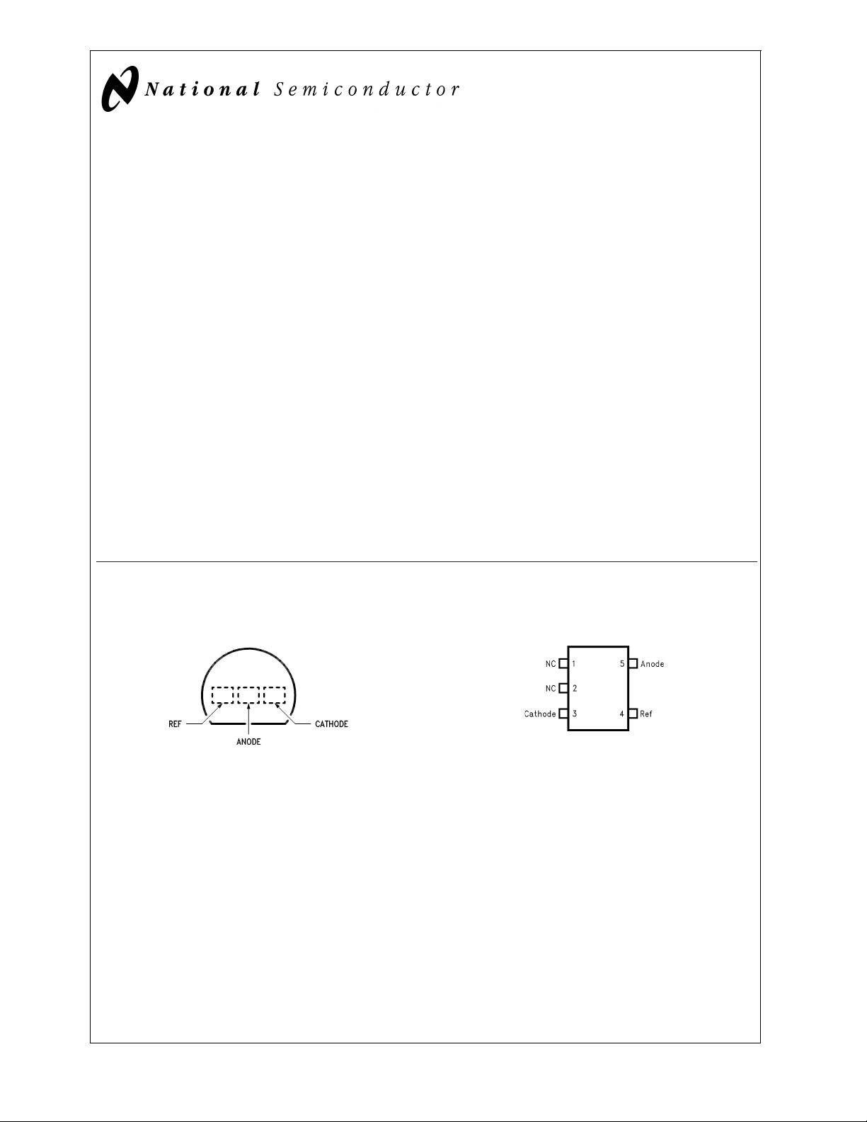
Connection Diagrams
TO92: Plastic Package
Features
n Low Voltage Operation/Wide Adjust Range (1.24V/30V)
n 1%Initial Tolerance (LMV431A)
n Temperature Compensated for Industrial Temperature
Range (39 PPM/˚C for the LMV431AI)
n Low Operation Current (55µA)
n Low Output Impedance (0.25Ω)
n Fast Turn-On Response
n Low Cost
Applications
n Shunt Regulator
n Series Regulator
n Current Source or Sink
n Voltage Monitor
n Error Amplifier
n 3V Off-Line Switching Regulator
n Low Dropout N-Channel Series Regulator
SOT23-5
DS100958-1
Top View
© 2000 National Semiconductor Corporation DS100958 www.national.com
Top View
DS100958-44
Page 2
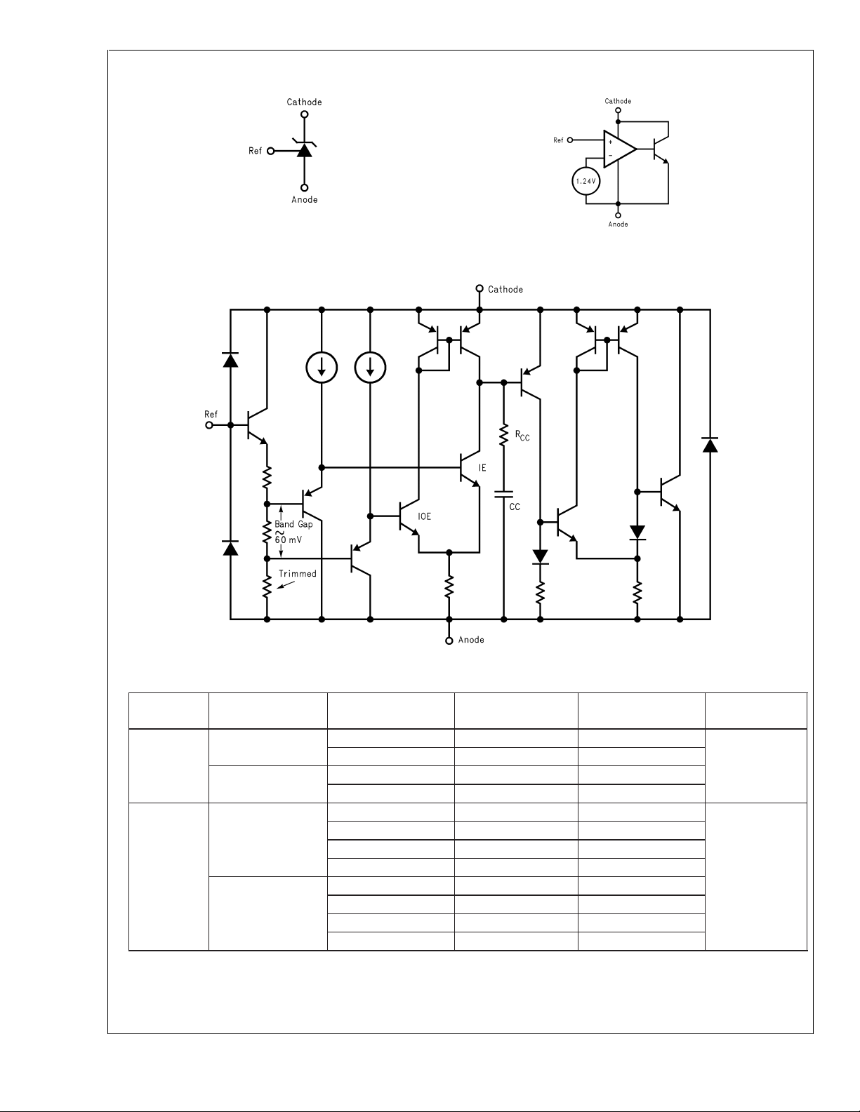
Symbol and Functional Diagrams
LMV431/LMV431A
DS100958-59
Simplified Schematic
DS100958-60
Ordering Information
Package Temperature
Range
TO92 Industrial Range
−40˚C to +85˚C
Commerial Range
0˚C to +70˚C
SOT23-5 Industrial Range
−40˚C to +85˚C
Commercial Range
0˚C to +70˚C
www.national.com 2
Voltage Tolerance Part Number Package Marking Drawing
%
1
%
1.5
%
1
%
1.5
%
1
%
1
%
1.5
%
1.5
%
1
%
1
%
1.5
%
1.5
LMV431AIZ LMV431AIZ
LMV431IZ LMV431IZ
LMV431ACZ LMV431ACZ
LMV431CZ LMV431CZ
LMV431AIM5 N08A
LMV431AIM5X N08A
LMV431IM5 N08B
LMV431IM5X N08B
LMV431ACM5 N09A
LMV431ACM5X N09A
LMV431CM5 N09B
LMV431CM5X N09B
DS100958-3
Number
Z03A
MA05A
Page 3
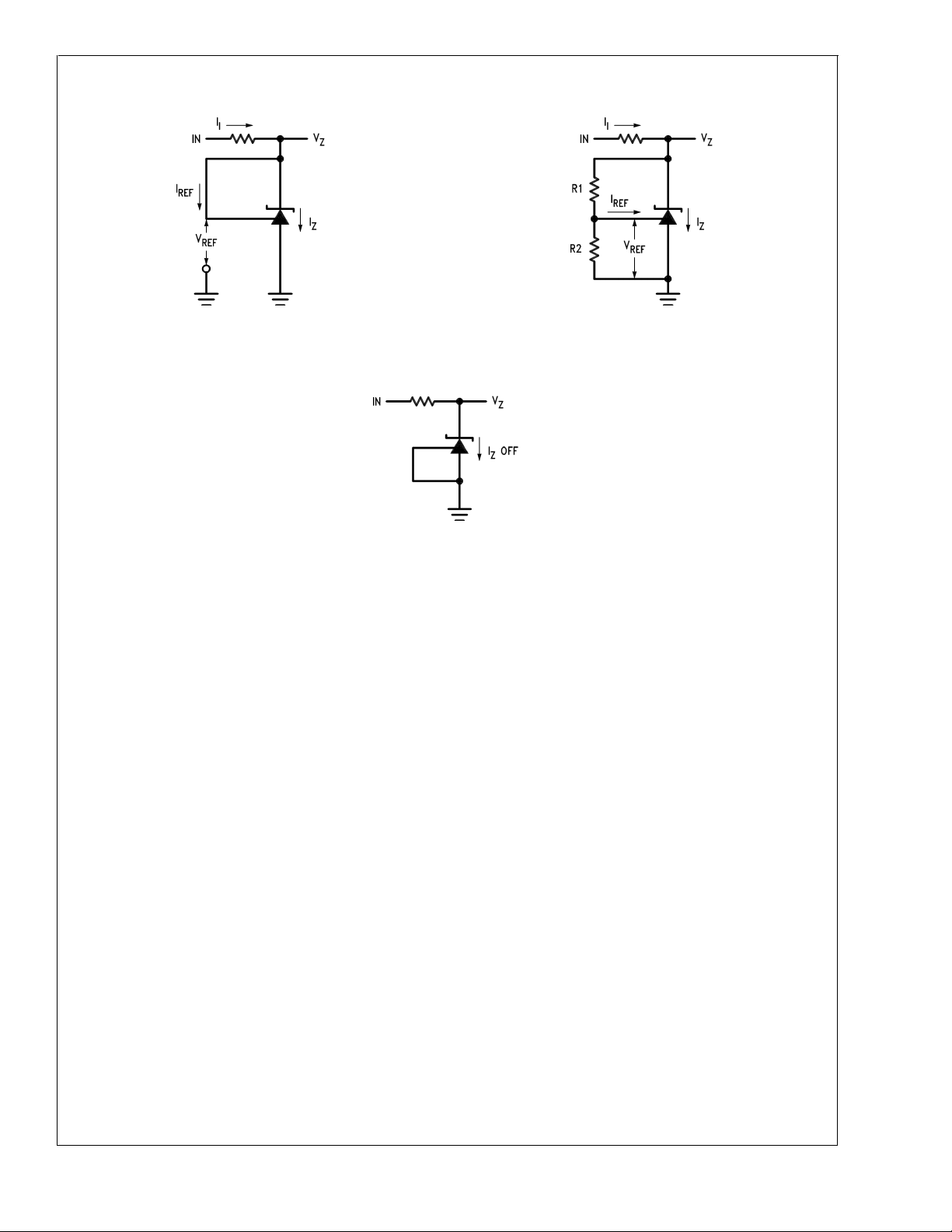
DC/AC Test Circuits for Table and Curves
LMV431/LMV431A
DS100958-4
FIGURE 1. Test Circuit for V
=
V
Z
REF
Note: V
=
Z
(1 + R1/R2) + I
V
REF
FIGURE 2. Test Circuit for V
DS100958-6
FIGURE 3. Test Circuit for Off-State Current
REF
•
R1
DS100958-5
>
V
Z
REF
www.national.com3
Page 4
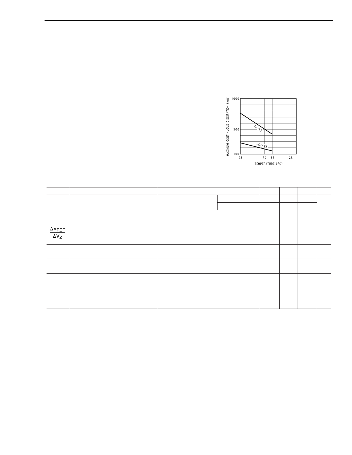
Absolute Maximum Ratings (Note 1)
If Military/Aerospace specified devices are required,
please contact the National Semiconductor Sales Office/
Distributors for availability and specifications.
Storage Temperature Range −65˚C to +150˚C
Operating Temperature Range
LMV431/LMV431A
Industrial (LMV431AI, LMV431I) −40˚C to +85˚C
Commercial (LMV431AC, LMV431C) 0˚C to +70˚C
Lead Temperature
Operating Conditions
Cathode Voltage V
Cathode Current 0.1 mA to 15mA
Temperature range
LMV431AI −40˚C ≤ T
Thermal Resistance (θ
)(Note 3)
JA
SOT23-5 Package 455 ˚C/W
TO-92 Package 161 ˚C/W
Derating Curve (Slope=−1/θ
)
JA
REF
to 30V
TO92 Package/SOT23 -5Package
(Soldering, 10 sec.) 265˚C
Internal Power Dissipation (Note 2)
TO92
0.78W
SOT23-5 Package 0.28W
Cathode Voltage 35V
Continuous Cathode Current −30 mA to +30mA
Reference Input Current range −.05mA to 3mA
DS100958-30
LMV431C Electrical Characteristics
=
T
25˚C unless otherwise specified
A
Symbol Parameter Conditions Min Typ Max Units
V
REF
V
DEV
I
REF
∝
I
Z(MIN)
I
Z(OFF)
r
Z
I
Reference Voltage V
Deviation of Reference Input Voltage
Over Temperature (Note 4)
Ratio of the Change in Reference
Voltage to the Change in Cathode
Voltage
Reference Input Current R
Deviation of Reference Input Current
REF
over Temperature
Minimum Cathode Current for
Regulation
Off-State Current V
Dynamic Output Impedance (Note 5) V
=
V
Z
(See Figure 1 )
=
V
Z
=
Full Range
T
A
=
I
Z
VZfrom V
=
R
1
=
1
=
I
10mA
I
=
R
1
=
10mA, T
I
I
=
V
Z
=
6V, V
Z
=
Z
Frequency=0Hz
REF,IZ
V
REF,IZ
10mA
REF
10k, R
10kΩ,R
10kΩ,R
V
REF
REF
V
REF,IZ
(see Figure 2)
=
10mA
=
10mA,
(See Figure 1)
(see Figure 2 )
to 6V
=
∞
and 2.6K
2
=
∞
2
=
∞
,
2
=
Full Range
A
(see Figure 1)
=
(see Figure 3 )
0V
=
0.1mA to 15mA
(see Figure 1)
TA= 25˚C 1.222 1.24 1.258
T
= Full Range 1.21 1.27 V
A
412mV
−1.5 −2.7 mV/V
0.15 0.5 µA
(see Figure 2)
0.05 0.3 µA
55 80 µA
0.001 0.1 µA
0.25 0.4 Ω
≤ 85˚C
A
www.national.com 4
Page 5
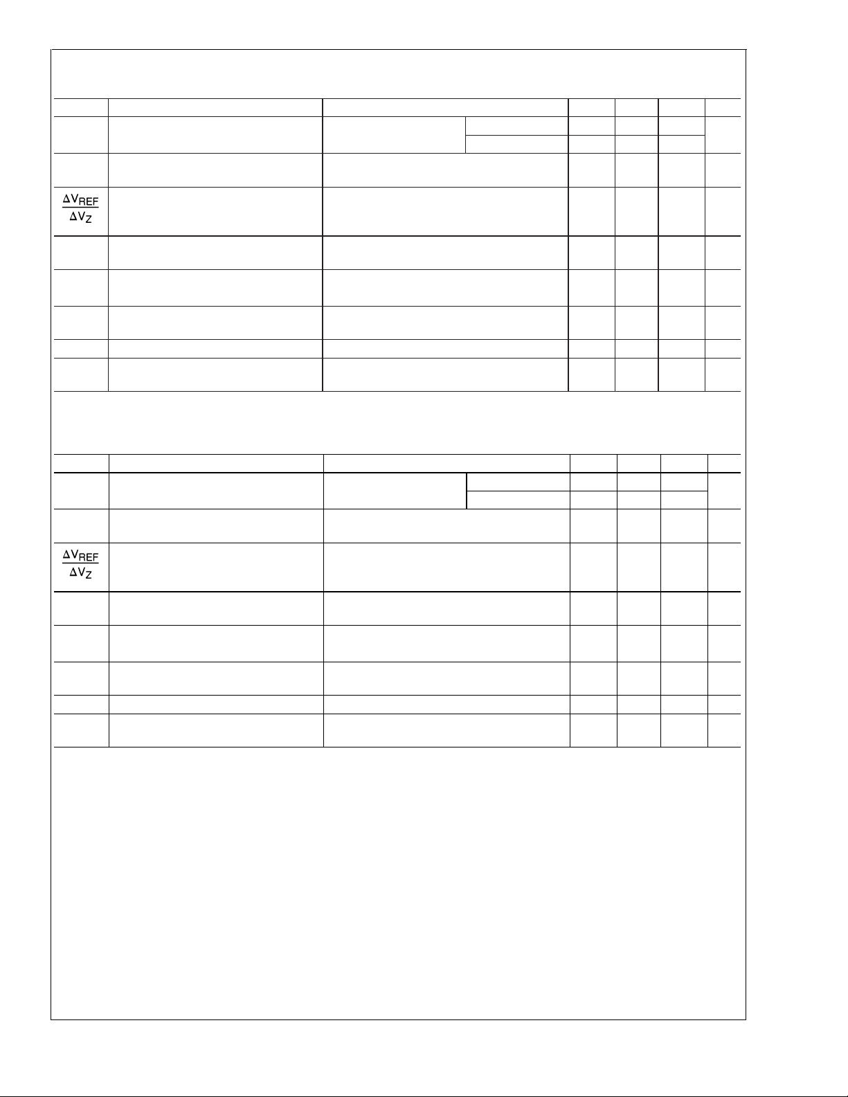
LMV431I Electrical Characteristics
=
T
25˚C unless otherwise specified
A
Symbol Parameter Conditions Min Typ Max Units
V
REF
V
DEV
I
REF
∝
I
Z(MIN)
I
Z(OFF)
r
Z
I
Reference Voltage V
Deviation of Reference Input Voltage
Over Temperature (Note 4)
Ratio of the Change in Reference
Voltage to the Change in Cathode
Voltage
Reference Input Current R
Deviation of Reference Input Current
REF
over Temperature
Minimum Cathode Current for
Regulation
Off-State Current V
Dynamic Output Impedance (Note 5) V
=
V
Z
(See Figure 1 )
=
V
Z
=
Full Range
T
A
=
I
Z
VZfrom V
=
R
1
=
1
=
I
10mA
I
=
R
1
=
10mA, T
I
I
=
V
Z
=
6V, V
Z
=
Z
Frequency=0Hz
REF,IZ
V
REF,IZ
10mA
REF
10k, R
10kΩ,R
(see Figure 2)
10kΩ,R
V
REF
REF
V
REF,IZ
=
10mA
=
10mA,
(See Figure 1)
(see Figure 2 )
to 6V
=
∞
and 2.6K
2
=
∞
2
=
∞
,
2
=
Full Range
A
(see Figure 1)
=
(see Figure 3 )
0V
=
0.1mA to 15mA
(see Figure 1)
TA= 25˚C 1.222 1.24 1.258
= Full Range 1.202 1.278
T
A
620mV
−1.5 −2.7 mV/V
0.15 0.5 µA
(see Figure 2)
0.1 0.4 µA
55 80 µA
0.001 0.1 µA
0.25 0.4 Ω
V
LMV431AC Electrical Characteristics
=
T
25˚C unless otherwise specified
A
Symbol Parameter Conditions Min Typ Max Units
V
REF
V
DEV
I
REF
∝
I
Z(MIN)
I
Z(OFF)
r
Z
I
Reference Voltage V
Deviation of Reference Input Voltage
Over Temperature (Note 4)
Ratio of the Change in Reference
Voltage to the Change in Cathode
Voltage
Reference Input Current R
Deviation of Reference Input Current
REF
over Temperature
Minimum Cathode Current for
Regulation
Off-State Current V
Dynamic Output Impedance (Note 5) V
=
V
Z
(See Figure 1 )
=
V
Z
=
Full Range
T
A
=
I
Z
VZfrom V
=
R
1
=
1
=
I
10 mA
I
=
R
1
=
10 mA, T
I
I
=
V
Z
=
6V, V
Z
=
Z
Frequency=0Hz
REF,IZ
V
REF,IZ
10 mA
REF
10k, R
10 kΩ,R
10 kΩ,R
(see Figure 1)
V
REF
REF
V
REF,IZ
=
10 mA
=
10mA,
(See Figure 1)
(see Figure 2 )
to 6V
=
∞
and 2.6K
2
=
∞
2
(see Figure 2)
=
∞
,
2
=
Full Range
A
=
(see Figure 3 )
0V
=
0.1mA to 15mA
(see Figure 1)
TA= 25˚C 1.228 1.24 1.252
= Full Range 1.221 1.259
T
A
412mV
−1.5 −2.7 mV/V
0.15 0.50 µA
(see Figure 2)
0.05 0.3 µA
55 80 µA
0.001 0.1 µA
0.25 0.4 Ω
V
LMV431/LMV431A
www.national.com5
Page 6

LMV431AI Electrical Characteristics
=
T
25˚C unless otherwise specified
A
Symbol Parameter Conditions Min Typ Max Units
V
REF
Reference Voltage V
=
V
Z
(See Figure 1 )
V
DEV
LMV431/LMV431A
Deviation of Reference Input Voltage
Over Temperature (Note 4)
Ratio of the Change in Reference
Voltage to the Change in Cathode
Voltage
I
∝
REF
I
REF
Reference Input Current R
Deviation of Reference Input Current
over Temperature
I
Z(MIN)
Minimum Cathode Current for
=
V
Z
=
Full Range
T
A
=
I
Z
VZfrom V
=
R
1
=
1
=
I
10mA
I
=
R
1
=
10mA, T
I
I
=
V
Z
Regulation
I
Z(OFF)
r
Z
Off-State Current V
Dynamic Output Impedance (Note 5) V
Z
Z
=
6V, V
=
Frequency=0Hz
Note 1: Absolute Maximum Ratings indicate limits beyond which damage to the device may occur. Electrical specifications do not apply when operating the device
beyond its rated operating conditions.
Note 2: Ratings apply to ambient temperature at 25˚C. Above this temperature, derate the TO92 at 6.2 mW/˚C, and the SOT23-5 at 2.2 mW/˚C. See derating curve
in Operating Condition section..
Note 3: T
Note 4: Deviation of reference input voltage, V
See following:
J Max
=
150˚C, T
=
+(θJAPD), where PDis the operating power of the device.
T
J
A
, is defined as the maximum variation of the reference input voltage over the full temperature range.
DEV
REF,IZ
V
REF,IZ
10mA
REF
10k, R
10kΩ,R
10kΩ,R
V
REF
REF
V
REF,IZ
(see Figure 2)
=
10mA
=
10mA,
(See Figure 1)
(see Figure 2 )
to 6V
=
∞
and 2.6K
2
=
∞
2
=
∞
,
2
=
Full Range
A
(see Figure 1)
=
(see Figure 3 )
0V
=
0.1mA to 15mA
(see Figure 1)
TA= 25˚C 1.228 1.24 1.252
T
= Full Range 1.215 1.265 V
A
620mV
−1.5 −2.7 mV/V
0.15 0.5 µA
(see Figure 2)
0.1 0.4 µA
55 80 µA
0.001 0.1 µA
0.25 0.4 Ω
www.national.com 6
Page 7

LMV431AI Electrical Characteristics (Continued)
The average temperature coefficient of the reference input voltage,∝V
, is defined as:
REF
LMV431/LMV431A
DS100958-7
Where:
=
T
∝
Example: V
Note 5: The dynamic output impedance, rZ, is defined as:
When the device is programmed with two external resistors, R1 and R2, (see
full temperature change.
2−T1
can be positive or negative depending on whether the slope is positive or negative.
V
REF
DEV
=
6.0mV,
REF
=
1240mV, T
2−T1
=
125˚C.
Figure 2
), the dynamic output impedance of the overall circuit, rZ, is defined as:
www.national.com7
Page 8

Typical Performance Characteristics
Reference Voltage vs. Junction Temperature
LMV431/LMV431A
Cathode Current vs. Cathode Voltage 1
DS100958-50
Reference Input Current vs. Junction Temperature
DS100958-62
Cathode Current vs. Cathode Voltage 2
Off-State Cathode Current vs.
Junction Temperature
DS100958-51
DS100958-63
DS100958-52
Delta Reference Voltage
Per Delta Cathode Voltage vs. Junction Temperature
DS100958-61
www.national.com 8
Page 9

Typical Performance Characteristics (Continued)
Input Voltage Noise vs. Frequency
LMV431/LMV431A
Low Frequency Peak to Peak Noise
DS100958-53
DS100958-54
DS100958-45
Test Circuit for Input Voltage
Noise vs Frequency
DS100958-64
Test Circuit for Peak to Peak
Noise (BW=0.1Hz to 10Hz)
Small Signal Voltage Gain and
Phase Shift vs. Frequency
DS100958-55
DS100958-46
Test Circuit For Voltage
Gain and Phase Shift
vs Frequency
www.national.com9
Page 10

Typical Performance Characteristics (Continued)
Reference Impedance vs Frequency
LMV431/LMV431A
DS100958-56
Pulse Response 1
DS100958-47
Test Circuit For Reference
Impedance vs Frequency
Pulse Response 2
DS100958-48
Test Circuit for
Pulse Response 1
DS100958-57
DS100958-49
Test Circuit for Pulse Response 2
DS100958-58
www.national.com 10
Page 11

Typical Performance Characteristics (Continued)
LMV431/LMV431A
Percentage Change in V
Extrapolated from life-test data taken at 125˚C; the activation energy assumed is 0.7eV.
vs Operating Life at 55˚C
REF
DS100958-66
www.national.com11
Page 12

Typical Applications
LMV431/LMV431A
Higher Current Shunt Regulator
Series Regulator
DS100958-16
Output Control of a Three
Terminal Fixed Regulator
DS100958-17
Crow Bar
DS100958-18
Over Voltage/Under Voltage
Protection Circuit
DS100958-19
DS100958-20
www.national.com 12
Page 13

Typical Applications (Continued)
LMV431/LMV431A
Voltage Monitor
DS100958-21
Delay Timer
Current Limiter or Current Source
DS100958-23
DS100958-22
Constant Current Sink
DS100958-24
www.national.com13
Page 14

Physical Dimensions inches (millimeters) unless otherwise noted
LMV431/LMV431A
SOT23-5 Molded Small Outline Transistor Package (M5)
Order Number LMV431AIM5, LMV431AIM5X,LMV431IM5, LMV431IM5X,
LMV431ACM5, LMV431ACM5X, LMV431CM5 and LMV431CM5X
NS Package Number MA05A
www.national.com 14
Page 15

Physical Dimensions inches (millimeters) unless otherwise noted (Continued)
LMV431/LMV431A Low-Voltage (1.24V) Adjustable Precision Shunt Regulators
Order Number LMV431AIZ, LMV431IZ, LMV431ACZ and LMV431CZ
NS Package Number Z03A
LIFE SUPPORT POLICY
NATIONAL’S PRODUCTS ARE NOT AUTHORIZED FOR USE AS CRITICAL COMPONENTS IN LIFE SUPPORT
DEVICES OR SYSTEMS WITHOUT THE EXPRESS WRITTEN APPROVAL OF THE PRESIDENT AND GENERAL
COUNSEL OF NATIONAL SEMICONDUCTOR CORPORATION. As used herein:
1. Life support devices or systems are devices or
systems which, (a) are intended for surgical implant
into the body, or (b) support or sustain life, and
whose failure to perform when properly used in
accordance with instructions for use provided in the
2. A critical component is any component of a life
support device or system whose failure to perform
can be reasonably expected to cause the failure of
the life support device or system, or to affect its
safety or effectiveness.
labeling, can be reasonably expected to result in a
significant injury to the user.
National Semiconductor
Corporation
Americas
Tel: 1-800-272-9959
Fax: 1-800-737-7018
Email: support@nsc.com
www.national.com
National does not assume any responsibility for use of any circuitry described, no circuit patent licenses are implied and National reserves the right at any time without notice to change said circuitry and specifications.
National Semiconductor
Europe
Fax: +49 (0) 1 80-530 85 86
Email: europe.support@nsc.com
Deutsch Tel: +49 (0) 1 80-530 85 85
English Tel: +49 (0) 1 80-532 78 32
Français Tel: +49 (0) 1 80-532 93 58
Italiano Tel: +49 (0) 1 80-534 16 80
National Semiconductor
Asia Pacific Customer
Response Group
Tel: 65-2544466
Fax: 65-2504466
Email: sea.support@nsc.com
National Semiconductor
Japan Ltd.
Tel: 81-3-5639-7560
Fax: 81-3-5639-7507
 Loading...