

Page 1
March 2003
LMV341/LMV342/LMV344
Single with Shutdown/Dual/Quad General Purpose, 2.7V,
Rail-to-Rail Output, 125˚C, Operational Amplifiers
General Description
The LMV341/342/344 are single, dual, and quad low voltage, and low power Operational Amplifiers. They are designed specifically for low voltage portable applications.
Other important product characteristics are low input bias
current, rail-to-rail output, and wide temperature range.
The patented class AB turnaround stage significantly reduces the noise at higher frequencies, power consumption,
and offset voltage. The PMOS input stage provides the user
with ultra-low input bias current of 20fA (typical) and high
input impedance.
The industrial-plus temperature range of -40˚C to 125˚C
allows the LMV341/342/344 to accommodate a broad range
of extended environment applications. LMV341 expands National Semiconductor’s Silicon Dust
fering enhancements in size, speed, and power savings. The
LMV341/342/344 are guaranteed to operate over the voltage
range of 2.7V to 5.0V and all have rail-to-rail output.
The LMV341 offers a shutdown pin that can be used to
disable the device. Once in shutdown mode, the supply
current is reduced to 45pA (typical). The LMV341/342/344
have 29nV Voltage Noise at 10KHz, 1MHz GBW, 1.0V/µs
Slew Rate, 0.25mVos, and 0.1µA shutdown current
(LMV341.)
The LMV341 is offered in the tiny SC70-6L package, the
LMV342 in space saving MSOP-8 and SOIC-8, and the
LMV344 in TSSOP-14 and SOIC-14. These small package
amplifiers offer an ideal solution for applications requiring
™
amplifier portfolio of-
minimum PC board footprint. Applications with area constrained PC board requirements include portable electronics
such as cellular handsets and PDAs.
Features
(Typical 2.7V Supply Values;Unless Otherwise Noted)
n Guaranteed 2.7V and 5V specifications
n Input referred voltage noise (
n Supply current (per amplifier) 100µA
n Gain bandwidth product 1.0MHz
n Slew rate 1.0V/µs
n Shutdown Current (LMV341) 45pA
n Turn-on time from shutdown (LMV341) 5µs
n Input bias current 20fA
@
10kHz) 29nV/
Applications
n Cordless/cellular phones
n Laptops
n PDAs
n PCMCIA/Audio
n Portable/battery-powered electronic equipment
n Supply current monitoring
n Battery monitoring
n Buffer
n Filter
n Driver
LMV341/LMV342/LMV344 Single with Shutdown/Dual/Quad General Purpose, 2.7V, Rail-to-Rail
Output, 125˚C, Operational Amplifiers
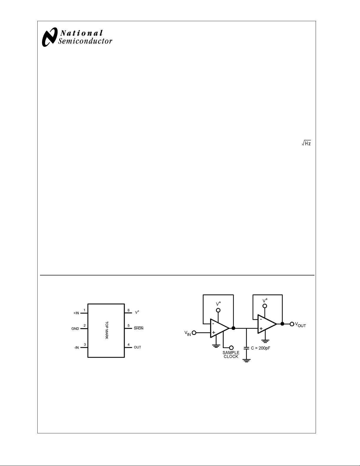
Connection Diagram
SC70-6L
20030441
Top View
Order Number
LMV341MG, LMV341MGX
LMV342MM, LMV342MMX
LMV342MA, LMV342MAX
LMV344MT, LMV344MTX
LMV344MA, LMV344MAX
© 2003 National Semiconductor Corporation DS200304 www.national.com
Sample and Hold Circuit
20030444
Page 2
Absolute Maximum Ratings (Note 1)
If Military/Aerospace specified devices are required,
please contact the National Semiconductor Sales Office/
Distributors for availability and specifications.
Infrared or Convection Reflow
(20 sec.) 235˚C
Wave Soldering Lead Temp.
(10 sec.) 260˚C
ESD Tolerance (Note 2)
Machine Model 200V
Human Body Model 2000V
Differential Input Voltage
LMV341/LMV342/LMV344
Supply Voltage (V
Output Short Circuit to V
Output Short Circuit to V
+-V−
) 5.5V
+
−
Storage Temperature Range −65˚C to 150˚C
Junction Temperature (Note 5) 150˚C
Mounting Temperature
±
Supply Voltage
(Note 3)
(Note 4)
Operating Ratings (Note 1)
Temperature Range −40˚C to 125˚C
Thermal Resistance (θ
6-Pin SC70 414˚C/W
8-Pin SOIC 190˚C/W
8-Pin MSOP 235˚C/W
14-Pin TSSOP 155˚C/W
14-Pin SOIC 145˚C/W
)
JA
2.7V DC Electrical Characteristics (Note 10)
Unless otherwise specified, all limits guaranteed for TJ= 25˚C, V+= 2.7V, V−= 0V, VCM=V+/2, VO=V+/2 and R
Boldface limits apply at the temperature extremes.
Symbol Parameter Conditions
V
OS
Input Offset Voltage LMV341 0.25 4
LMV342/LMV344 0.55 5
TCV
Input Offset Voltage Average
OS
Drift
I
B
I
OS
I
S
Input Bias Current 0.02 120
Input Offset Current 6.6 fA
Supply Current Per Amplifier 100 170
Shutdown Mode, VSD=0V
(LMV341)
CMRR Common Mode Rejection
Ratio
0V ≤ V
0V ≤ V
PSRR Power Supply Rejection Ratio 2.7V ≤ V
V
CM
A
V
Input Common Mode Voltage For CMRR ≥ 50dB 0 −0.2 to 1.9
Large Signal Voltage Gain RL= 10kΩ to 1.35V 78
≤ 1.7V
CM
≤ 1.6V
CM
+
≤ 5V 65
RL=2kΩ to 1.35V 72
V
O
Output Swing RL=2kΩ to 1.35V 24 60
= 10kΩ to 1.35V 5.0 30
R
L
Min
(Note 7)
56
50
60
70
64
60
95
30
40
Typ
(Note 6)
1.7 µV/˚C
45pA 1µA
80 dB
82 dB
(Range)
113
103
26
5.3
>
1MΩ.
L
Max
(Note 7) Units
4.5
mV
5.5
pA
250
µA
230
1.5µA
1.7 V
dB
95
mV
40
www.national.com 2
Page 3
2.7V DC Electrical Characteristics (Note 10) (Continued)
Unless otherwise specified, all limits guaranteed for TJ= 25˚C, V+= 2.7V, V−= 0V, VCM=V+/2, VO=V+/2 and R
Boldface limits apply at the temperature extremes.
Symbol Parameter Conditions
I
O
Output Short Circuit Current Sourcing
Min
(Note 7)
20 32
Typ
(Note 6)
Max
(Note 7) Units
LMV341/LMV342
18 24
LMV344
Sinking 15 24
t
on
V
SD
Turn-on Time from Shutdown (LMV341) 5 µs
Shutdown Pin Voltage Range ON Mode (LMV341) 1.7 to 2.7 2.4 to 2.7
Shutdown Mode (LMV341) 0 to 1 0 to 0.8
2.7V AC Electrical Characteristics (Note 10)
Unless otherwise specified, all limits guaranteed for TJ= 25˚C, V+= 2.7V, V−= 0V, VCM=V+/2, VO=V+/2 and R
Boldface limits apply at the temperature extremes.
Symbol Parameter Conditions Min
(Note 7)
SR Slew Rate R
GBW Gain Bandwidth Product R
Φ
m
G
m
e
n
i
n
Phase Margin RL= 100kΩ 72 deg
Gain Margin RL= 100kΩ 20 dB
Input-Referred Voltage Noise f = 1kHz 40 nV/
Input-Referred Current Noise f = 1kHz 0.001 pA/
= 10kΩ, (Note 9) 1.0 V/µs
L
= 100kΩ,CL= 200pF 1.0 MHz
L
THD Total Harmonic Distortion f = 1kHz, AV=+1
= 600Ω,VIN=1V
R
L
PP
Typ
(Note 6)
Max
(Note 7)
0.017 %
LMV341/LMV342/LMV344
>
1MΩ.
L
mASourcing
V
>
1MΩ.
L
Units
5V DC Electrical Characteristics (Note 10)
Unless otherwise specified, all limits guaranteed for TJ= 25˚C, V+= 5V, V−= 0V, VCM=V+/2, VO=V+/2 and R
Boldface limits apply at the temperature extremes.
Symbol Parameter Conditions
V
OS
Input Offset Voltage LMV341 0.025 4
LMV342/LMV344 0.70 5
TCV
Input Offset Voltage Average
OS
Drift
I
B
I
OS
I
S
Input Bias Current 0.02 200
Input Offset Current 6.6 fA
Supply Current Per Amplifier 107 200
Shutdown Mode, V
(LMV341)
CMRR Common Mode Rejection
Ratio
0V ≤ V
0V ≤ V
PSRR Power Supply Rejection Ratio 2.7V ≤ V
V
CM
Input Common Mode Voltage For CMRR ≥ 50dB 0 −0.2 to 4.2
≤ 4.0V
CM
≤ 3.9V
CM
+
≤ 5V 65
SD
Min
(Note 7)
=0V
56
50
60
Typ
(Note 6)
Max
(Note 7) Units
1.9 µV/˚C
375
260
0.033 1
86 dB
82 dB
(Range)
>
1MΩ.
L
4.5
mV
5.5
pA
µA
µA
1.5
4V
www.national.com3
Page 4
5V DC Electrical Characteristics (Note 10) (Continued)
Unless otherwise specified, all limits guaranteed for TJ= 25˚C, V+= 5V, V−= 0V, VCM=V+/2, VO=V+/2 and R
Boldface limits apply at the temperature extremes.
Symbol Parameter Conditions
A
V
Large Signal Voltage Gain
RL= 10kΩ to 2.5V 78
(Note 8)
RL=2kΩ to 2.5V 72
LMV341/LMV342/LMV344
V
O
I
O
t
on
V
SD
Output Swing RL=2kΩ to 2.5V 32 60
= 10kΩ to 2.5V 7 30
R
L
Output Short Circuit Current Sourcing 85 113
Sinking 50 75
Turn-on Time from Shutdown (LMV341) 5 µs
Shutdown Pin Voltage Range ON Mode (LMV341) 3.1 to 5 4.5 to 5.0
Shutdown Mode (LMV341) 0 to 1 0 to 0.8
Min
(Note 7)
70
64
60
95
30
40
Typ
(Note 6)
116
107
34
7
>
1MΩ.
L
Max
(Note 7) Units
dB
95
40
mV
mV
mA
V
5V AC Electrical Characteristics (Note 10)
Unless otherwise specified, all limits guaranteed for TJ= 25˚C, V+= 5V, V−= 0V, VCM=V+/2, VO=V+/2 and R
Boldface limits apply at the temperature extremes.
Symbol Parameter Conditions Min
(Note 7)
SR Slew Rate R
GBW Gain-Bandwidth Product R
Φ
m
G
m
e
n
i
n
Phase Margin RL= 100kΩ 70 deg
Gain Margin RL= 100kΩ 20 dB
Input-Referred Voltage Noise f = 1kHz 39 nV/
Input-Referred Current Noise f = 1kHz 0.001 pA/
= 10kΩ, (Note 9) 1.0 V/µs
L
= 10kΩ,CL= 200pF 1.0 MHz
L
THD Total Harmonic Distortion f = 1 kHz, AV=+1
= 600Ω,VIN=1V
R
L
Note 1: Absolute Maximum Ratings indicate limits beyond which damage to the device may occur. Operating Ratings indicate conditions for which the device is
intended to be functional, but specific performance is not guaranteed. For guaranteed specifications and the test conditions, see the Electrical Characteristics.
Note 2: Human body model, 1.5kΩ in series with 100pF. Machine model, 0Ω in series with 200pF.
Note 3: Shorting output to V
Note 4: Shorting output to V
Note 5: The maximum power dissipation is a function of T
(T
J(MAX)–TA
Note 6: Typical values represent the most likely parametric norm.
Note 7: All limits are guaranteed by testing or statistical analysis.
Note 8: R
Note 9: Connected as voltage follower with 2V
Note 10: Electrical Table values apply only for factory testing conditions at the temperature indicated. Factory testing conditions result in very limited self-heating
of the device such that T
)/θJA. All numbers apply for packages soldered directly into a PC board.
is connected to mid-supply. The output voltage is GND + 0.2V ≤ VO≤ V+−0.2V
L
+
will adversely affect reliability.
-
will adversely affect reliability.
, θJA, and TA. The maximum allowable power dissipation at any ambient temperature is PD=
J(MAX)
step input. Number specified is the slower of the positive and negative slew rates.
PP
. No guarantee of parametric performance is indicated in the electrical tables under conditions of internal self heating where T
J=TA
PP
Typ
(Note 6)
Max
(Note 7)
0.012 %
>
1MΩ.
L
Units
>
TA.
J
www.national.com 4
Page 5
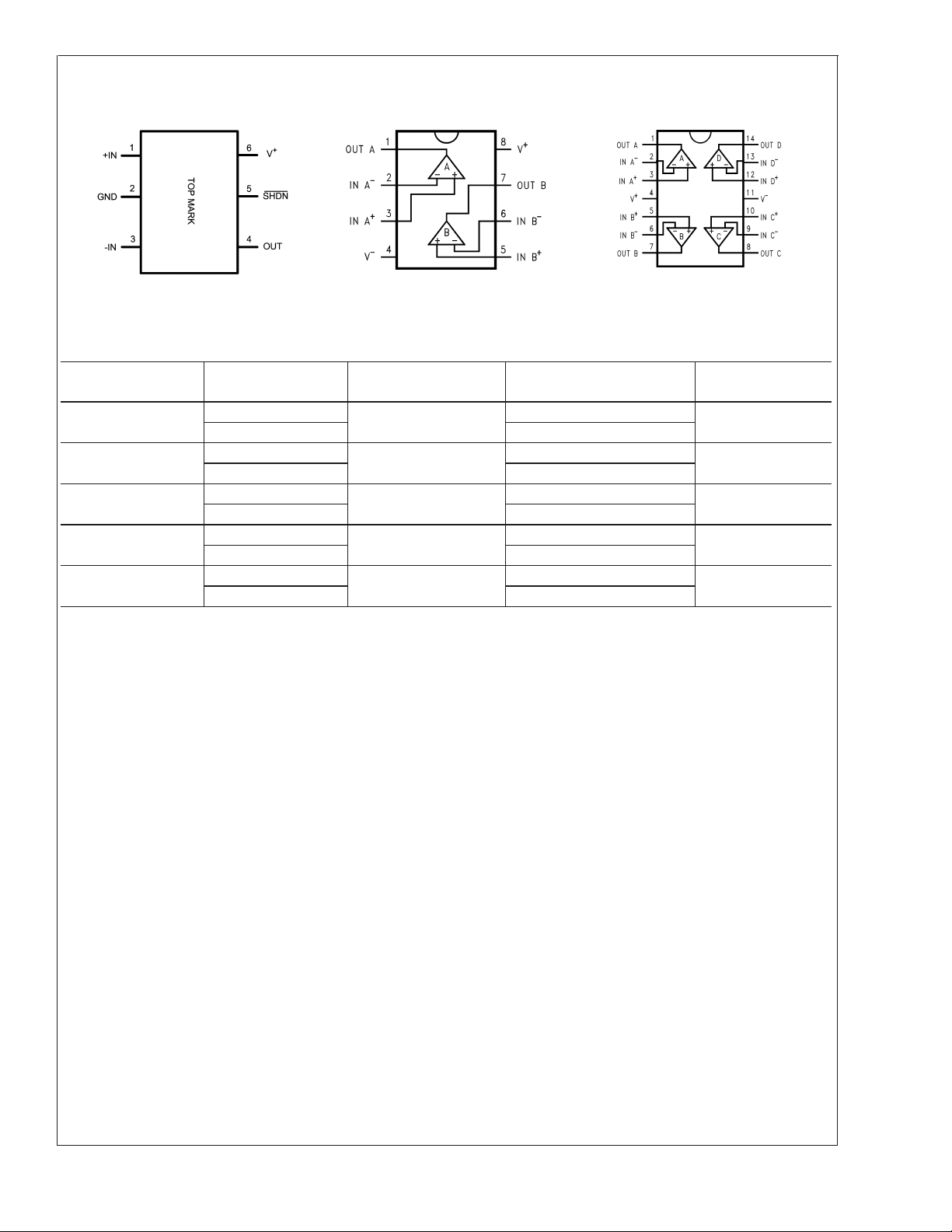
Connection Diagrams
SC70-6L 8-Pin MSOP/SOIC 14-Pin TSSOP/SOIC
LMV341/LMV342/LMV344
20030451
Top View
Top View
20030441
Top View
Ordering Information
Package Part Number Package Marking Transport Media NSC Drawing
6-Pin SC70
8-Pin MSOP
8-Pin SOIC
14-Pin TSSOP
14-Pin SOIC
LMV341MG
LMV341MGX 3k Units Tape and Reel
LMV342MM
LMV342MMX 3.5k Units Tape and Reel
LMV342MA
LMV342MAX 2.5k Units Tape and Reel
LMV344MT
LMV344MTX 2.5k Units Tape and Reel
LMV344MA
LMV344MAX 2.5k Units Tape and Reel
A78
A82A
LMV342MA
LMV344MT
LMV344MA
1k Units Tape and Reel
1k Units Tape and Reel
95 Units/Rail
Rails
55 Units/Rail
20030452
MAA06A
MUA08A
M08A
MTC14
M14A
www.national.com5
Page 6
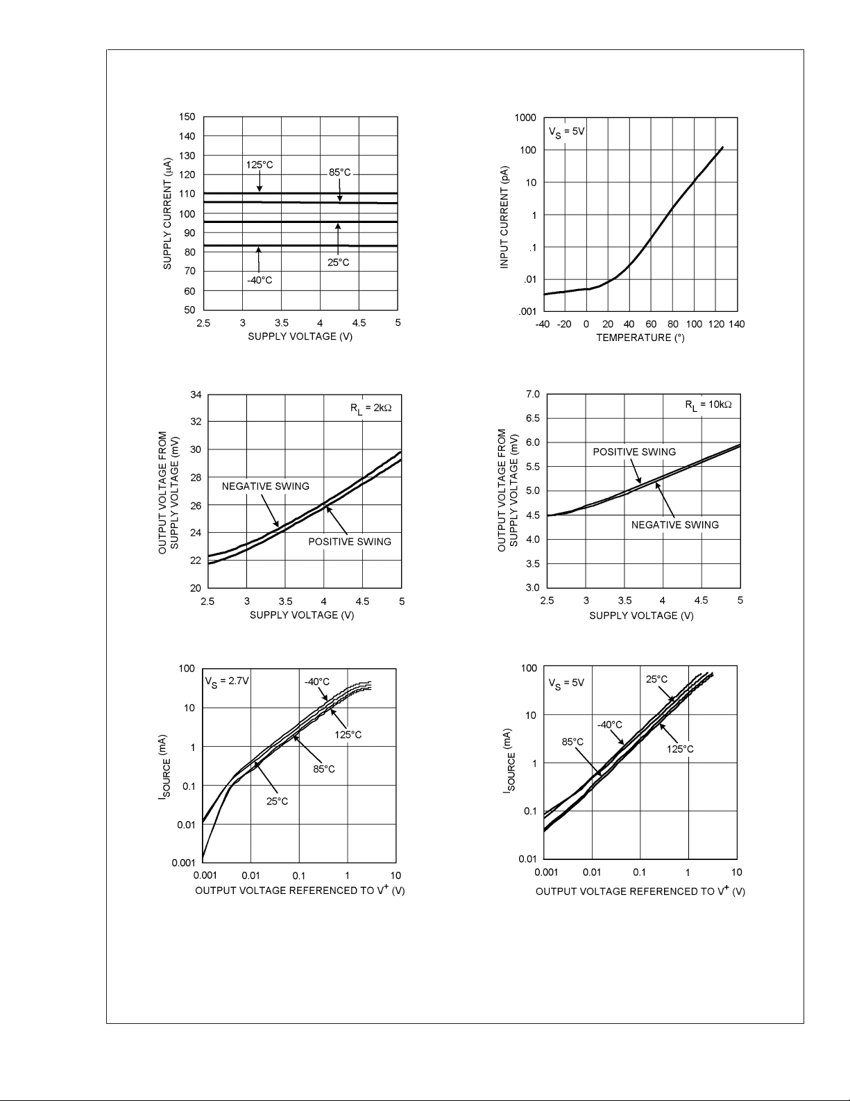
Typical Performance Characteristics
Supply Current vs. Supply Voltage (LMV341) Input Current vs. Temperature
LMV341/LMV342/LMV344
20030428
20030446
Output Voltage Swing vs. Supply Voltage Output Voltage Swing vs. Supply Voltage
20030426 20030427
I
SOURCE
vs. V
OUT
I
SOURCE
vs. V
OUT
20030429
www.national.com 6
20030430
Page 7

Typical Performance Characteristics (Continued)
I
vs. V
SINK
OUT
I
SINK
vs. V
LMV341/LMV342/LMV344
OUT
VOSvs. V
VINvs. V
CM
OUT
20030431
20030433
VOSvs. V
VINvs. V
20030432
CM
20030434
OUT
20030435 20030436
www.national.com7
Page 8

Typical Performance Characteristics (Continued)
CMRR vs. Frequency PSRR vs. Frequency
LMV341/LMV342/LMV344
20030403
Input Voltage Noise vs. frequency Slew Rate vs. V
20030404 20030402
Slew Rate vs. Temperature Slew Rate vs. Temperature
20030401
SUPPLY
20030422 20030423
www.national.com 8
Page 9

Typical Performance Characteristics (Continued)
LMV341/LMV342/LMV344
THD+N vs. Frequency THD+N vs. V
20030425
OUT
Open Loop Frequency Over Temperature Open Loop Frequency Response
20030424
20030421 20030420
Open Loop Frequency Response Gain & Phase vs. C
20030419 20030417
L
www.national.com9
Page 10

Typical Performance Characteristics (Continued)
Gain & Phase vs. C
LMV341/LMV342/LMV344
Stability vs. Capacitive Load Non-Inverting Small Signal Pulse Response
L
20030418
Stability vs. Capacitive Load
20030448
20030405
20030449
Non-Inverting Large Signal Pulse Response Non-Inverting Small Signal Pulse Response
20030408 20030406
www.national.com 10
Page 11

Typical Performance Characteristics (Continued)
Non-Inverting Large Signal Pulse Response Non-Inverting Small Signal Pulse Response
20030409 20030407
Non-Inverting Large Signal Pulse Response Inverting Small Signal Pulse Response
LMV341/LMV342/LMV344
20030410 20030411
Inverting Large Signal Pulse Response Inverting Small Signal Pulse Response
20030414 20030412
www.national.com11
Page 12

Typical Performance Characteristics (Continued)
Inverting Large Signal Pulse Response Inverting Small Signal Pulse Response
LMV341/LMV342/LMV344
20030415 20030413
Inverting Large Signal Pulse Response Crosstalk Rejection vs. Frequency
20030416
20030454
www.national.com 12
Page 13

Application Section
LMV341/342/344
The LMV341/342/344 family of amplifiers features low voltage, low power, and rail-to-rail output operational amplifiers
designed for low voltage portable applications. The family is
designed using all CMOS technology. This results in an ultra
low input bias current. The LMV341 has a shutdown option,
which can be used in portable devices to increase battery
life.
A simplified schematic of the LMV341/342/344 family of
amplifiers is shown in Figure 1. The PMOS input differential
pair allows the input to include ground. The output of this
differential pair is connected to the Class AB turnaround
stage. This Class AB turnaround has a lower quiescent
current, compared to regular turnaround stages. This results
in lower offset, noise, and power dissipation, while slew rate
equals that of a conventional turnaround stage. The output
of the Class AB turnaround stage provides gate voltage to
the complementary common-source transistors at the output
stage. These transistors enable the device to have rail-to-rail
output.
LMV341/LMV342/LMV344
ances, along with the ability of the shutdown pin to be
derived from a separate power source, make LMV341 a
good choice for sample and hold circuits. The sample clock
should be connected to the shutdown pin of the amplifier to
rapidly turn the device on or off.
Figure 2 shows the schematic of a simple sample and hold
circuit. When the sample clock is high the first amplifier is in
normal operation mode and the second amplifier acts as a
buffer. The capacitor, which appears as a load on the first
amplifier, will be charging at this time. The voltage across the
capacitor is that of the non-inverting input of the first amplifier
since it is connected as a voltage-follower. When the sample
clock is low the first amplifier is shut off, bringing the output
impedance to a high value. The high impedance of this
output, along with the very high impedance on the input of
the second amplifier, prevents the capacitor from discharging. There is very little voltage droop while the first amplifier
is in shutdown mode. The second amplifier, which is still in
normal operation mode and is connected as a voltage follower, also provides the voltage sampled on the capacitor at
its output.
20030453
FIGURE 1. Simplified Schematic
CLASS AB TURNAROUND STAGE AMPLIFIER
This patented folded cascode stage has a combined class
AB amplifier stage, which replaces the conventional folded
cascode stage. Therefore, the class AB folded cascode
stage runs at a much lower quiescent current compared to
conventional folded cascode stages. This results in significantly smaller offset and noise contributions. The reduced
offset and noise contributions in turn reduce the offset voltage level and the voltage noise level at the input of the
LMV341/342/344. Also the lower quiescent current results in
a high open-loop gain for the amplifier. The lower quiescent
current does not affect the slew rate of the amplifier nor its
ability to handle the total current swing coming from the input
stage.
The input voltage noise of the device at low frequencies,
below 1kHz, is slightly higher than devices with a BJT input
stage; However the PMOS input stage results in a much
lower input bias current and the input voltage noise drops at
frequencies above 1kHz.
SAMPLE AND HOLD CIRCUIT
The lower input bias current of the LMV341 results in a very
high input impedance. The output impedance when the device is in shutdown mode is quite high. These high imped-
20030444
FIGURE 2. Sample and Hold Circuit
SHUTDOWN FEATURE
The LMV341 is capable of being turned off in order to
conserve power and increase battery life in portable devices.
Once in shutdown mode the supply current is drastically
reduced, 1µA maximum, and the output will be "tri-stated."
The device will be disabled when the shutdown pin voltage is
pulled low. The shutdown pin should never be left unconnected. Leaving the pin floating will result in an undefined
operation mode and the device may oscillate between shutdown and active modes.
The LMV341 typically turns on 2.8µs after the shutdown
voltage is pulled high. The device turns off in less than 400ns
after shutdown voltage is pulled low. Figure 3 and Figure 4
show the turn-on and turn-off time of the LMV341, respectively. In order to reduce the effect of the capacitance added
to the circuit by the scope probe, in the turn-off time circuit a
resistive load of 600Ω is added. Figure 5 and Figure 6 show
the test circuits used to obtain the two plots.
www.national.com13
Page 14

Application Section (Continued)
LMV341/LMV342/LMV344
FIGURE 3. Turn-on Time
20030440
20030443
FIGURE 6. Turn-off Time
LOW INPUT BIAS CURRENT
The LMV341/LMV342/LMV344 Amplifiers have a PMOS input stage. As a result, they will have a much lower input bias
current than devices with BJT input stages. This feature
makes these devices ideal for sensor circuits. A typical curve
of the input bias current of the LMV341 is shown in Figure 7.
FIGURE 4. Turn-off Time
FIGURE 5. Turn-on Time
20030439
20030442
FIGURE 7. Input Bias Current vs. V
20030447
CM
www.national.com 14
Page 15

Physical Dimensions inches (millimeters)
unless otherwise noted
LMV341/LMV342/LMV344
6-Pin SC70
NS Package Number MAA06A
8-Pin MSOP
NS Package Number MUA08A
www.national.com15
Page 16

Physical Dimensions inches (millimeters) unless otherwise noted (Continued)
LMV341/LMV342/LMV344
8-Pin SOIC
NS Package Number M08A
14-Pin TSSOP
NS Package Number MTC14
www.national.com 16
Page 17

Physical Dimensions inches (millimeters) unless otherwise noted (Continued)
14-Pin SOIC
NS Package Number M14A
LMV341/LMV342/LMV344 Single with Shutdown/Dual/Quad General Purpose, 2.7V, Rail-to-Rail
Output, 125˚C, Operational Amplifiers
LIFE SUPPORT POLICY
NATIONAL’S PRODUCTS ARE NOT AUTHORIZED FOR USE AS CRITICAL COMPONENTS IN LIFE SUPPORT
DEVICES OR SYSTEMS WITHOUT THE EXPRESS WRITTEN APPROVAL OF THE PRESIDENT AND GENERAL
COUNSEL OF NATIONAL SEMICONDUCTOR CORPORATION. As used herein:
1. Life support devices or systems are devices or
systems which, (a) are intended for surgical implant
into the body, or (b) support or sustain life, and
whose failure to perform when properly used in
accordance with instructions for use provided in the
2. A critical component is any component of a life
support device or system whose failure to perform
can be reasonably expected to cause the failure of
the life support device or system, or to affect its
safety or effectiveness.
labeling, can be reasonably expected to result in a
significant injury to the user.
National Semiconductor
Americas Customer
Support Center
Email: new.feedback@nsc.com
Tel: 1-800-272-9959
www.national.com
National does not assume any responsibility for use of any circuitry described, no circuit patent licenses are implied and National reserves the right at any time without notice to change said circuitry and specifications.
National Semiconductor
Europe Customer Support Center
Fax: +49 (0) 180-530 85 86
Email: europe.support@nsc.com
Deutsch Tel: +49 (0) 69 9508 6208
English Tel: +44 (0) 870 24 0 2171
Français Tel: +33 (0) 1 41 91 8790
National Semiconductor
Asia Pacific Customer
Support Center
Fax: +65-6250 4466
Email: ap.support@nsc.com
Tel: +65-6254 4466
National Semiconductor
Japan Customer Support Center
Fax: 81-3-5639-7507
Email: jpn.feedback@nsc.com
Tel: 81-3-5639-7560
 Loading...