

Page 1
January 25, 2008
LMV341/LMV342/LMV344
Single with Shutdown/Dual/Quad General Purpose, 2.7V,
Rail-to-Rail Output, 125°C, Operational Amplifiers
General Description
The LMV341/LMV342/LMV344 are single, dual, and quad low
voltage, low power Operational Amplifiers. They are designed
specifically for low voltage portable applications. Other important product characteristics are low input bias current, railto-rail output, and wide temperature range.
The patented class AB turnaround stage significantly reduces
the noise at higher frequencies, power consumption, and offset voltage. The PMOS input stage provides the user with
ultra-low input bias current of 20fA (typical) and high input
impedance.
The industrial-plus temperature range of −40°C to 125°C allows the LMV341/LMV342/LMV344 to accommodate a broad
range of extended environment applications. LMV341 expands National Semiconductor's Silicon Dust™ amplifier portfolio offering enhancements in size, speed, and power
savings. The LMV341/LMV342/LMV344 are guaranteed to
operate over the voltage range of 2.7V to 5.5V and all have
rail-to-rail output.
The LMV341 offers a shutdown pin that can be used to disable
the device. Once in shutdown mode, the supply current is reduced to 45pA (typical). The LMV341/LMV342/LMV344 have
29nV Voltage Noise at 10KHz, 1MHz GBW, 1.0V/μs Slew
Rate, 0.25mVos, and 0.1μA shutdown current (LMV341.)
The LMV341 is offered in the tiny 6-Pin SC70 package, the
LMV342 in space saving 8-Pin MSOP and SOIC, and the
LMV344 in 14-Pin TSSOP and SOIC. These small package
amplifiers offer an ideal solution for applications requiring
minimum PC board footprint. Applications with area con-
strained PC board requirements include portable electronics
such as cellular handsets and PDAs.
Features
(Typical 2.7V supply values; unless otherwise noted)
Guaranteed 2.7V and 5V specifications
■
Input referred voltage noise (@ 10kHz) 29nV/√Hz
■
Supply current (per amplifier)
■
Gain bandwidth product 1.0MHz
■
Slew rate 1.0V/μs
■
Shutdown Current (LMV341) 45pA
■
Turn-on time from shutdown (LMV341)
■
Input bias current 20fA
■
100μA
Applications
Cordless/cellular phones
■
Laptops
■
PDAs
■
PCMCIA/Audio
■
Portable/battery-powered electronic equipment
■
Supply current monitoring
■
Battery monitoring
■
Buffer
■
Filter
■
Driver
■
LMV341/LMV342/LMV344 Single with Shutdown/Dual/Quad General Purpose, 2.7V, Rail-to-Rail
Output, 125°C, Operational Amplifiers
5μs
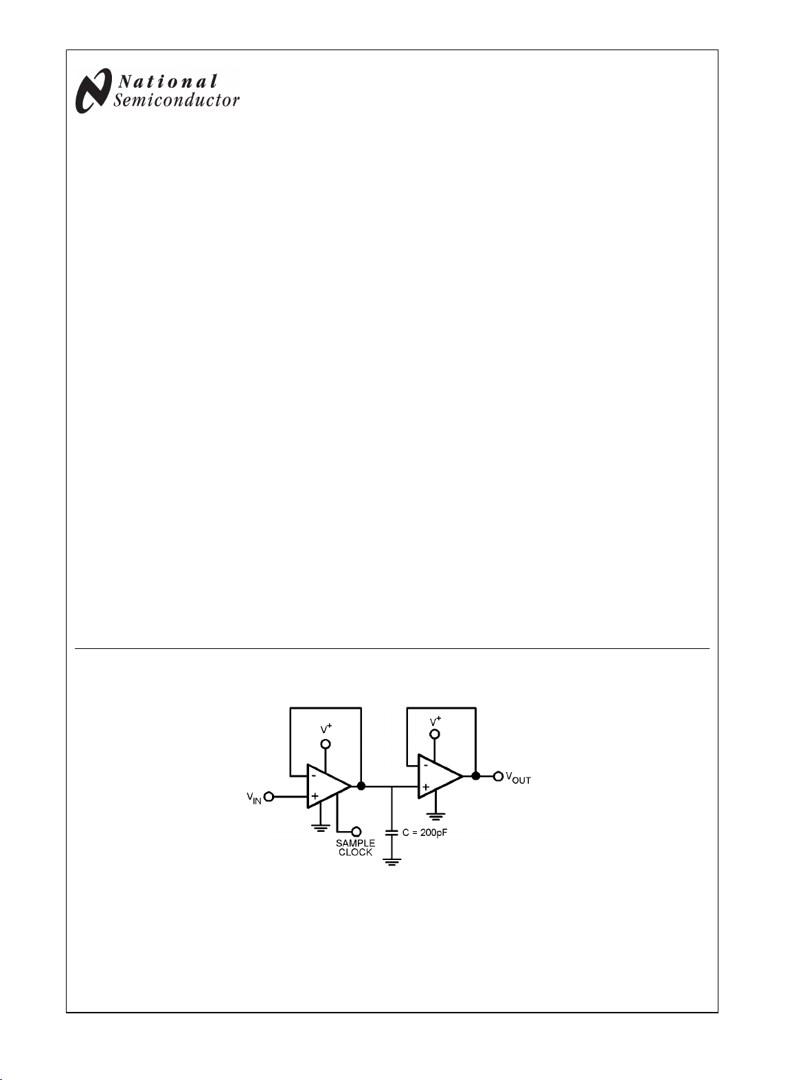
Sample and Hold Circuit
20030444
Silicon Dust™ is a trademark of National Semiconductor Corporation.
© 2008 National Semiconductor Corporation 200304 www.national.com
Page 2
Absolute Maximum Ratings (Note 1)
If Military/Aerospace specified devices are required,
please contact the National Semiconductor Sales Office/
Distributors for availability and specifications.
ESD Tolerance (Note 2)
Machine Model 200V
Human Body Model 2000V
Differential Input Voltage ± Supply Voltage
Supply Voltage (V + -V −)
LMV341/LMV342/LMV344
Output Short Circuit to V
Output Short Circuit to V
Storage Temperature Range −65°C to 150°C
Junction Temperature (Note 5) 150°C
Mounting Temperature
+
−
6.0V
(Note 3)
(Note 4)
Infrared or Convection Reflow
(20 sec.) 235°C
Wave Soldering Lead Temp.
(10 sec.) 260°C
Operating Ratings (Note 1)
Supply Voltage 2.7V to 5.5V
Temperature Range −40°C to 125°C
Thermal Resistance (θ
6-Pin SC70 414°C/W
8-Pin SOIC 190°C/W
8-Pin MSOP 235°C/W
14-Pin TSSOP 155°C/W
14-Pin SOIC 145°C/W
JA
)
2.7V DC Electrical Characteristics (Note 10)
Unless otherwise specified, all limits guaranteed for TJ = 25°C, V+ = 2.7V, V− = 0V, VCM = V+/2, VO = V+/2 and RL > 1MΩ. Boldface
limits apply at the temperature extremes.
Symbol Parameter Conditions Min
(Note 7)
V
OS
Input Offset Voltage LMV341 0.25 4
LMV342/LMV344 0.55 5
TCV
Input Offset Voltage Average
OS
1.7 µV/°C
Drift
I
B
I
OS
I
S
Input Bias Current 0.02 120
Input Offset Current 6.6 fA
Supply Current Per Amplifier 100 170
Shutdown Mode, VSD = 0V
45pA
(LMV341)
CMRR Common Mode Rejection Ratio
0V ≤ VCM ≤ 1.7V
0V ≤ VCM ≤ 1.6V
PSRR Power Supply Rejection Ratio
V
CM
A
V
Input Common Mode Voltage
Large Signal Voltage Gain
2.7V ≤ V+ ≤ 5V
For CMRR ≥ 50dB
RL = 10kΩ to 1.35V
RL = 2kΩ to 1.35V
V
O
Output Swing
RL = 2kΩ to 1.35V
RL = 10kΩ to 1.35V
24 60
5.0 30
56
50
65
60
0 −0.2 to 1.9
78
70
72
64
60
95
30
40
Typ
(Note 6)
Max
(Note 7)
4.5
5.5
250
230
1μA
1.5μA
80 dB
82 dB
1.7 V
(Range)
113
103
95
26
40
5.3
Units
mV
pA
μA
dB
mV
www.national.com 2
Page 3
LMV341/LMV342/LMV344
Symbol Parameter Conditions Min
(Note 7)
I
O
Output Short Circuit Current Sourcing
20 32
Typ
(Note 6)
Max
(Note 7)
LMV341/LMV342
18 24
LMV344
Sinking 15 24
t
on
V
SD
Turn-on Time from Shutdown (LMV341) 5
Shutdown Pin Voltage Range ON Mode (LMV341) 1.7 to 2.7 2.4 to 2.7
Shutdown Mode (LMV341) 0 to 1 0 to 0.8
2.7V AC Electrical Characteristics (Note 10)
Unless otherwise specified, all limits guaranteed for TJ = 25°C, V+ = 2.7V, V− = 0V, VCM = V+/2, VO = V+/2 and RL > 1MΩ.
Boldface limits apply at the temperature extremes.
Symbol Parameter Conditions Min
(Note 7)
SR Slew Rate
GBW Gain Bandwidth Product
Φ
m
G
m
e
n
i
n
Phase Margin
Gain Margin
Input-Referred Voltage Noise f = 1kHz 40
Input-Referred Current Noise f = 1kHz 0.001
RL = 10kΩ, (Note 9)
RL = 100kΩ, CL = 200pF
RL = 100kΩ
RL = 100kΩ
THD Total Harmonic Distortion f = 1kHz, AV = +1
RL = 600Ω, VIN = 1V
PP
1.0
1.0 MHz
72 deg
20 dB
0.017 %
Typ
(Note 6)
Max
(Note 7)
Units
mASourcing
μs
V
Units
V/μs
nV/
pA/
5V DC Electrical Characteristics (Note 10)
Unless otherwise specified, all limits guaranteed for TJ = 25°C, V+ = 5V, V− = 0V, VCM = V+/2, VO = V+/2 and R L > 1MΩ. Bold-
face limits apply at the temperature extremes.
Symbol Parameter Conditions Min
(Note 7)
V
OS
Input Offset Voltage LMV341 0.025 4
LMV342/LMV344 0.70 5
TCV
Input Offset Voltage Average
OS
1.9 µV/°C
Drift
I
B
I
OS
I
S
Input Bias Current 0.02 200
Input Offset Current 6.6 fA
Supply Current Per Amplifier 107 200
Shutdown Mode, VSD = 0V
0.033 1
(LMV341)
CMRR Common Mode Rejection Ratio
0V ≤ VCM ≤ 4.0V
0V ≤ VCM ≤ 3.9V
PSRR Power Supply Rejection Ratio
V
CM
Input Common Mode Voltage
2.7V ≤ V+ ≤ 5V
For CMRR ≥ 50dB
56
50
65
60
0 −0.2 to 4.2
Typ
(Note 6)
Max
(Note 7)
4.5
5.5
375
260
1.5
86 dB
82 dB
4 V
(Range)
Units
mV
pA
μA
μA
3 www.national.com
Page 4
Symbol Parameter Conditions Min
(Note 7)
A
V
Large Signal Voltage Gain (Note
RL = 10kΩ to 2.5V
8)
RL = 2kΩ to 2.5V
78
70
72
Typ
(Note 6)
116
107
Max
(Note 7)
64
V
O
Output Swing
RL = 2kΩ to 2.5V
32 60
95
LMV341/LMV342/LMV344
RL = 10kΩ to 2.5V
60
95
7 30
34
40
30
7
40
I
O
Output Short Circuit Current Sourcing 85 113
Sinking 50 75
t
on
V
SD
Turn-on Time from Shutdown (LMV341) 5 µs
Shutdown Pin Voltage Range ON Mode (LMV341) 3.1 to 5 4.5 to 5.0
Shutdown Mode (LMV341) 0 to 1 0 to 0.8
5V AC Electrical Characteristics (Note 10)
Unless otherwise specified, all limits guaranteed for TJ = 25°C, V+ = 5V, V− = 0V, VCM = V+/2, VO = V+/2 and R L > 1MΩ. Bold-
face limits apply at the temperature extremes.
Symbol Parameter Conditions Min
(Note 7)
SR Slew Rate
GBW Gain-Bandwidth Product
Φ
m
G
m
e
n
i
n
Phase Margin
Gain Margin
Input-Referred Voltage Noise f = 1kHz 39
Input-Referred Current Noise f = 1kHz 0.001
RL = 10kΩ, (Note 9)
RL = 10kΩ, CL = 200pF
RL = 100kΩ
RL = 100kΩ
THD Total Harmonic Distortion f = 1kHz, AV = +1
RL = 600Ω, VIN = 1V
PP
1.0 V/µs
1.0 MHz
70 deg
20 dB
0.012 %
Typ
(Note 6)
Max
(Note 7)
Units
dB
mV
mV
mA
V
Units
nV/
pA/
Note 1: Absolute Maximum Ratings indicate limits beyond which damage to the device may occur. Operating Ratings indicate conditions for which the device is
intended to be functional, but specific performance is not guaranteed. For guaranteed specifications and the test conditions, see the Electrical Characteristics.
Note 2: Human Body Model, applicable std. MIL-STD-883, Method 3015.7. Machine Model, applicable std. JESD22-A115-A (ESD MM std. of JEDEC)
Field-Induced Charge-Device Model, applicable std. JESD22-C101-C (ESD FICDM std. of JEDEC).
Note 3: Shorting output to V+ will adversely affect reliability.
Note 4: Shorting output to V- will adversely affect reliability.
Note 5: The maximum power dissipation is a function of T
is PD = (T
Note 6: Typical values represent the most likely parametric norm as determined at the time of characterization. Actual typical values may vary over time and will
also depend on the application and configuration. The typical values are not tested and are not guaranteed on shipped production material.
Note 7: All limits are guaranteed by testing or statistical analysis.
Note 8: RL is connected to mid-supply. The output voltage is GND + 0.2V ≤ VO ≤ V+ −0.2V
Note 9: Connected as voltage follower with 2VPP step input. Number specified is the slower of the positive and negative slew rates.
Note 10: Electrical Table values apply only for factory testing conditions at the temperature indicated. Factory testing conditions result in very limited self-heating
of the device such that TJ = TA. No guarantee of parametric performance is indicated in the electrical tables under conditions of internal self heating where TJ >
TA.
www.national.com 4
– TA)/ θJA. All numbers apply for packages soldered directly onto a PC Board.
J(MAX)
, θJA. The maximum allowable power dissipation at any ambient temperature
J(MAX)
Page 5
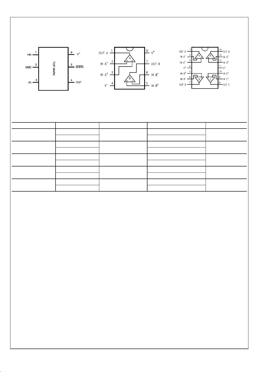
Connection Diagrams
LMV341/LMV342/LMV344
6-Pin SC70
Top View
20030441
8-Pin MSOP/SOIC
Top View
20030451
14-Pin TSSOP/SOIC
Top View
Ordering Information
Package Part Number Package Marking Transport Media NSC Drawing
6-Pin SC70
8-Pin MSOP
8-Pin SOIC
14-Pin TSSOP
14-Pin SOIC
LMV341MG
LMV341MGX 3k Units Tape and Reel
LMV342MM
LMV342MMX 3.5k Units Tape and Reel
LMV342MA
LMV342MAX 2.5k Units Tape and Reel
LMV344MT
LMV344MTX 2.5k Units Tape and Reel
LMV344MA
LMV344MAX 2.5k Units Tape and Reel
A78
A82A
LMV342MA
LMV344MT
LMV344MA
1k Units Tape and Reel
1k Units Tape and Reel
95 Units/Rail
Rails
55 Units/Rail
20030452
MAA06A
MUA08A
M08A
MTC14
M14A
5 www.national.com
Page 6
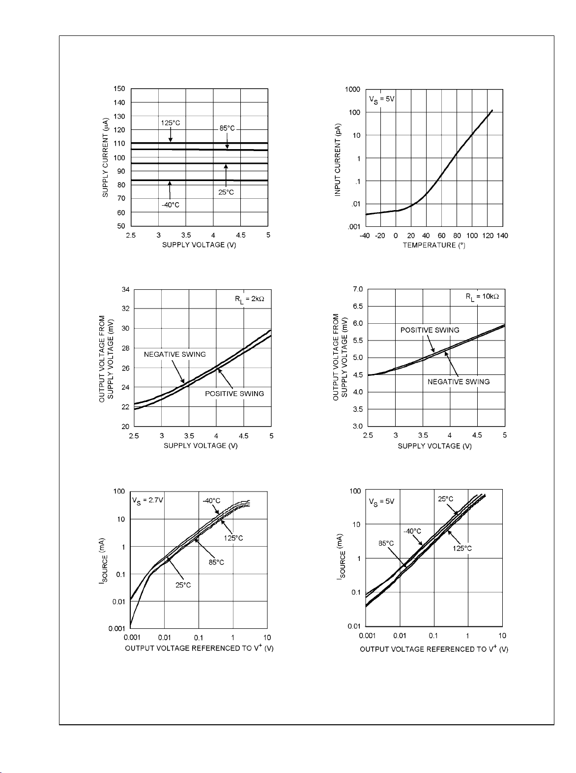
Typical Performance Characteristics
Supply Current vs. Supply Voltage (LMV341)
LMV341/LMV342/LMV344
Output Voltage Swing vs. Supply Voltage
20030428
Input Current vs. Temperature
20030446
Output Voltage Swing vs. Supply Voltage
20030426
I
vs. V
SOURCE
www.national.com 6
OUT
20030429
I
SOURCE
vs. V
20030427
OUT
20030430
Page 7

I
SINK
vs. V
OUT
I
SINK
vs. V
LMV341/LMV342/LMV344
OUT
VOS vs. V
VIN vs. V
CM
OUT
20030431
20030433
VOS vs. V
VIN vs. V
20030432
CM
20030434
OUT
20030435
20030436
7 www.national.com
Page 8

CMRR vs. Frequency
LMV341/LMV342/LMV344
PSRR vs. Frequency
Input Voltage Noise vs. frequency
Slew Rate vs. Temperature
20030403
20030404
Slew Rate vs. V
SUPPLY
Slew Rate vs. Temperature
20030401
20030402
20030422
www.national.com 8
20030423
Page 9

LMV341/LMV342/LMV344
THD+N vs. Frequency
20030425
Open Loop Frequency Over Temperature
THD+N vs. V
OUT
Open Loop Frequency Response
20030424
Open Loop Frequency Response
20030421
20030419
Gain and Phase vs. C
20030420
L
20030417
9 www.national.com
Page 10

Gain and Phase vs. C
LMV341/LMV342/LMV344
L
Stability vs. Capacitive Load
20030418
Stability vs. Capacitive Load
20030449
Non-Inverting Large Signal Pulse Response
20030448
Non-Inverting Small Signal Pulse Response
20030405
Non-Inverting Small Signal Pulse Response
20030408
www.national.com 10
20030406
Page 11

LMV341/LMV342/LMV344
Non-Inverting Large Signal Pulse Response
20030409
Non-Inverting Large Signal Pulse Response
Non-Inverting Small Signal Pulse Response
20030407
Inverting Small Signal Pulse Response
20030410
Inverting Large Signal Pulse Response
20030414
20030411
Inverting Small Signal Pulse Response
20030412
11 www.national.com
Page 12

Inverting Large Signal Pulse Response
LMV341/LMV342/LMV344
Inverting Small Signal Pulse Response
20030415
Inverting Large Signal Pulse Response
20030416
20030413
Crosstalk Rejection vs. Frequency
20030454
www.national.com 12
Page 13

Application Section
LMV341/LMV342/LMV344
The LMV341/LMV342/LMV344 family of amplifiers features
low voltage, low power, and rail-to-rail output operational amplifiers designed for low voltage portable applications. The
family is designed using all CMOS technology. This results in
an ultra low input bias current. The LMV341 has a shutdown
option, which can be used in portable devices to increase
battery life.
A simplified schematic of the LMV341/LMV342/LMV344 family of amplifiers is shown in Figure 1. The PMOS input differ-
ential pair allows the input to include ground. The output of
this differential pair is connected to the Class AB turnaround
stage. This Class AB turnaround has a lower quiescent current, compared to regular turnaround stages. This results in
lower offset, noise, and power dissipation, while slew rate
equals that of a conventional turnaround stage. The output of
the Class AB turnaround stage provides gate voltage to the
complementary common-source transistors at the output
stage. These transistors enable the device to have rail-to-rail
output.
LMV341/LMV342/LMV344
SAMPLE AND HOLD CIRCUIT
The lower input bias current of the LMV341 results in a very
high input impedance. The output impedance when the device is in shutdown mode is quite high. These high
impedances, along with the ability of the shutdown pin to be
derived from a separate power source, make LMV341 a good
choice for sample and hold circuits. The sample clock should
be connected to the shutdown pin of the amplifier to rapidly
turn the device on or off.
Figure 2 shows the schematic of a simple sample and hold
circuit. When the sample clock is high the first amplifier is in
normal operation mode and the second amplifier acts as a
buffer. The capacitor, which appears as a load on the first
amplifier, will be charging at this time. The voltage across the
capacitor is that of the non-inverting input of the first amplifier
since it is connected as a voltage-follower. When the sample
clock is low the first amplifier is shut off, bringing the output
impedance to a high value. The high impedance of this output,
along with the very high impedance on the input of the second
amplifier, prevents the capacitor from discharging. There is
very little voltage droop while the first amplifier is in shutdown
mode. The second amplifier, which is still in normal operation
mode and is connected as a voltage follower, also provides
the voltage sampled on the capacitor at its output.
20030453
FIGURE 1. Simplified Schematic
CLASS AB TURNAROUND STAGE AMPLIFIER
This patented folded cascode stage has a combined class AB
amplifier stage, which replaces the conventional folded cascode stage. Therefore, the class AB folded cascode stage
runs at a much lower quiescent current compared to conventional folded cascode stages. This results in significantly
smaller offset and noise contributions. The reduced offset and
noise contributions in turn reduce the offset voltage level and
the voltage noise level at the input of the LMV341/LMV342/
LMV344. Also the lower quiescent current results in a high
open-loop gain for the amplifier. The lower quiescent current
does not affect the slew rate of the amplifier nor its ability to
handle the total current swing coming from the input stage.
The input voltage noise of the device at low frequencies, below 1kHz, is slightly higher than devices with a BJT input
stage; However the PMOS input stage results in a much lower
input bias current and the input voltage noise drops at frequencies above 1kHz.
20030444
FIGURE 2. Sample and Hold Circuit
SHUTDOWN FEATURE
The LMV341 is capable of being turned off in order to conserve power and increase battery life in portable devices.
Once in shutdown mode the supply current is drastically reduced, 1µA maximum, and the output will be "tri-stated."
The device will be disabled when the shutdown pin voltage is
pulled low. The shutdown pin should never be left unconnected. Leaving the pin floating will result in an undefined operation mode and the device may oscillate between shutdown
and active modes.
The LMV341 typically turns on 2.8µs after the shutdown voltage is pulled high. The device turns off in less than 400ns after
shutdown voltage is pulled low. Figure 3 and Figure 4 show
the turn-on and turn-off time of the LMV341, respectively. In
order to reduce the effect of the capacitance added to the
circuit by the scope probe, in the turn-off time circuit a resistive
load of 600Ω is added. Figure 5 and Figure 6 show the test
circuits used to obtain the two plots.
13 www.national.com
Page 14

LMV341/LMV342/LMV344
20030443
FIGURE 6. Turn-off Time
FIGURE 3. Turn-on Time
FIGURE 4. Turn-off Time
20030440
20030439
LOW INPUT BIAS CURRENT
The LMV341/LMV342/LMV344 Amplifiers have a PMOS input stage. As a result, they will have a much lower input bias
current than devices with BJT input stages. This feature
makes these devices ideal for sensor circuits. A typical curve
of the input bias current of the LMV341 is shown in Figure 7.
20030447
FIGURE 7. Input Bias Current vs. V
CM
20030442
FIGURE 5. Turn-on Time
www.national.com 14
Page 15

Physical Dimensions inches (millimeters) unless otherwise noted
LMV341/LMV342/LMV344
NS Package Number MAA06A
NS Package Number MUA08A
6-Pin SC70
8-Pin MSOP
15 www.national.com
Page 16

LMV341/LMV342/LMV344
NS Package Number M08A
NS Package Number MTC14
8-Pin SOIC
14-Pin TSSOP
www.national.com 16
Page 17

LMV341/LMV342/LMV344
NS Package Number M14A
14-Pin SOIC
17 www.national.com
Page 18

Notes
For more National Semiconductor product information and proven design tools, visit the following Web sites at:
Products Design Support
Amplifiers www.national.com/amplifiers WEBENCH www.national.com/webench
Audio www.national.com/audio Analog University www.national.com/AU
Clock Conditioners www.national.com/timing App Notes www.national.com/appnotes
Data Converters www.national.com/adc Distributors www.national.com/contacts
Displays www.national.com/displays Green Compliance www.national.com/quality/green
Ethernet www.national.com/ethernet Packaging www.national.com/packaging
Interface www.national.com/interface Quality and Reliability www.national.com/quality
LVDS www.national.com/lvds Reference Designs www.national.com/refdesigns
Power Management www.national.com/power Feedback www.national.com/feedback
Switching Regulators www.national.com/switchers
LDOs www.national.com/ldo
LED Lighting www.national.com/led
Output, 125°C, Operational Amplifiers
PowerWise www.national.com/powerwise
Serial Digital Interface (SDI) www.national.com/sdi
Temperature Sensors www.national.com/tempsensors
Wireless (PLL/VCO) www.national.com/wireless
THE CONTENTS OF THIS DOCUMENT ARE PROVIDED IN CONNECTION WITH NATIONAL SEMICONDUCTOR CORPORATION
(“NATIONAL”) PRODUCTS. NATIONAL MAKES NO REPRESENTATIONS OR WARRANTIES WITH RESPECT TO THE ACCURACY
OR COMPLETENESS OF THE CONTENTS OF THIS PUBLICATION AND RESERVES THE RIGHT TO MAKE CHANGES TO
SPECIFICATIONS AND PRODUCT DESCRIPTIONS AT ANY TIME WITHOUT NOTICE. NO LICENSE, WHETHER EXPRESS,
IMPLIED, ARISING BY ESTOPPEL OR OTHERWISE, TO ANY INTELLECTUAL PROPERTY RIGHTS IS GRANTED BY THIS
DOCUMENT.
TESTING AND OTHER QUALITY CONTROLS ARE USED TO THE EXTENT NATIONAL DEEMS NECESSARY TO SUPPORT
NATIONAL’S PRODUCT WARRANTY. EXCEPT WHERE MANDATED BY GOVERNMENT REQUIREMENTS, TESTING OF ALL
PARAMETERS OF EACH PRODUCT IS NOT NECESSARILY PERFORMED. NATIONAL ASSUMES NO LIABILITY FOR
APPLICATIONS ASSISTANCE OR BUYER PRODUCT DESIGN. BUYERS ARE RESPONSIBLE FOR THEIR PRODUCTS AND
APPLICATIONS USING NATIONAL COMPONENTS. PRIOR TO USING OR DISTRIBUTING ANY PRODUCTS THAT INCLUDE
NATIONAL COMPONENTS, BUYERS SHOULD PROVIDE ADEQUATE DESIGN, TESTING AND OPERATING SAFEGUARDS.
EXCEPT AS PROVIDED IN NATIONAL’S TERMS AND CONDITIONS OF SALE FOR SUCH PRODUCTS, NATIONAL ASSUMES NO
LIABILITY WHATSOEVER, AND NATIONAL DISCLAIMS ANY EXPRESS OR IMPLIED WARRANTY RELATING TO THE SALE
AND/OR USE OF NATIONAL PRODUCTS INCLUDING LIABILITY OR WARRANTIES RELATING TO FITNESS FOR A PARTICULAR
PURPOSE, MERCHANTABILITY, OR INFRINGEMENT OF ANY PATENT, COPYRIGHT OR OTHER INTELLECTUAL PROPERTY
RIGHT.
LIFE SUPPORT POLICY
NATIONAL’S PRODUCTS ARE NOT AUTHORIZED FOR USE AS CRITICAL COMPONENTS IN LIFE SUPPORT DEVICES OR
SYSTEMS WITHOUT THE EXPRESS PRIOR WRITTEN APPROVAL OF THE CHIEF EXECUTIVE OFFICER AND GENERAL
COUNSEL OF NATIONAL SEMICONDUCTOR CORPORATION. As used herein:
Life support devices or systems are devices which (a) are intended for surgical implant into the body, or (b) support or sustain life and
whose failure to perform when properly used in accordance with instructions for use provided in the labeling can be reasonably expected
to result in a significant injury to the user. A critical component is any component in a life support device or system whose failure to perform
can be reasonably expected to cause the failure of the life support device or system or to affect its safety or effectiveness.
National Semiconductor and the National Semiconductor logo are registered trademarks of National Semiconductor Corporation. All other
brand or product names may be trademarks or registered trademarks of their respective holders.
Copyright© 2008 National Semiconductor Corporation
For the most current product information visit us at www.national.com
National Semiconductor
Americas Technical
Support Center
Email:
new.feedback@nsc.com
LMV341/LMV342/LMV344 Single with Shutdown/Dual/Quad General Purpose, 2.7V, Rail-to-Rail
www.national.com
Tel: 1-800-272-9959
National Semiconductor Europe
Technical Support Center
Email: europe.support@nsc.com
German Tel: +49 (0) 180 5010 771
English Tel: +44 (0) 870 850 4288
National Semiconductor Asia
Pacific Technical Support Center
Email: ap.support@nsc.com
National Semiconductor Japan
Technical Support Center
Email: jpn.feedback@nsc.com
 Loading...