

Page 1
August 1999
LMV331 Single / LMV393 Dual / LMV339 Quad
General Purpose, Low Voltage, TinyPack Comparators
LMV331 Single / LMV393 Dual / LMV339 Quad General Purpose, Low Voltage, TinyPack
Comparators
General Description
The LMV393 and LMV339 are low voltage (2.7-5V) versions
of the dual and quad comparators, LM393/339, which are
specified at 5-30V. The LMV331 is the single version, which
is availableinspace saving SC70-5 and SOT23-5 packages.
SC70-5 is approximately half the size of SOT23-5.
The LMV393 is available in 8-pin SOICand 8-pin MSOP.The
LMV339 is available in 14-pin SOIC and 14-pin TSSOP.
The LMV331/393/339 is the most cost-effective solution
where space, low voltage, low power and price are the primary specification in circuit design for portable consumer
products. They offer specifications that meet or exceed the
familiar LM393/339 at a fraction of the supply current.
The chips are built with National’s advanced Submicron
Silicon-Gate BiCMOS process. The LMV331/393/339 have
bipolar input and output stages for improved noise performance.
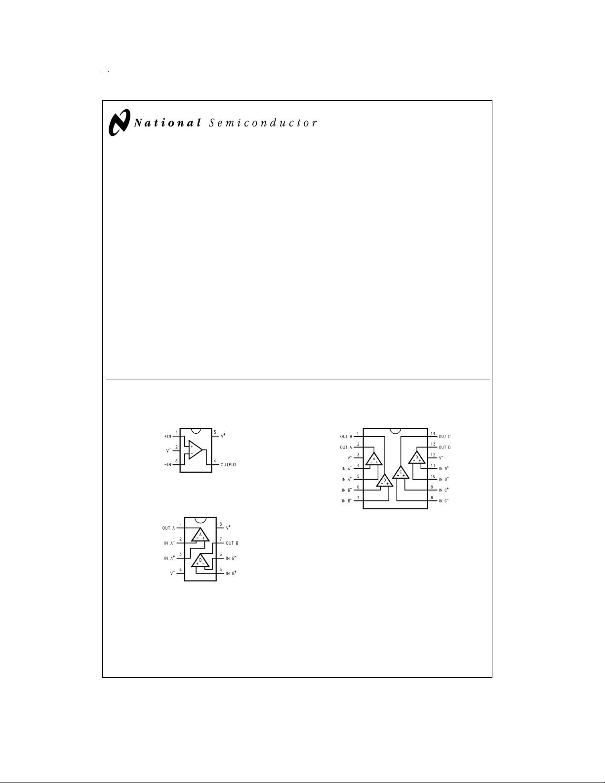
Connection Diagrams
5-Pin SC70-5/SOT23-5
DS100080-1
Top View
Features
(For 5V Supply, Typical Unless Otherwise Noted)
n Space Saving SC70-5 Package (2.0 x 2.1 x 1.0
mm)
n Space Saving SOT23-5 Package (3.00 x 3.01 x
1.43 mm)
n Guaranteed 2.7V and 5V Performance
n Industrial Temperature Range −40˚C to +85˚C
n Low Supply Current 60µA/Channel
n Input Common Mode Voltage Range Includes Ground
n Low Output Saturation Voltage 200 mV
Applications
n Mobile Communications
n Notebooks and PDA’s
n Battery Powered Electronics
n General Purpose Portable Device
n General Purpose Low Voltage Applications
14-Pin SO/TSSOP
8-Pin SO/MSOP
Top View
DS100080-2
Top View
© 1999 National Semiconductor Corporation DS100080 www.national.com
DS100080-3
Page 2
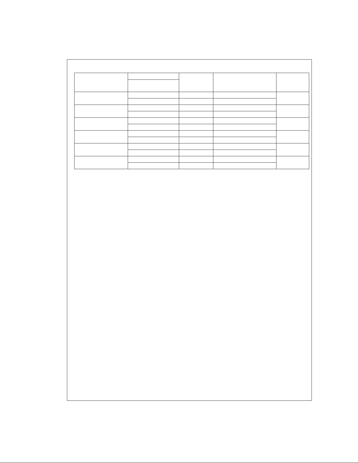
Ordering Information
Temperature Range Packaging
Package
5-pin SC70-5 LMV331M7 C13 1k Units Tape and Reel MAA05
5-pin SOT23-5 LMV331M5 C12 1k Units Tape and Reel MA05B
8-pin Small Outline LMV393M LMV393M Rails
8-pin MSOP LMV393MM LMV393 1k UnitsTape and Reel
14-pin Small Outline LMV339M LMV339M Rails
14-pin TSSOP LMV339MT LMV339MT Rails
Industrial
−40˚C to +85˚C
LMV331M7X C13 3k Units Tape and Reel
LMV331M5X C12 3k Units Tape and Reel
LMV393MX LMV393M 2.5k Units Tape and Reel
LMV393MMX LMV393 3.5k Units Tape and Reel
LMV339MX LMV339M 2.5k Units Tape and Reel
LMV339MTX LMV339MT 2.5k Units Tape and Reel
Marking
Transport
Media
NSC
Drawing
M08A
MUA08A
M14A
MTC14
www.national.com 2
Page 3
Absolute Maximum Ratings (Note 1)
If Military/Aerospace specified devices are required,
please contact the National Semiconductor Sales Office/
Distributors for availability and specifications.
ESD Tolerance (Note 2)
Human Body Model
LMV331/ 393/ 339 800V
Machine Model LMV331/339/393 120V
Differential Input Voltage
Voltage on any pin
(referred to V
−
pin)
Soldering Information
Infrared or Convection (20 sec) 235˚C
Storage Temp. Range −65˚C to +150˚C
Junction Temperature (Note 3) 150˚C
±
Supply Voltage
5.5V
Operating Ratings(Note 1)
Supply Voltage 2.7V to 5.0V
Temperature Range
LMV393, LMV339,
LMV331
Thermal Resistance (θ
M Package, 8-pin Surface
Mount
M Package, 14-pin Surface
Mount
MTC Package, 14-pin
TSSOP
MAA05 Package, 5-pin
SC70-5
M05A Package 5 -pin
SOT23-5
MM Package, 8-pin Mini
)
JA
−40˚C ≤ T
≤ +85˚C
J
190˚C/W
145˚C/W
155˚C/W
478˚C/W
265˚C/W
235˚C/W
Surface Mount
2.7V DC Electrical Characteristics
Unless otherwise specified, all limits guaranteed for TJ= 25˚C, V+=2.7V, V−=0V. Boldface limits apply at the temperature
extremes.
Symbol Parameter Conditions Typ
V
OS
TCV
I
B
I
OS
V
CM
Input Offset Voltage
Input Offset Voltage
OS
Average Drift
Input Bias Current
Input Offset Current
Input Voltage Range −0.1 V
(Note 4)
1.7 7
2.0 V
V
SAT
I
O
I
S
Saturation Voltage I
≤ 1mA 200 mV
sink
Output Sink Current VO≤ 1.5V 23 5 mA min
Supply Current LMV331 40 100 µA max
LMV393
Both Comparators
LMV339
140 200 µA max
All four Comparators
Output Leakage Current .003 1 µA max
LMV331/
393/339
Limit
(Note 5)
5 µV/˚C
10
5
250
400
50
150
70 140 µA max
Units
nA max
nA max
mV
max
2.7V AC Electrical Characteristics
TJ= 25˚C, V+=2.7V, R
Symbol Parameter Conditions Typ
t
PHL
t
PLH
Propagation Delay (High to Low) Input Overdrive=10 mV 1000 ns
Propagation Delay (Low to High) Input Overdrive=10 mV 500 ns
=
5.1 kΩ,V−=0V.
L
(Note 4)
Input Overdrive=100 mV 350 ns
Input Overdrive=100 mV 400 ns
Units
www.national.com3
Page 4
5V DC Electrical Characteristics
Unless otherwise specified, all limits guaranteed for TJ= 25˚C, V+=5V, V−=0V. Boldface limits apply at the temperature
extremes.
Symbol Parameter Conditions Typ
V
OS
TCV
I
B
I
OS
V
CM
Input Offset Voltage 1.7 7
Input Offset Voltage
OS
Average Drift
Input Bias Current
Input Offset Current
Input Voltage Range −0.1 V
(Note 4)
4.2 V
A
V
V
sat
I
O
I
S
Voltage Gain 50 20 V/mV min
Saturation Voltage I
≤ 4 mA 200 400
sink
Output Sink Current VO≤ 1.5V 84 10 mA
Supply Current LMV331 60 120
LMV393
100 200
Both Comparators
LMV339
170 300
All four Comparators
Output Leakage Current .003 1 µA max
5 µV/˚C
25
2
LMV331/
393/339
Limit
(Note 5)
9
250
400
50
150
700
150
250
350
Units
mV
max
nA max
nA max
mV
max
µA max
µA max
µA max
5V AC Electrical Characteristics
TJ= 25˚C, V+=5V, R
Symbol Parameter Conditions Typ
t
PHL
t
PLH
Note 1: Absolute Maximum Ratings indicate limits beyond which damage to the device may occur. Operating Ratings indicate conditions for which the device is intended to be functional, but specific performance is not guaranteed. For guaranteed specifications and the test conditions, see the Electrical characteristics.
Note 2: : Human body model, 1.5kΩ in series with 100 pF. Machine model, 200Ω in series with 100 pF.
Note 3: The maximum power dissipation is a functionof T
-TA)/θJA. All numbers apply for packages soldered directly into a PC board.
Note 4: Typical Values represent the most likely parametric norm.
Note 5: All limits are guaranteed by testing or statistical analysis.
www.national.com 4
Propagation Delay (High to Low) Input Overdrive=10 mV 600 ns
Propagation Delay (Low to High) Input Overdrive=10 mV 450 ns
=
5.1 kΩ,V−=0V.
L
(Note 4)
Input Overdrive=100 mV 200 ns
Input Overdrive=100 mV 300 ns
, θJA, and TA. The maximum allowable power dissipation at any ambient temperature is P
J(max)
D
Units
=
(T
J(max)
Page 5
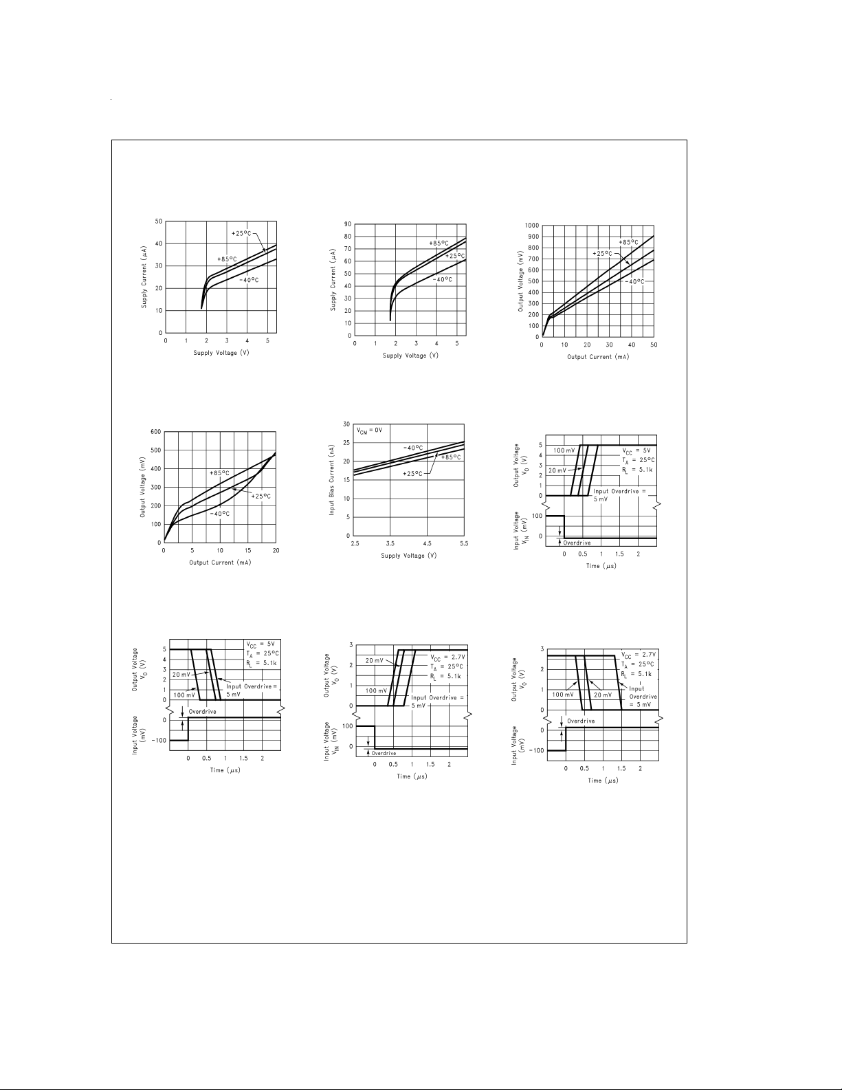
Typical Performance Characteristics Unless otherwise specified, V
Supply Current vs
Supply Voltage Output High
(LMV331)
Supply Current vs
Supply Voltage Output Low
(LMV331)
Output Voltage vs
Output Current at 5V Supply
=
+5V, single supply, T
S
=
25˚C
A
Output Voltage vs
Output Current
at 2.7 Supply
Response Time for
Input Overdrive
Positive Transition
DS100080-34
DS100080-38
Input Bias Current vs
Supply Voltage
Response Time vs
Input Overdrives
Negative Transition
DS100080-33
DS100080-36
DS100080-37
Response Time vs
Input Overdrives
Negative Transition
DS100080-42
Response Time for
Input Overdrive
Positive Transition
DS100080-43
DS100080-41
DS100080-40
www.national.com5
Page 6
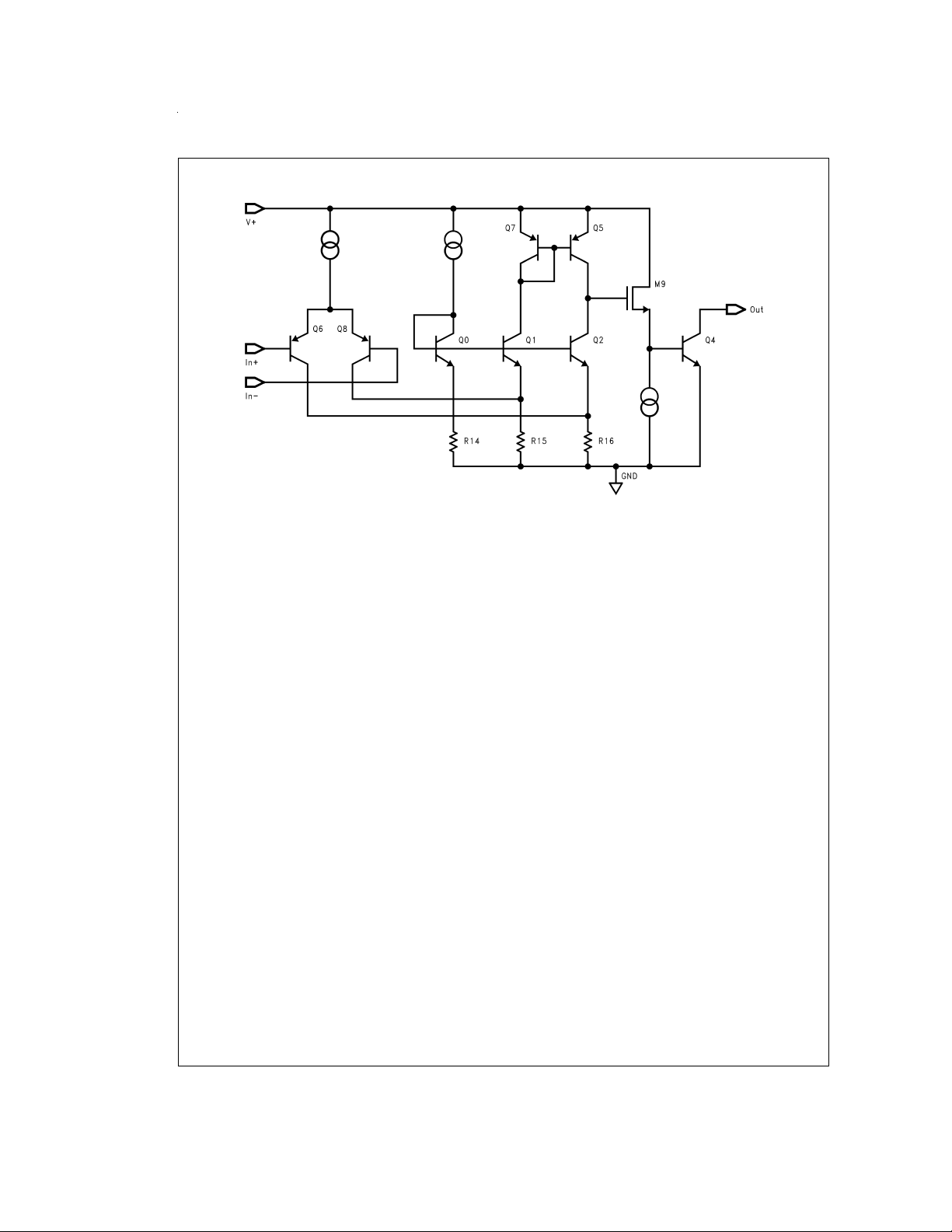
Simplified Schematic
DS100080-47
www.national.com 6
Page 7
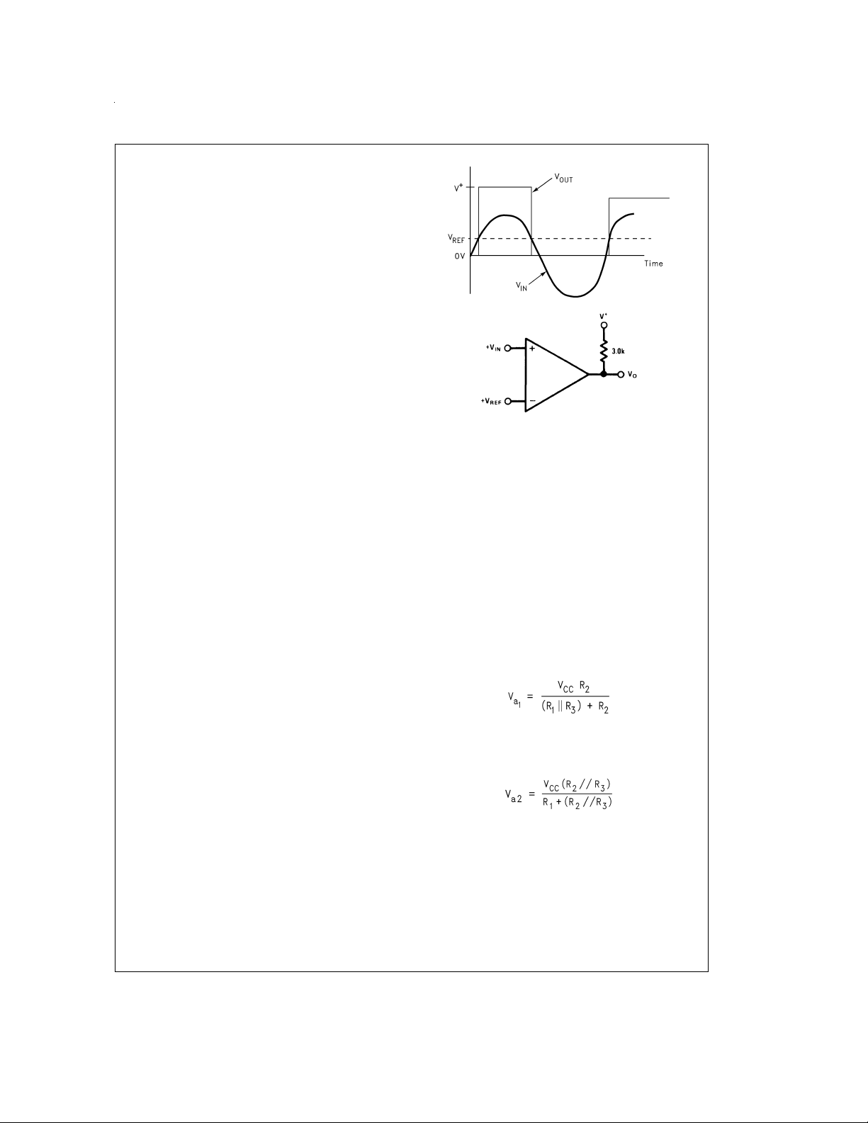
Application Circuits
Basic Comparator
A basic comparator circuit is used for converting analog signals to a digital output. The LMV331/393/339 have an
open-collector output stage, which requires a pull-up resistor
to a positive supply voltage for the output to switch properly.
When the internal output transistor is off, the output voltage
will be pulled up to the external positive voltage.
The output pull-up resistor should be chosen high enough so
as to avoid excessive power dissipation yet low enough to
supply enough drive to switch whatever load circuitry is used
on the comparator output. On the LMV331/393/339 the
pull-up resistor should range between 1k to 10kΩ.
The comparator compares the input voltage (V
non-inverting pin to the reference voltage (V
ing pin. If V
saturation voltage. On the other hand, if V
V
ref
is less than V
in
, the output voltage (Vo)isatthe
ref
, the output voltage (Vo)isatV
.
cc.
)atthe
in
) at the invert-
ref
is greater than
in
DS100080-26
DS100080-4
FIGURE 1. Basic Comparator
Comparator with Hysteresis
The basic comparator configuration may oscillate or produce
a noisy output if the applied differential input voltage is near
the comparator’s offset voltage. This usually happens when
the input signal is moving very slowly across the comparator’s switching threshold. This problem can be prevented by
the addition of hysteresis or positive feedback.
Inverting Comparator with Hysteresis
The inverting comparator with hysteresis requires a three resistor network that are referenced to the supply voltage V
of the comparator. When Vin at the inverting input is less
than V
, the voltage at the non-inverting node of the com-
a
parator (V
assume V
sistors can be represented as R
lower input trip voltage V
<
Va), the output voltage is high (for simplicity
in
switches as high as Vcc). The three network re-
o
//R3in series with R2. The
1
is defined as
a1
cc
When Vinis greater than Va (VinVa), the output voltage is
low very close to ground. In this case the three network resistors can be presented as R
per trip voltage V
is defined as
a2
//R3in series with R1. The up-
2
The total hysteresis provided by the network is defined as
=
∆V
V
a
a1-Va2
To assure that the comparator will always switch fully to V
and not be pulled down by the load the resistors values
should be chosen as follow:
<<
R
pull-up
and R
R
load
>
R
pull-up
.
www.national.com7
1
cc
Page 8

Application Circuits (Continued)
FIGURE 2. Inverting Comparator with Hysteresis
Non-Inverting Comparator with Hysteresis
Non inverting comparator with hysteresis requires a two resistor network, and a voltage reference (V
input. When V
to switch from low to high, V
is calculated by
is low, the output is also low. For the output
in
must rise up to V
in
) at the inverting
ref
where V
in1
in1
When Vinis high, the output is also high, to make the comparator switch back to it’s low state, V
fore V
will again equal V
a
ref.Vin
The hysteresis of this circuit is the difference between V
and V
.
in2
www.national.com 8
∆V
in=VccR1/R2
must equal V
in
can be calculated by:
be-
ref
in1
DS100080-25
DS100080-22
DS100080-23
Page 9

Application Circuits (Continued)
Square Wave Oscillator
Comparators are ideal for oscillator applications. Thissquare
wave generator uses the minimum number of components.
The output frequency is set by the RC time constant of the
capacitor C
The maximum frequency is limited only by the large signal
propagation delay of the comparator in addition to any capacitive loading at the output, which would degrade the output slew rate.
and the resistor in the negative feedback R4.
1
DS100080-8
Capacitor C
ground. The output will return to its high state when the volt-
must now discharge through R4towards
1
age across the capacitor has discharged to a value equal to
V
.
a2
For the circuit shown, the period for one cycle of oscillation
will be twice the time it takes for a single RC circuit to charge
up to one half of its final value. The time to charge the capacitor can be calculated from
Where V
tor = (2V
and V
is the max applied potential across the capaci-
max
/3)
cc
=
Vmax/2=V
C
/3
CC
One period will be given by:
1/freq = 2t
or calculating the exponential gives:
1/freq = 2(0.694) R
4C1
Resistors R3and R4must be at least two times larger than
R
to insure that Vowill go all the way up to Vccin the high
5
state. The frequency stability of this circuit should strictly be
a function of the external components.
Free Running Multivibrator
A simple yet very stable oscillator that generates a clock for
slower digital systems can be obtained by using a resonator
as the feedback element. It is similar to the free running multivibrator, except that the positive feedback is obtained
through a quartz crystal. The circuit oscillates when the
transmission through the crystal is at a maximum, so the
crystal in its series-resonant mode.
The value of R
switch symmetrically about +V
and C1is set to be several times greater than the period of
and R2are equal so that the comparator will
1
/2. The RC constant of R
cc
the oscillating frequency,insuring a 50%duty cycle by maintaining a DC voltage at the inverting input equal to the absolute average of the output waveform.
When specifying the crystal, be sure to order series resonant
with the desired temperature coefficient
3
DS100080-24
FIGURE 5. Squarewave Oscillator
To analyze the circuit, assume that the output is initially high.
For this to be true, the voltage at the inverting input V
be less than the voltage at the non-inverting input V
to be low, the capacitor C1has to be discharged and will
charge up through the negative feedback resistor R
it has charged up to value equal to the voltage at the positive
input V
, the comparator output will switch.
a1
will be given by:
V
a1
has to
c
. For V
a
. When
4
If:
=
=
R
R
1
R
2
3
Then:
=
V
When the output switches to ground, the value of V
duced by the hysteresis network to a value given by:
V
/3
2V
a1
cc
=
/3
V
a2
cc
a
is re-
c
DS100080-7
FIGURE 6. Crystal controlled Oscillator
www.national.com9
Page 10

Application Circuits (Continued)
Pulse generator with variable duty cycle:
The pulse generator with variable duty cycle is just a minor
modification of the basic square wave generator.Providing a
separate charge and discharge path for capacitor C
ates a variable duty cycle. One path, through R
charge the capacitor and set the pulse width (t
path, R
and D1will discharge the capacitor and set the time
1
between pulses (t
By varying resistor R
erator can be changed without changing the pulse width.
Similarly, by varying R
out affecting the time between pulses. Both controls will
).
2
, the time between pulses of the gen-
1
, the pulse width will be altered with-
2
change the frequency of the generator.The pulse width and
time between pulses can be found from:
gener-
1
and D2will
2
). The other
1
These terms will have a slight error due to the fact that V
is not exactly equal to 2/3 VCCbut is actually reduced by the
max
diode drop to:
Positive Peak Detector:
Positive peak detector is basically the comparator operated
as a unit gain follower with a large holding capacitor from the
output to ground. Additional transistor is added to the output
to provide a low impedance current source. When the output
of the comparator goes high, current is passed through the
transistor to charge up the capacitor. The only discharge
path will be the 1M ohm resistor shunting C1 and any load
that is connected to the output. The decay time can be altered simply by changing the 1M ohm resistor. The output
should be used through ahigh impedance follower to a avoid
loading the output of the peak detector.
DS100080-9
FIGURE 7. Pulse Generator
Solving these equations for t1and t
t
1
t
2
www.national.com 10
2
=
ln2
R
4C1
=
ln2
R
5C1
DS100080-17
FIGURE 8. Positive Peak Detector
Negative Peak Detector:
For the negative detector, the output transistor of the comparator acts as a low impedance current sink. The only discharge path will be the 1 MΩ resistor and any load impedance used. Decay time is changed by varying the 1 MΩ
resistor
DS100080-18
FIGURE 9. Negative Peak Detector
Page 11

Application Circuits (Continued)
Driving CMOS and TTL
The comparator’s output is capable of driving CMOS and
TTL Logic circuits.
DS100080-5
FIGURE 10. Driving CMOS
DS100080-6
FIGURE 11. Driving TTL
AND Gates
The comparator can be used as three input AND gate. The
operation of the gate is as follow:
The resistor divider at the inverting input establishes a reference voltage at that node. The non-inverting input is the sum
of the voltages at the inputs divided by the voltage dividers.
The output will go high only when all three inputs are high,
casing the voltage at the non-inverting input to go above that
at inverting input. The circuit values shown work for a ″0″
equal to ground and a ″1″ equal to 5V.
The resistor values can be altered if different logic levels are
desired. If more inputs are required, diodes are recommended to improve the voltage margin when all but one of
the inputs are high.
DS100080-11
FIGURE 12. AND Gate
OR Gates
A three input OR gate is achieved from the basic AND gate
simply by increasing the resistor value connected from the
inverting input to V
age.
, thereby reducing the reference volt-
cc
A logic ″1″ at any of the inputs will produce a logic ″1″ at the
output.
DS100080-10
FIGURE 13. OR Gate
ORing the Output
By the inherit nature of an open collector comparator, the
outputs of several comparators can be tied together with a
pull up resistor to V
puts goes low, the output V
. If one or more of the comparators out-
cc
will go low.
o
www.national.com11
Page 12

Application Circuits (Continued)
FIGURE 14. ORing the Outputs
FIGURE 15. Large Fan-In AND Gate
www.national.com 12
DS100080-12
DS100080-13
Page 13

SC70-5 Tape and Reel Specification
SOT-23-5 Tape and Reel Specification
TAPE FORMAT
Tape Section
Leader 0 (min) Empty Sealed
(Start End) 75 (min) Empty Sealed
Carrier 3000 Filled Sealed
Trailer 125 (min) Empty Sealed
(Hub End) 0 (min) Empty Sealed
#
Cavities Cavity Status Cover Tape Status
250 Filled Sealed
DS100080-44
www.national.com13
Page 14

SOT-23-5 Tape and Reel Specification (Continued)
TAPE DIMENSIONS
DS100080-45
8 mm 0.130 0.124 0.130 0.126 0.138±0.002 0.055±0.004 0.157 0.315±0.012
(3.3) (3.15) (3.3) (3.2) (3.5
Tape Size DIM A DIM Ao DIM B DIM Bo DIM F DIM Ko DIM P1 DIM W
www.national.com 14
±
0.05) (1.4±0.11) (4) (8±0.3)
Page 15

SOT-23-5 Tape and Reel Specification (Continued)
REEL DIMENSIONS
8 mm 7.00 0.059 0.512 0.795 2.165 0.331 + 0.059/−0.000 0.567 W1+ 0.078/−0.039
330.00 1.50 13.00 20.20 55.00 8.40 + 1.50/−0.00 14.40 W1 + 2.00/−1.00
Tape Size A B C D N W1 W2 W3
DS100080-46
www.national.com15
Page 16

Physical Dimensions inches (millimeters) unless otherwise noted
5-Pin SC70-5 Tape and Reel
Order Number LMV331M7 and LMV331M7X
NS Package Number MAA05A
www.national.com 16
Page 17

Physical Dimensions inches (millimeters) unless otherwise noted (Continued)
5-Pin SOT23-5 Tape and Reel
Order Number LMV331M5 and LMV331M5X
NS Package Number MA05B
www.national.com17
Page 18

Physical Dimensions inches (millimeters) unless otherwise noted (Continued)
Order Number LMV393M and LMV393MX
8-Pin Small Outline
NS Package Number M08A
www.national.com 18
Page 19

Physical Dimensions inches (millimeters) unless otherwise noted (Continued)
Order Number LMV393MM and LMV393MMX
8-Pin MSOP
NS Package Number MUA08A
www.national.com19
Page 20

Physical Dimensions inches (millimeters) unless otherwise noted (Continued)
Order Number LMV339M and LMV339MX
14-Pin Small Outline
NS Package Number M14A
www.national.com 20
Page 21

Physical Dimensions inches (millimeters) unless otherwise noted (Continued)
LMV331 Single / LMV393 Dual / LMV339 Quad General Purpose, Low Voltage, TinyPack
Comparators
Order Number LMV339MT and LMV339MTX
14-Pin TSSOP
NS Package Number MTC14
LIFE SUPPORT POLICY
NATIONAL’S PRODUCTS ARE NOT AUTHORIZED FOR USE AS CRITICAL COMPONENTS IN LIFE SUPPORT
DEVICES OR SYSTEMS WITHOUT THE EXPRESS WRITTEN APPROVAL OF THE PRESIDENT AND GENERAL
COUNSEL OF NATIONAL SEMICONDUCTOR CORPORATION. As used herein:
1. Life support devices or systems are devices or
systems which, (a) are intended for surgical implant
into the body, or (b) support or sustain life, and
whose failure to perform when properly used in
accordance with instructions for use provided in the
2. A critical component is any component of a life
support device or system whose failure to perform
can be reasonably expected to cause the failure of
the life support device or system, or to affect its
safety or effectiveness.
labeling, can be reasonably expected to result in a
significant injury to the user.
National Semiconductor
Corporation
Americas
Tel: 1-800-272-9959
Fax: 1-800-737-7018
Email: support@nsc.com
www.national.com
National does not assume any responsibility for use of any circuitry described, no circuit patent licenses are implied and National reserves the right at any time without notice to change said circuitry and specifications.
National Semiconductor
Europe
Fax: +49 (0) 1 80-530 85 86
Email: europe.support@nsc.com
Deutsch Tel: +49 (0) 1 80-530 85 85
English Tel: +49 (0) 1 80-532 78 32
Français Tel: +49 (0) 1 80-532 93 58
Italiano Tel: +49 (0) 1 80-534 16 80
National Semiconductor
Asia Pacific Customer
Response Group
Tel: 65-2544466
Fax: 65-2504466
Email: sea.support@nsc.com
National Semiconductor
Japan Ltd.
Tel: 81-3-5639-7560
Fax: 81-3-5639-7507
 Loading...