

Page 1
LMV243
Single-Channel, Quad-Band GSM Power Controller in
micro SMD
General Description
The device is intended for use within an RF transmit power
control loopin GSM mobile phones and supports GaAs HBT
and bipolar RF single supply power amplifiers. The circuit
operates with a single supply from 2.7V to 3.3V.
The LMV243 contains an RF detector, error amplifier, ramp
V/I converter and output driver. The LMV243 input interface
consists of the RF input, Ramp voltage, and a digital input to
perform the function ’Shutdown/Transmit Enable’. The device will be active in the case TX_EN = HI, otherwise, the
device goes into a low power consumption shutdown mode.
During shutdown the output will be in high impedance
(tri-state).
A single external RC combination is used to provide stable
operations that accommodates individual PA characteristics.
The LMV243 is offered in a 8-bump micro SMD 1.5mm x
1.5mm package. This space savings package supports flexible product placement almost anywhere in the circuitboard.
Features
(Typical Unless Otherwise Noted)
n 50dB RF detection range (typical)
n micro SMD package 1.5mm x 1.5mm x 0.995mm
n Support of GaAs HBT, bipolar technology
n Quad-band operation
n Shutdown mode for Power Save in Rx slot
n GPRS compliant
n External loop compensation option
n Accurate temperature compensation
n Frequency range is 450MHz to 2GHz
Applications
n GSM mobile phone
n AGC for digital audio
n TDMA RF control
n Wireless LAN
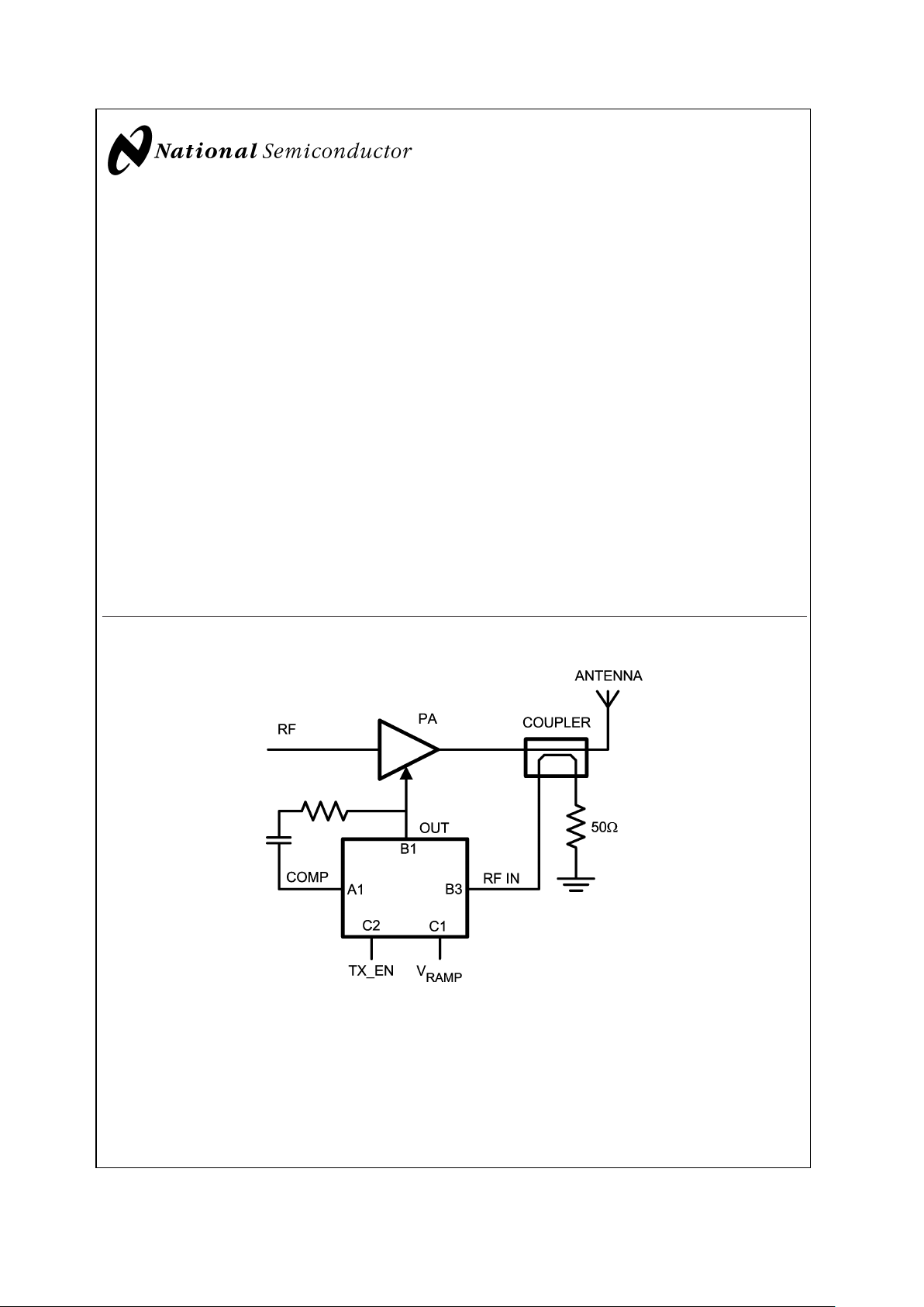
Typical Application
20029034
May 2002
LMV243 Single-Channel, Quad-Band GSM Power Controller in micro SMD
© 2002 National Semiconductor Corporation DS200290 www.national.com
Page 2

Absolute Maximum Ratings (Note 1)
If Military/Aerospace specified devices are required,
please contact theNational Semiconductor SalesOffice/
Distributors for availability and specifications.
Supply Voltage
V
DD
- GND 4V Max
ESD Tolerance (Note 2)
Human Body Model 2000V
Machine Model 200V
Storage Temperature Range −65˚C to 150˚C
Junction Temperature (Note 6) 150˚C Max
Mounting Temperature
Infrared or convection (20 sec) 235˚C
Operating Ratings (Note 1)
Nominal Supply Voltage 2.7V to 3.3V
Temperature Range −40˚C
<
T
J
<
85˚C
V
RAMP
Voltage Range 0V to 2V
V
HOME
Voltage Range 0V to 2V
RF Frequency Range 450MHz to 2GHz
Electrical Characteristics Unless otherwise specified, all limits are guaranteed to T
J
= 25˚C. VDD= 2.8V.
Boldface limits apply at temperature extremes.
Symbol Parameter Condition Min Typ Max Units
I
DD
Supply Current V
OUT
=(VDD- GND)/2 8.7 10.5
12.5
mA
In Shutdown (TX_EN = 0.8V)
V
OUT
=(VDD- GND)/2
4.6 30 µA
V
HIGH
Logic Level to Enable Power (Note 7) 1.8 V
V
LOW
Logic Level to Disable Power (Note 7) 0.8 V
T
ON
Turn-on- Time from Shutdown 3.7 6.5
7.5
µs
I
EN
Current into TX_EN Pin 0.108 5 µA
RAMP Amplifier
V
RD
V
RAMP
Deadband 170
150
210 250
270
mV
1/R
RAMP
Transconductance (Note 8) 78 µa/V
I
OUT RAMP
Ramp Amplifier Output Current V
RAMP
=2V 100 140 µA
RF Input
P
IN
RF Input Power Range (Note 5) 20kΩ // 27pF between V
OUT
and V
COMP
−50
+5
dBm
−63
−7
dBV
Logarithmic Slope (Note 9)
@
900MHz, 20kΩ // 27pF
between V
OUT
and V
COMP
−1.79
µa/dB
@
1800MHz, 20kΩ // 27pF
between V
OUT
and V
COMP
−1.89
@
1900MHz, 20kΩ // 27pF
between V
OUT
and V
COMP
−1.89
Logarithmic Intercept (Note 9)
@
900MHz, 20kΩ // 27pF
between V
OUT
and V
COMP
−50.5
dBm
@
1800MHz, 20kΩ // 27pF
between V
OUT
and V
COMP
−46.9
@
1900MHz, 20kΩ // 27pF
between V
OUT
and V
COMP
−45.9
R
IN
DC Resistance (Note 8) 50 Ω
C
IN
Input Capacitance (Note 8) 0.5 pF
Error Amplifier
GBW Gain-Bandwidth Product (Note 8) 7.6 MHz
LMV243
www.national.com 2
Page 3
Electrical Characteristics Unless otherwise specified, all limits are guaranteed to T
J
= 25˚C. VDD= 2.8V.
Boldface limits apply at temperature extremes. (Continued)
Symbol Parameter Condition Min Typ Max Units
V
O
Output Swing from Rail Sourcing, IO= 5mA 55 85
105
mV
Sinking, I
O
= −5mA 45 75
95
I
O
Output Short Circuit Current
(Note 3)
Sourcing, VO=0V 25 145
mA
Sinking, V
O
= 2.8V 25 180
e
n
Output Referred Noise RF input = 1800 MHz,
-10dBm, 20kΩ // 27pF
between V
OUT
and V
COMP
,
V
OUT
=1.4V, set by V
RAMP
,
(Note 8)
700 nV/
SR Slew Rate 8
5
11 V/µs
Note 1: Absolute Maximum Ratings indicate limits beyond which damage to the device may occur. Operating Ratings indicate conditions for which the device is
intended to be functional, but specific performance is not guaranteed. For guaranteed specifications and the test conditions, see the Electrical Characteristics.
Note 2: Human body model: 1.5kΩ in series with 100pF. Machine model, 0Ω in series with 100pF.
Note 3: Shorting circuit output to either V
+
or V−will adversely affect reliability.
Note 4: Electrical Table values apply only for factory testing conditions at the temperature indicated. Factory testing conditions result in very limited self-heating of
the device such that T
J=TA
. No guarantee of parametric performance is indicated in the electrical tables under conditions of internal self-heating where T
J
>
TA.
Note 5: Power in dBV = dBm + 13 when the impedance is 50Ω.
Note 6: The maximum power dissipation is a function of T
J(MAX)
, θJAand TA. The maximum allowable power dissipation at any ambient temperature is PD=
(T
J(MAX)-TA
)/θJA. All numbers apply for packages soldered directly into a PC board
Note 7: All limits are guaranteed by design or statistical analysis
Note 8: Typical values represent the most likely parametric norm.
Note 9: Slope and intercept are calculated from graphs ’V
OUT
vs. RF input Power’ where the current is obtained by division of the voltage by 20kΩ.
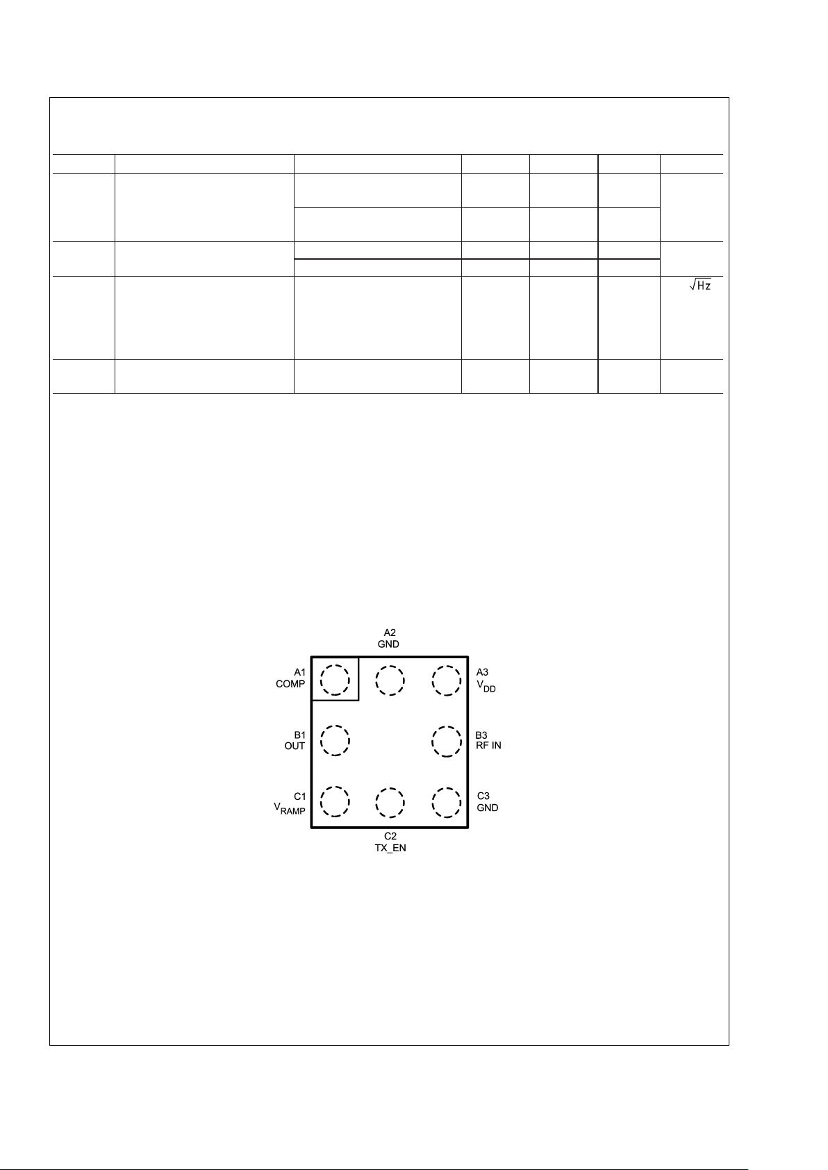
Connection Diagram
8-Bump micro SMD
20029035
Top View
LMV243
www.national.com3
Page 4
Pin Descriptions
Pin Name Description
Power Supply A3 V
DD
Supply Voltage
A2, C3 GND Power Ground. Operation requires both pins be grounded.
Digital Inputs C2 TX_EN A Logic High to enable device.
Analog Inputs B3 RF IN RF Input connected to the Coupler output with optional attenuation to measure the
Power Amplifier (PA) / Antenna RF power levels.
C1 RAMP IN Sets the RF output power level. The useful input voltage range is from 0.2V to 1.8V,
although voltages from 0V to V
DD
are allowed.
Compensation A1 Comp Connects an external RC network between the Comp pin and the Output pin for an
overall loop compensation and to control the closed loop frequency response.
Conventional loop stability techniques can be used in selecting this network, such as
Bode plots. A good starting value for the RC combination will be C = 68pF andR=0Ω.
Output B1 Out A rail-to-rail output capable of sourcing 25mA and sinking 25mA, with less than 200mV
total voltage drop over the specified temperature. The output is free from glitches when
enabled by TX_EN. When TX_EN is low, the output voltage is near GND.
Note: 1. All inputs and outputs are referenced to GND (pin A2, C3).
2. For the digital inputs, a LOW is
<
0.8V and a HIGH is>1.8V.
3. RF power detection is performed internally in the LMV243 and only an RF power coupler with optional extra attenuation has to be used.
Ordering Information
Package Part Number Package Marking Transport Media NSC Drawing
8-Bump micro SMD
LMV243BL 01 1k Units Tape and Reel
BLA08AAC
LMV243BLX 01 3k Units tape and Reel
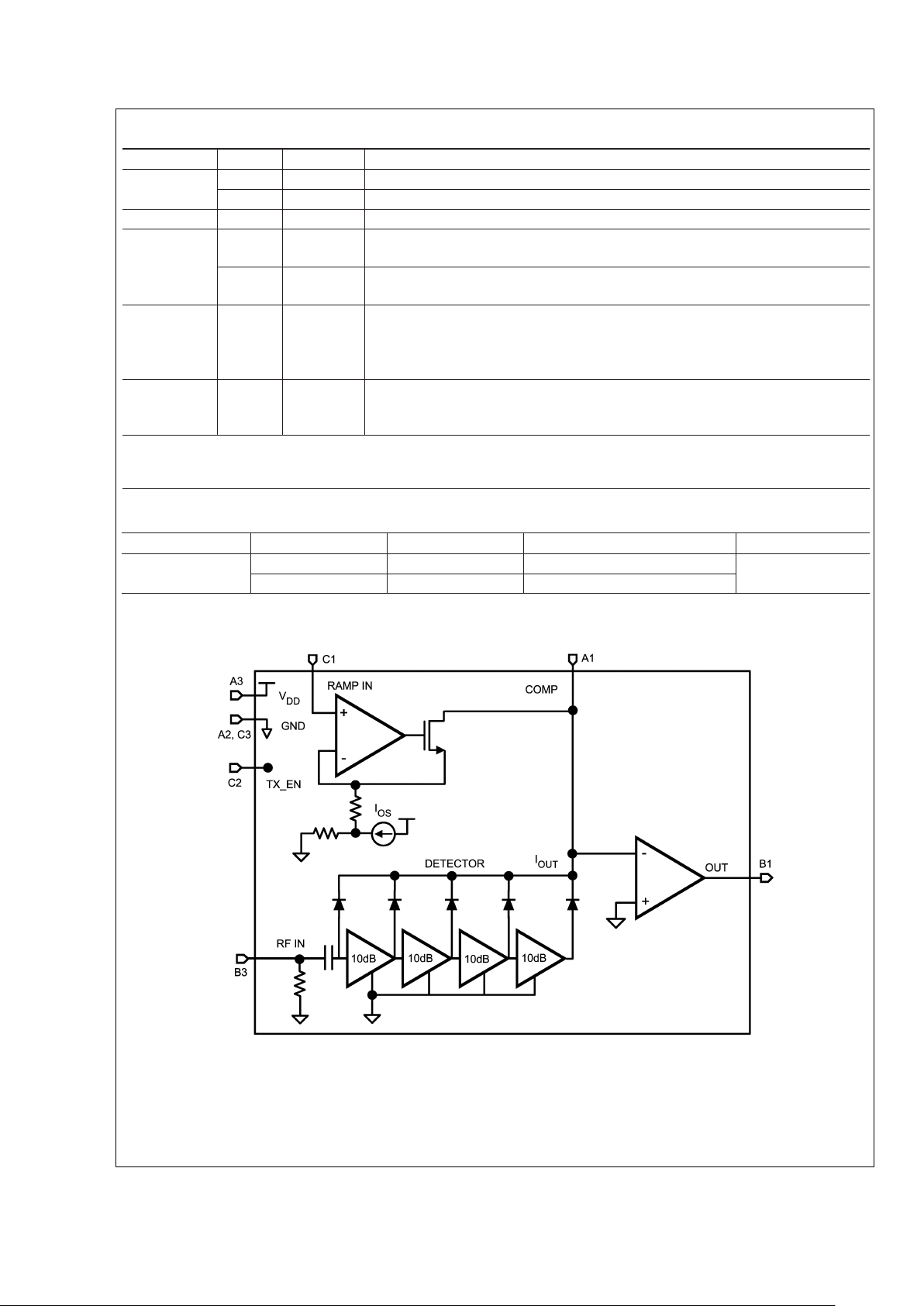
Block Diagram
20029036
FIGURE 1.
LMV243
www.national.com 4
Page 5

Typical Performance Characteristics Unless otherwise specified, V
DD
= +2.8V, TJ= 25˚C.
Supply Current vs. Supply Voltage V
OUT
and Log Conformance vs. RF Input Power
20029024
20029001
V
OUT
and Log Conformance vs. RF Input Power at
Corners of GSM
V
OUT
and Log Conformance vs. RF Input Power at
Corners of DCS
20029002 20029008
V
OUT
and Log Conformance vs. Pin@Corners of PCS
V
OUT
and Log Conformance vs. RF Input Power at
900MHz
20029009
20029003
LMV243
www.national.com5
Page 6

Typical Performance Characteristics Unless otherwise specified, V
DD
= +2.8V, TJ=
25˚C. (Continued)
V
OUT
and Log Conformance vs. RF Input Power at
1800MHz
V
OUT
and Log Conformance vs. RF Input Power at
1900MHz
20029004 20029005
Logarithmic Slope vs. Frequency Logarithmic Intercept vs. Frequency
20029006 20029007
RF Input Impedance vs. Frequency@Resistance and
Reactance Gain and Phase vs. Frequency Error Amplifier
20029031
20029026
LMV243
www.national.com 6
Page 7

Typical Performance Characteristics Unless otherwise specified, V
DD
= +2.8V, TJ=
25˚C. (Continued)
I
COMP
vs. V
RAMP
PINvs. V
RAMP
20029027
20029028
Sourcing Current vs. Output Voltage Sinking Current vs. Output Voltage
20029032
20029033
Output Voltage vs. Sourcing Current Output Voltage vs. Sinking Current
20029029
20029030
LMV243
www.national.com7
Page 8

Typical Performance Characteristics Unless otherwise specified, V
DD
= +2.8V, TJ=
25˚C. (Continued)
Closed Loop P
OUT
(PA) vs. V
RAMP
@
900MHz Closed Loop P
OUT
(PA) vs. V
RAMP
@
1800MHz
20029011 20029012
Closed Loop P
OUT
(PA) vs. V
RAMP
@
1900MHz Time Mask Plot vs. Time@900MHz
20029013
20029014
Time Mask Plot vs. Time@1800MHz Time Mask Plot vs. Time@1900MHz
20029015 20029016
LMV243
www.national.com 8
Page 9

Application Information
1.0 The LMV243 as an RF Power Amplifier (PA) Controller
The LMV243 is a member of the power loop controller family
of National Semiconductor, for a quad-band TDMA/GSM
solution. The typical application diagram demonstrates a
basic approach for implementing the quad-band solution
around the RF Power Amplifier. The LMV243 contains a 50
dB Logamp detector and interfaces directly with the directional coupler.
The LMV243 Base Band (control) interface consists of 2
signals:
TX_EN
to bring the device out of shutdown status
within 5µs, and V
RAMP
for the transmit burst characteristic
determining the desired Output Power level. The LMV243
gives maximum flexibility to meet GSM frequency and time
mask criteria for many different single supply Power Amplifier types like HBT or, MesFET in GaAs, SiGe or Si technology.This is accomplished by the Programmable Ramp characteristic from the Base Band and the TX_EN signal along
with the external compensation capacitor.
Power consumption requirements are supported by the
TX_EN function which puts the entire chip into a Power
Saving Mode to enable maximum standby and talk time
while ensuring the output does not glitch excessively during
Power-up and Power-down.
2.0 A Typical GSM Power Amplifier Controlled Loop
This section should give a general overviewand understanding of how a typical Power Amplifier control loop works and
how to get rid of some of the most common problems
confronted in the design.
Figure 2
shows the generic components of such a loop. Beginning at the output of the GSM
Power Amplifier (PA), this signal is fed, usually via a directional coupler, to a detector.The output current of the detector Idet drives the inverting input of an op amp, configuredas
an integrator. A reference voltage drives the non-inverting
input of the op amp. Finally the output of the op amp integrator drives the gain control input of the power amplifier.
Now to examine how this circuit works, we will assume
initially that the output of the PA is atsome low level and that
the V
RAMP
voltage is at 1V. The V/I converter converts the
V
RAMP
voltage to a sinking current I
RAMP
. This current can
only come from the integrator capacitor C. Current flow in
this direction increases the output voltage of the integrator.
This voltage, which drives the PA, increases the gain (we
assume that the PA’s gain control input has a positive sense,
that is, increasing voltage increases gain). The gain will
increase, thereby increasing the amplifier’s output level until
the detector output current equals the ramp currentI
RAMP
.At
that point, the current through the capacitor will decrease to
zero and the integrator output will be held steady, thereby
settling the loop. If capacitor charge is lost over time, the
gain will decrease. However, this leakage will quickly be
corrected by additional integrator current from the newly
reduced detector current.
The key usefulness of this circuit lies in its immunity to
changes in the PA gain control function. From a static perspective at least, the relationship between gain and gain
control voltage is of no consequence to the overall transfer
function. Based upon the value of V
RAMP
, the integrator will
set the gain control voltage to whatever level is necessary to
produce the desired output level. Any temperature dependency in the gain control function will be eliminated. Also,
non-linearity’s in the gain transfer function of the PA do not
appear in the overall transfer function (V
OUT
vs. V
RAMP
). The
only requirement isthat the gaincontrol function ofthe PAbe
monotonic. It is crucial, however, that the detector is temperature stable.
The circuit as described so far, has been designed to produce a constant output level for varying input levels. The
only requirement is for it to be temperature stable for input
levels that correspond to the setpoint voltage V
RAMP
.Ifthe
detector used has a higher dynamic range, the circuit to
precisely set PA output levels over a wide dynamic range. To
do this, the integrator reference voltage, V
RAMP
, is varied.
The voltage range on V
RAMP
follows directly from the detec-
tor’s transfer function. For example, if the detector delivers
0.5V for an input of −7dBm, a reference voltage of 0.5V will
cause the loop to settle when the detector input is −7dBm
(the PA output will be greater than this amount by whatever
coupling factor exists between PA and detector). The dynamic range for the variable RF P
OUT
case will be determined by the device in the circuit with the least dynamic
range (i.e. the gain control range PA or linear dynamic of
detector).
20029037
FIGURE 2. PA Control Loop
LMV243
www.national.com9
Page 10

Application Information (Continued)
The response time of this loop can be controlled by varying
the RC time constant of the integrator. Setting this at a low
level will result in fast output settling but can result in ringing
in the output envelope. Settling the RC time constant high
will give the loop good stability but will increase settling time.
Figure 3
shows a typical RF power control loop realized by
using the National’s LMV243 with integrated RF detector.
The RF signal from the PA passes through a directional
coupler on its way to the antenna. Directional couplers are
characterized by their coupling factor which is in the 10dB to
30dB range, typical 20dB. Because the coupled output must
in its own right deliver some power (in this case to the
detector), the coupling process takes some power from the
main output. This manifests itself as insertion loss, the insertion loss being higher for lower coupling factors.
3.0 Attenuation between coupler and LMV243 detector
It is very important to choose the right attenuation between
PAoutput and detector input, i.e. the total of coupling factor
and extra attenuation, in order to achieve power control over
the full output power range of the PA. A typical value for the
output power of the PA is +35.5 dBm for GSM and +30 dBm
for PCS/DCS. In order to accommodate these levels into the
LMV243 detection range the minimum required total attenuation is about 35 dBm (please refer to typical performance
characteristics in the datasheet). A typical coupler factor is
20dB. An extra attenuation of about 15 dB should be inserted.
Extra attenuation Z between the coupler and the RF input of
the LMV243 can be achieved by 2 resistors R
X
and R
Y
according to
Figure 3
, where
Z = 20 log [R
IN
/(RIN+RY)]
e.g. R
Y
= 300Ω results in an attenuation of 16.9dB.
To prevent reflection back to the coupler the impedance
seen by the coupler should be 50Ω. The impedance R
O
consists of RX// (RY,RO,+RIN). RXcan be calculated with
the formula:
R
X
=[RO*(RY+RIN)]/R
Y
RX=50*[1 + (50/RY)]
e.g. with R
Y
= 300Ω,RIN=50Ω→RX=58Ω.
4.0 Components of a Power Amplifier Loop
Figure 3
shows the basics of a typical LMV243 quad-band
application.
The key components are:
•
The LMV243
•
One power amplifier, usually for the GSM and PCN/DCS
bands
•
A single two channel RF coupler is used instead of the
two RF couplers
•
A dual or quad-band antenna.
Figure 1
shows the LMV243’s internal architecture. The
LMV243 contains an RF detector, error amplifier, a ramp V/I
converter and an output driver. The LMV243 input interface
consists of an RF input, Ramp voltage, and a digital input to
perform the function ’Shutdown/Transmit Enable’.
5.0 Analog and Digital Input Signals of the LMV243
The LMV243 has the following inputs:
–V
RAMP
is an analog signal (Base band DAC ramp signal)
–TX_EN is a digital signal (performs the function ‘Shutdown/
Transmit Enable’).
5.1 V
RAMP
in signal
The actual V
RAMP
input value sets the RF output power. By
applying a certain mask shape to the ’Ramp in’ pin, the
output voltage level of the LMV243 adjusts the PA control
voltage to get a power level (P
OUT
/dBm) out of the PA which
is proportional to the single ramp voltage steps. The recommended V
RAMP
voltage range forRF power control is 0.2V to
2.0V. The V
RAMP
input will tolerate voltages from 0V to V
DD
without malfunction or damage. The V
RAMP
input does not
change the output level until the level reaches about 200mV,
so offset voltages in the DAC or amplifier supplying the
Ramp signal will not cause excess RF signal output and
increased power consumption.
6.0 Analog Output
The Output is driven by a rail-to-railamplifier capable of both
sourcing and sinking. It is able to source and sink 25mA with
less than 200mV voltage drop from either rail over recommended operating conditions. Please refer to the typical
performance characteristics. The output voltage vs.
Sourcing/Sinking current show the typical voltage drop from
the rail over temperature. The Sourcing/Sinking current vs.
output voltage characteristics show the typical
charging/discharging current, which the output is capable of
delivering at a current voltage. The output is free from
glitches when enabled by TX_EN. When TX_EN is low, the
selected output voltage is fixed or near GND.
7.0 Bandwidth Compensation
To compensate and prevent the closed loop arrangement
from oscillations and overshoots at the output of the RF
detector/error amplifier LMV243, the system can be adjusted
by means of external RC components connected between
Comp and Out . Exact values heavily depend on PA characteristics. A good starting point isR=0Ωand C = 68pF. The
vast combinations of PA’s and couplers available preclude a
generalized formula for choosing these component. Please
contact National Semiconductor for additional assistance.
8.0 Evaluation Board
An evaluation board in available for the LMV243. Please
contact your local distributor or National Semiconductor
sales office.
20029038
FIGURE 3. PA Control Loop With Extra Attenuation
LMV243
www.national.com 10
Page 11

Typical Timing Diagram
20029039
LMV243
www.national.com11
Page 12

Typical Test Setup Diagram
20029022
Equipment List:
RF Signal Generator Rohde & Schwarz SMIQ 03B
Pulse Generator Tektronix AFG2020
Spectrum Analyzer Rohde & Schwarz FSP
Power Meter HP E4418B, with Powersensor HP E4413A
Coupler Pasternack PE 2208-10
LMV243
www.national.com 12
Page 13

Physical Dimensions inches (millimeters)
unless otherwise noted
8-Bump micro SMD
NS Package Number BLA08AAC
X1 = 1.514
±
0.03mm X2 = 1.514±0.03mm X3 = 0.995±0.1mm
NOTES: UNLESS OTHERWISE SPECIFIED
1. EPOXY COATING
2.Sn/37Pb EUTECTIC BUMP
3. RECOMMEND NON-SOLDER MASK DEFINED LANDING PAD.
4. PIN A1 IS ESTABLISHED BY LOWER LEFT CORNER WITH RESPECT TO TEXT ORIENTATION. REMAINING PINS ARE NUMBERED COUNTER
CLOCKWISE.
5.XXX IN DRAWING NUMBER REPRESENTS PACKAGE SIZE VARIATION WHERE X1 IS PACKAGE WIDTH, X2 IS PACKAGE LENGTH AND X3 IS
PACKAGE HEIGHT.
REFERENCE JEDEC REGISTRATION MO-211, VARIATION BC.
LIFE SUPPORT POLICY
NATIONAL’S PRODUCTS ARE NOT AUTHORIZED FOR USE AS CRITICAL COMPONENTS IN LIFE SUPPORT
DEVICES OR SYSTEMS WITHOUT THE EXPRESS WRITTEN APPROVAL OF THE PRESIDENT AND GENERAL
COUNSEL OF NATIONAL SEMICONDUCTOR CORPORATION. As used herein:
1. Life support devices or systems are devices or
systems which, (a) are intended for surgical implant
into the body, or (b) support or sustain life, and
whose failure to perform when properly used in
accordance with instructions for use provided in the
labeling, can be reasonably expected to result in a
significant injury to the user.
2. A critical component is any component of a life
support device or system whose failure to perform
can be reasonably expected to cause the failure of
the life support device or system, or to affect its
safety or effectiveness.
National Semiconductor
Corporation
Americas
Email: support@nsc.com
National Semiconductor
Europe
Fax: +49 (0) 180-530 85 86
Email: europe.support@nsc.com
Deutsch Tel: +49 (0) 69 9508 6208
English Tel: +44 (0) 870 24 0 2171
Français Tel: +33 (0) 1 41 91 8790
National Semiconductor
Asia Pacific Customer
Response Group
Tel: 65-2544466
Fax: 65-2504466
Email: ap.support@nsc.com
National Semiconductor
Japan Ltd.
Tel: 81-3-5639-7560
Fax: 81-3-5639-7507
www.national.com
LMV243 Single-Channel, Quad-Band GSM Power Controller in micro SMD
National does not assume any responsibility for use of any circuitry described, no circuit patent licenses are implied and National reserves the right at any time without notice to change said circuitry and specifications.
 Loading...