

Page 1
December 2006
LMV221
50 MHz to 3.5 GHz 40 dB Logarithmic Power Detector for
CDMA and WCDMA
General Description
The LMV221 is a 40 dB RF power detector intended for use
in CDMA and WCDMA applications. The device has an RF
frequency range from 50 MHz to 3.5 GHz. It provides an accurate temperature and supply compensated output voltage
that relates linearly to the RF input power in dBm. The circuit
operates with a single supply from 2.7V to 3.3V.
The LMV221 has an RF power detection range from −45 dBm
to −5 dBm and is ideally suited for direct use in combination
with a 30 dB directional coupler. Additional low-pass filtering
of the output signal can be realized by means of an external
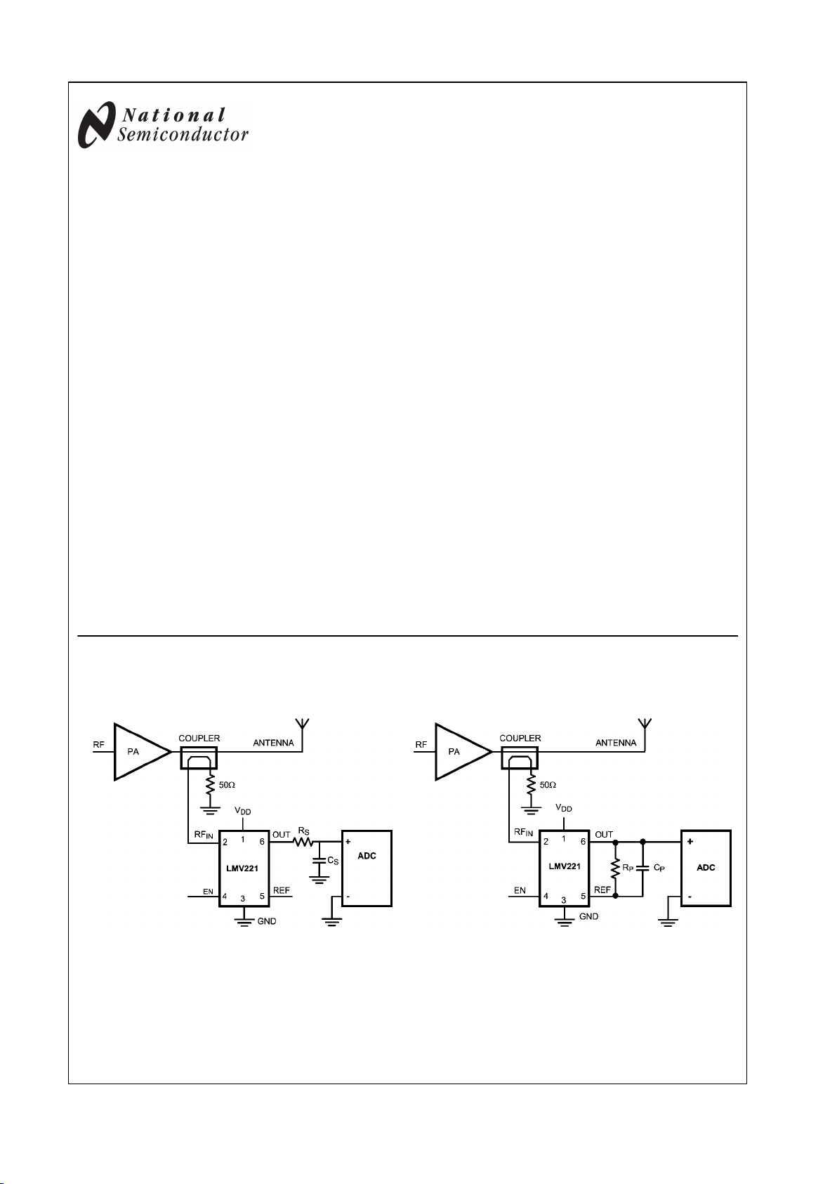
resistor and capacitor. Figure (a) shows a detector with an
additional output low pass filter. The filter frequency is set with
RS and CS.
Figure (b) shows a detector with an additional feedback low
pass filter. Resistor RP is optional and will lower the Trans
impedance gain (R
TRANS
). The filter frequency is set with
CP//C
TRANS
and RP//R
TRANS
.
The device is active for Enable = High, otherwise it is in a low
power consumption shutdown mode. To save power and prevent discharge of an external filter capacitance, the output
(OUT) is high-impedance during shutdown.
The LMV221 power detector is offered in the small 2.2 mm x
2.5 mm x 0.8 mm LLP package.
Features
■
40 dB linear in dB power detection range
■
Output voltage range 0.3 to 2V
■
Shutdown
■
Multi-band operation from 50 MHz to 3.5 GHz
■
0.5 dB accurate temperature compensation
■
External configurable output filter bandwidth
■
2.2 mm x 2.5 mm x 0.8 mm LLP 6 package
Applications
■
UMTS/CDMA/WCDMA RF power control
■
GSM/GPRS RF power control
■
PA modules
■
IEEE 802.11b, g (WLAN)
Typical Application
(a) LMV221 with output RC Low Pass Filter
20173771
(b) LMV221 with feedback (R)C Low Pass Filter
20173704
© 2007 National Semiconductor Corporation 201737 www.national.com
LMV221 50 MHz to 3.5 GHz 40 dB Logarithmic Power Detector for CDMA and WCDMA
Page 2

Absolute Maximum Ratings (Note 1)
If Military/Aerospace specified devices are required,
please contact the National Semiconductor Sales Office/
Distributors for availability and specifications.
Supply Voltage
VDD - GND
3.6V
RF Input
Input power 10 dBm
DC Voltage 400 mV
Enable Input Voltage VSS - 0.4V < V
EN
< VDD + 0.4V
ESD Tolerance (Note 2)
Human Body Model 2000V
Machine Model 200V
Charge Device Model 2000V
Storage Temperature
Range −65°C to 150°C
Junction Temperature
(Note 3) 150°C
Maximum Lead Temperature
(Soldering,10 sec) 260°C
Operating Ratings (Note 1)
Supply Voltage 2.7V to 3.3V
Temperature Range −40°C to +85°C
RF Frequency Range 50 MHz to 3.5 GHz
RF Input Power Range (Note 5) −45 dBm to −5 dBm
−58 dBV to −18 dBV
Package Thermal Resistance θ
JA
(Note 3) 86.6°C/W
2.7 V DC and AC Electrical Characteristics
Unless otherwise specified, all limits are guaranteed to; TA = 25°C, VDD = 2.7V, RF input frequency f = 1855 MHz CW (Continuous
Wave, unmodulated). Boldface limits apply at the temperature extremes (Note 4).
Symbol Parameter Condition Min
(Note 6)
Typ
(Note 7)
Max
(Note 6)
Units
Supply Interface
I
DD
Supply Current Active mode: EN = High, no Signal
present at RFIN.
6.5
5
7.2 8.5
10
mA
Shutdown: EN = Low, no Signal present
at RFIN.
0.5 3
4
μA
EN = Low: PIN = 0 dBm (Note 8) 10
Logic Enable Interface
V
LOW
EN Logic Low Input Level
(Shutdown mode)
0.6 V
V
HIGH
EN Logic High Input Level 1.1 V
I
EN
Current into EN Pin 1
μA
RF Input Interface
R
IN
Input Resistance 40 47.1 60
Ω
Output Interface
V
OUT
Output Voltage Swing From Positive Rail, Sourcing,
V
REF
= 0V, I
OUT
= 1 mA
16 40
50
mV
From Negative Rail, Sinking,
V
REF
= 2.7V, I
OUT
= 1 mA
14 40
50
I
OUT
Output Short Circuit Current Sourcing, V
REF
= 0V, V
OUT
= 2.6V 3
2.7
5.4
mA
Sinking, V
REF
= 2.7V, V
OUT
= 0.1V 3
2.7
5.7
BW Small Signal Bandwidth No RF input signal. Measured from REF
input current to V
OUT
450 kHz
R
TRANS
Output Amp Transimpedance
Gain
No RF Input Signal, from I
REF
to V
OUT
,
DC
35 42.7 55
kΩ
SR Slew Rate Positive, V
REF
from 2.7V to 0V 3
2.7
4.1
V/µs
Negative, V
REF
from 0V to 2.7V 3
2.7
4.2
R
OUT
Output Impedance
(Note 8)
No RF Input Signal, EN = High. DC
measurement
0.6 5
6
Ω
www.national.com 2
LMV221
Page 3

Symbol Parameter Condition Min
(Note 6)
Typ
(Note 7)
Max
(Note 6)
Units
I
OUT,SD
Output Leakage Current in
Shutdown mode
EN = Low, V
OUT
= 2.0V 21 300
500
nA
RF Detector Transfer
V
OUT,MAX
Maximum Output Voltage
PIN= −5 dBm
(Note 8)
f = 50 MHz 1.67 1.76 1.83
V
f = 900 MHz 1.67 1.75 1.82
f = 1855 MHz 1.53 1.61 1.68
f = 2500 MHz 1.42 1.49 1.57
f = 3000 MHz 1.33 1.40 1.48
f = 3500 MHz 1.21 1.28 1.36
V
OUT,MIN
Minimum Output Voltage
(Pedestal)
No input Signal 175
142
250 350
388
mV
ΔV
OUT,MIN
Pedestal Variation over
temperature
No Input Signal, Relative to 25°C −20 20 mV
ΔV
OUT
Output Voltage Range
PIN from −45 dBm to −5 dBm
(Note 8)
f = 50 MHz 1.37 1.44 1.52
V
f = 900 MHz 1.34 1.40 1.47
f = 1855 MHz 1.24 1.30 1.37
f = 2500 MHz 1.14 1.20 1.30
f = 3000 MHz 1.07 1.12 1.20
f = 3500 MHz 0.96 1.01 1.09
K
SLOPE
Logarithmic Slope
(Note 8)
f = 50 MHz 39 40.5 42
mV/dB
f = 900 MHz 36.7 38.5 40
f = 1855 MHz 34.4 35.7 37.1
f = 2500 MHz 32.6 33.8 35.2
f = 3000 MHz 31 32.5 34
f = 3500 MHz 30 31.9 33.5
P
INT
Logarithmic Intercept
(Note 8)
f = 50 MHz −50.4 −49.4 −48.3
dBm
f = 900 MHz −54.1 −52.8 −51.6
f = 1855 MHz −53.2 −51.7 −50.2
f = 2500 MHz −51.8 −50 −48.3
f = 3000 MHz −51.1 −48.9 −46.6
f = 3500 MHz −49.6 −46.8 −44.1
t
ON
Turn-on Time
(Note 8)
No signal at PIN, Low-High transition
EN. V
OUT
to 90%
8 10
12
µs
t
R
Rise Time (Note 9) PIN = No signal to 0 dBm, V
OUT
from 10%
to 90%
2 12 µs
t
F
Fall Time (Note 9) PIN = 0 dBm to no signal, V
OUT
from 90%
to 10%
2 12 µs
e
n
Output Referred Noise
(Note 9)
PIN = −10 dBm, at 10 kHz 1.5
µV/
v
N
Output referred Noise
(Note 8)
Integrated over frequency band
1 kHz - 6.5 kHz
100 150
µV
RMS
PSRR Power Supply Rejection Ratio
(Note 9)
PIN = −10 dBm, f = 1800 MHz 55 60 dB
3 www.national.com
LMV221
Page 4

Symbol Parameter Condition Min
(Note 6)
Typ
(Note 7)
Max
(Note 6)
Units
Power Measurement Performance
E
LC
Log Conformance Error
(Note 8)
−40 dBm ≤ PIN ≤ −10 dBm
f = 50 MHz −0.60
−1.10
0.53 0.56
1.3
dB
f = 900 MHz −0.70
−1.24
0.46 0.37
1.1
f = 1855 MHz −0.40
−1.1
0.48 0.24
1.1
f = 2500 MHz −0.43
−1.0
0.51 0.56
1.1
f = 3000 MHz −0.87
−1.2
0.56 1.34
1.6
f = 3500 MHz −1.73
−2.0
0.84 2.72
2.7
E
VOT
Variation over Temperature
(Note 8)
−40 dBm ≤ PIN ≤ −10 dBm
f = 50 MHz −1.1 0.4 1.4
dB
f = 900 MHz −1.0 0.38 1.27
f = 1855 MHz −1.1 0.44 1.31
f = 2500 MHz −1.1 0.48 1.15
f = 3000 MHz −1.2 0.5 0.98
f = 3500 MHz –1.2 0.62 0.85
E
1 dB
Measurement Error for a 1 dB
input power step (Note 8)
−40 dBm ≤ PIN ≤ −10 dBm
f = 50 MHz −0.06 0.069
dB
f = 900 MHz −0.056 0.056
f = 1855 MHz −0.069 0.069
f = 2500 MHz −0.084 0.084
f = 3000 MHz −0.092 0.092
f = 3500 MHz −0.10 0.10
E
10 dB
Measurement Error for a 10 dB
input power step (Note 8)
−40 dBm ≤ PIN ≤ −10 dBm
f = 50 MHz −0.65 0.57
dB
f = 900 MHz −0.75 0.58
f = 1855 MHz −0.88 0.72
f = 2500 MHz −0.86 0.75
f = 3000 MHz −0.85 0.77
f = 3500 MHz −0.76 0.74
S
T
Temperature Sensitivity
−40°C < TA < 25°C (Note 8)
−40 dBm ≤ PIN ≤ −10 dBm
f = 50 MHz −15 −7 1
mdB/°C
f = 900 MHz −13.4 −6 1.5
f = 1855 MHz −14.1 −5.9 2.3
f = 2500 MHz −13.4 −4.1 5.2
f = 3000 MHz −11.7 −1.8 8
f = 3500 MHz −10.5 0.5 1.2
S
T
Temperature Sensitivity
25°C < TA < 85°C (Note 8)
−40 dBm ≤ PIN ≤ −10 dBm
f = 50 MHz −12.3 −6.7 −1.1
mdB/°C
f = 900 MHz −13.1 −6.7 −0.2
f = 1855 MHz −14.7 −7.1 0.42
f = 2500 MHz −15.9 −7.6 0.63
f = 3000 MHz −18 −8.5 1
f = 3500 MHz −21.2 −9.5 2.5
S
T
Temperature Sensitivity
−40°C < TA < 25°C, (Note 8)
PIN = −10 dBm
f = 50 MHz −15.8 −8.3 −0.75
mdB/°C
f = 900 MHz −14.2 −6 2.2
f = 1855 MHz −14.9 −7.4 2
f = 2500 MHz −14.5 −6.6 1.3
f = 3000 MHz −13 −4.9 3.3
f = 3500 MHz −12 −3.4 5.3
www.national.com 4
LMV221
Page 5

Symbol Parameter Condition Min
(Note 6)
Typ
(Note 7)
Max
(Note 6)
Units
S
T
Temperature Sensitivity
25°C < TA < 85°C, (Note 8)
PIN = −10 dBm
f = 50 MHz −12.4 −8.9 −5.3
mdB/°C
f = 900 MHz −13.7 −9.4 −5
f = 1855 MHz −14.6 −10 −5.6
f = 2500 MHz −15.2 −10.8 −6.5
f = 3000 MHz −16.5 −12.2 −7.9
f = 3500 MHz −18.1 −13.5 −9
P
MAX
Maximum Input Power for
ELC = 1 dB(Note 8)
f = 50 MHz −8.85 −5.9
dBm
f = 900 MHz −9.3 −6.1
f = 1855 MHz −8.3 −5.5
f = 2500 MHz −6 −4.2
f = 3000 MHz −5.4 −3.7
f = 3500 MHz −7.2 −2.7
P
MIN
Minimum Input Power for
ELC = 1 dB (Note 8)
f = 50 MHz −40.3 −38.9
dBm
f = 900 MHz −44.2 −42.9
f = 1855 MHz −42.9 −41.2
f = 2500 MHz −40.4 −38.6
f = 3000 MHz −38.4 −35.8
f = 3500 MHz −35.3 −31.9
DR Dynamic Range for ELC = 1 dB
(Note 8)
f = 50 MHz 31.5 34.5
dB
f = 900 MHz 34.4 38.1
f = 1855 MHz 34 37.4
f = 2500 MHz 33.8 36.1
f = 3000 MHz 32.4 34.8
f = 3500 MHz 26.2 32.7
Note 1: Absolute Maximum Ratings indicate limits beyond which damage to the device may occur. Operating Ratings indicate conditions for which the device is
intended to be functional, but specific performance is not guaranteed. For guaranteed specifications and the test conditions, see the Electrical Characteristics.
Note 2: Human body model, applicable std. MIL-STD-883, Method 3015.7. Machine model, applicable std. JESD22–A115–A (ESD MM std of JEDEC). FieldInduced Charge-Device Model, applicable std. JESD22–C101–C. (ESD FICDM std. of JEDEC)
Note 3: The maximum power dissipation is a function of T
J(MAX)
, θJA. The maximum allowable power dissipation at any ambient temperature is
PD = (T
J(MAX)
- TA)/θJA. All numbers apply for packages soldered directly into a PC board.
Note 4: Electrical Table values apply only for factory testing conditions at the temperature indicated. Factory testing conditions result in very limited self-heating
of the device such that TJ = TA. No guarantee of parametric performance is indicated in the electrical tables under conditions of internal self-heating where
TJ > TA.
Note 5: Power in dBV = dBm + 13 when the impedance is 50Ω.
Note 6: All limits are guaranteed by design or statistical analysis.
Note 7: Typical values represent the most likely parametric norm as determined at the time of characterization. Actual typical values may vary over time and will
also depend on the application and configuration. The typical values are not tested and are not guaranteed on shipped production material.
Note 8: All limits are guaranteed by design and measurements which are performed on a limited number of samples. Limits represent the mean ±3–sigma values.
The typical value represents the statistical mean value.
Note 9: This parameter is guaranteed by design and/or characterization and is not tested in production.
5 www.national.com
LMV221
Page 6
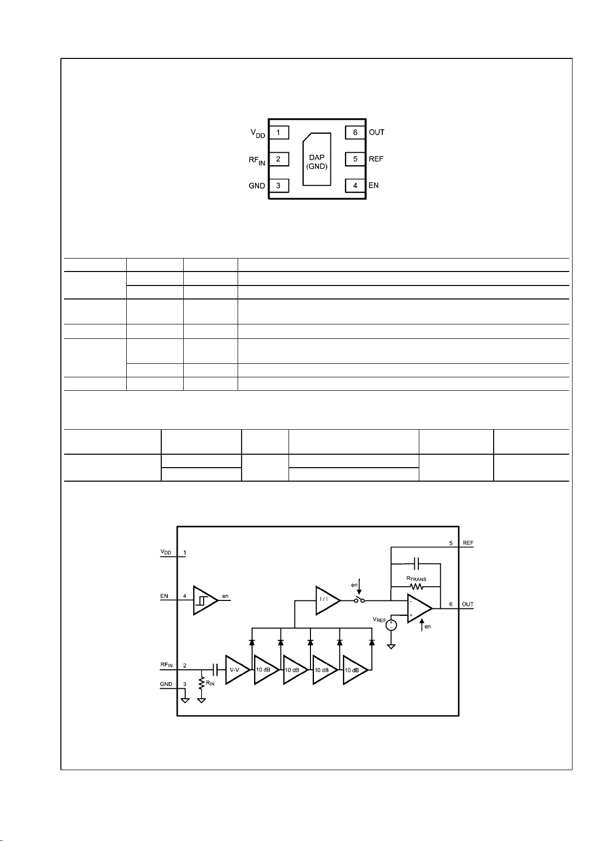
Connection Diagram
6-pin LLP
20173702
Top View
Pin Descriptions
LLP6 Name Description
Power Supply 1 V
DD
Positive Supply Voltage
3 GND Power Ground
Logic Input 4 EN The device is enabled for EN = High, and brought to a low-power shutdown mode for
EN = Low.
Analog Input 2 RF
IN
RF input signal to the detector, internally terminated with 50 Ω.
Output 5 REF Reference output, for differential output measurement (without pedestal). Connected to
inverting input of output amplifier.
6 OUT Ground referenced detector output voltage (linear in dB)
DAP GND Ground (needs to be connected)
Ordering Information
Package Part Number Package
Marking
Transport Media NSC Drawing Status
LLP-6
LMV221SD
A96
1k Units Tape and Reel
SDB06A Released
LMV221SDX 4.5k Units Tape and Reel
Block Diagram
20173703
LMV221
www.national.com 6
LMV221
Page 7
Typical Performance Characteristics Unless otherwise specified, V
DD
= 2.7V,
TA = 25°C, measured on a limited number of samples.
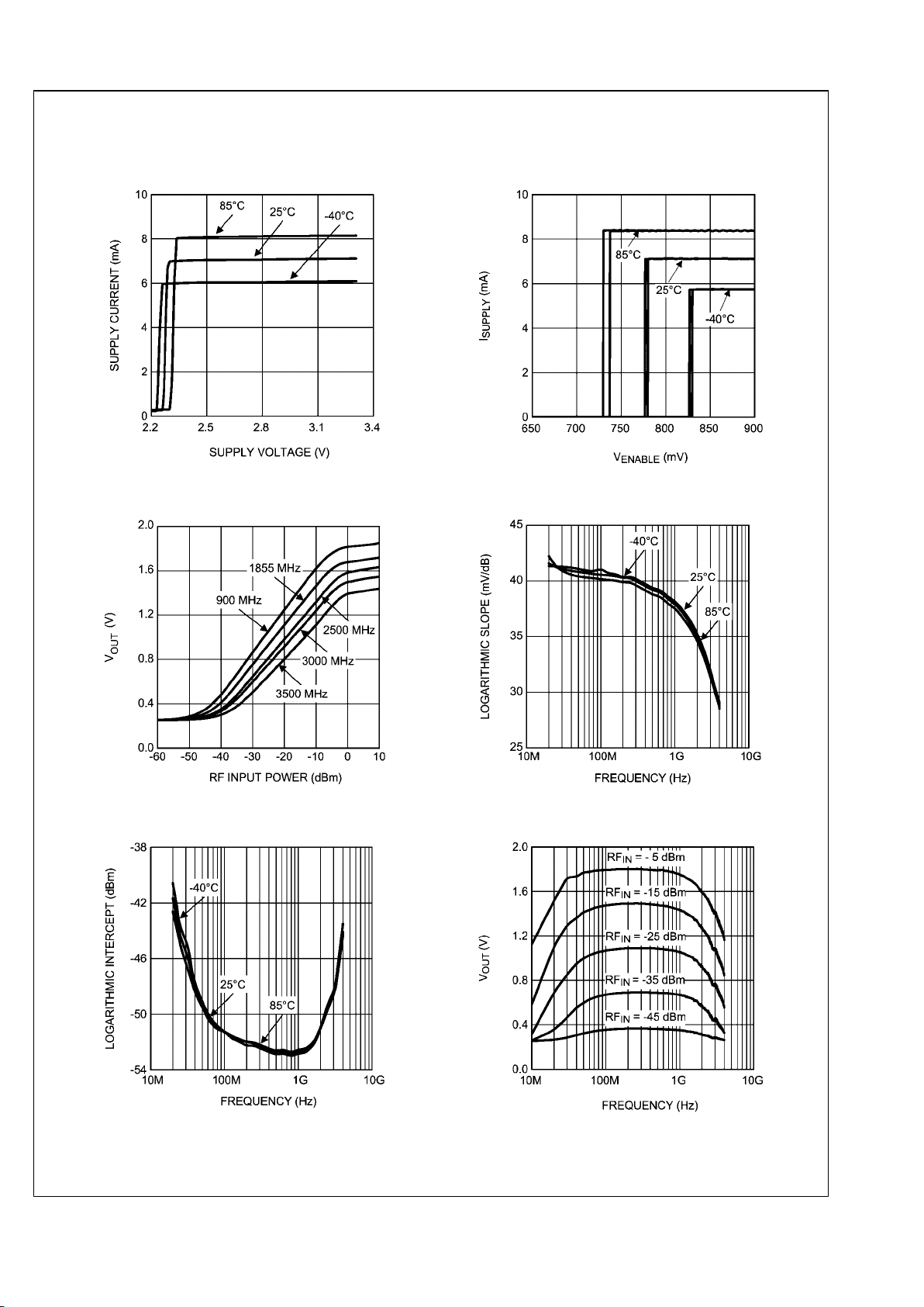
Supply Current vs. Supply Voltage
20173705
Supply Current vs. Enable Voltage
20173708
Output Voltage vs. RF input Power
20173712
Log Slope vs. Frequency
20173746
Log Intercept vs. Frequency
20173749
Output Voltage vs. Frequency
20173713
7 www.national.com
LMV221
Page 8
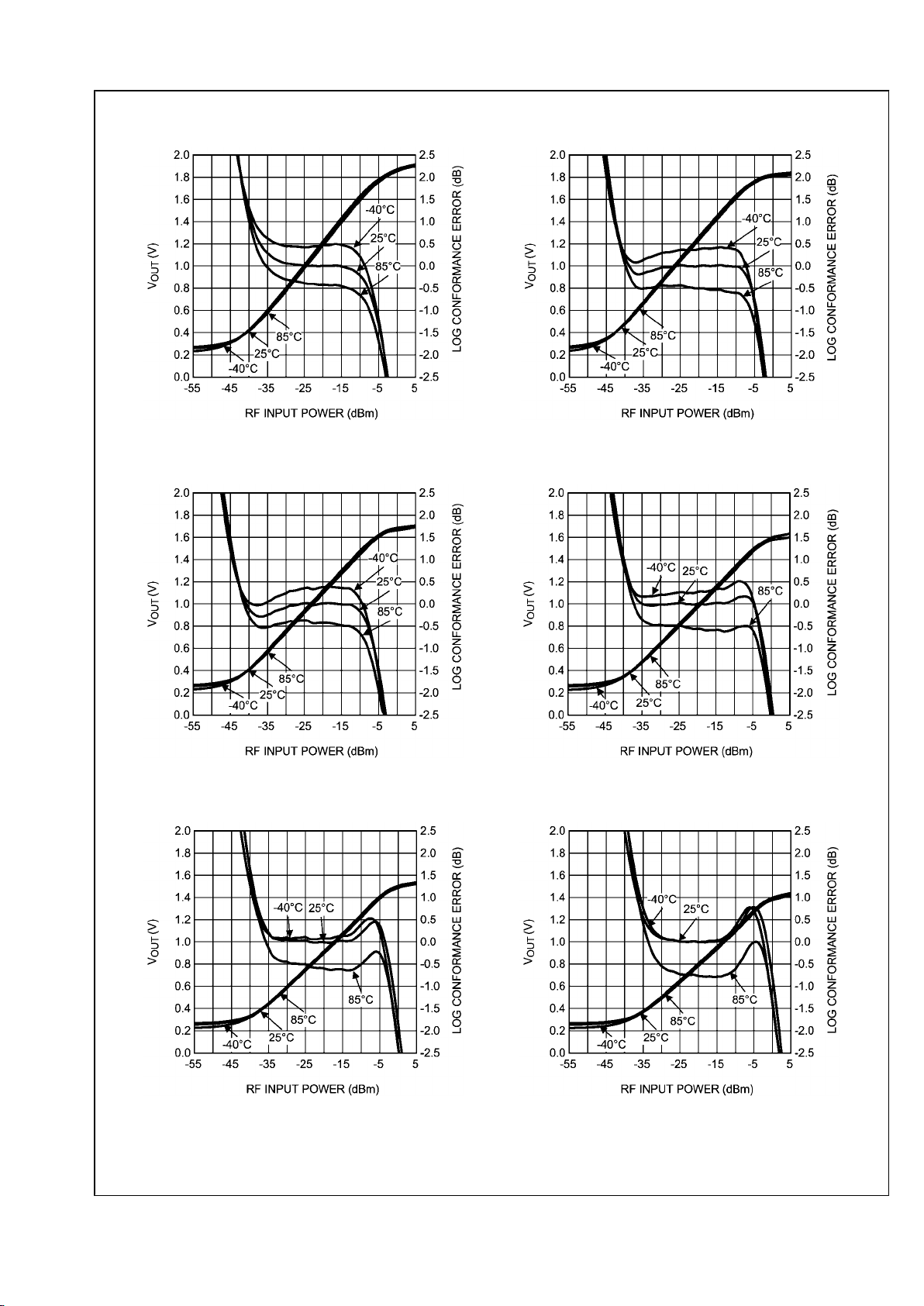
Mean Output Voltage and Log Conformance Error vs.
RF Input Power at 50 MHz
20173714
Mean Output Voltage and Log Conformance Error vs.
RF Input Power at 900 MHz
20173716
Mean Output Voltage and Log Conformance Error vs.
RF Input Power at 1855 MHz
20173715
Mean Output Voltage and Log Conformance Error vs.
RF Input Power at 2500 MHz
20173717
Mean Output Voltage and Log Conformance Error vs.
RF Input Power at 3000 MHz
20173718
Mean Output Voltage and Log Conformance Error vs.
RF Input Power at 3500 MHz
20173719
www.national.com 8
LMV221
Page 9
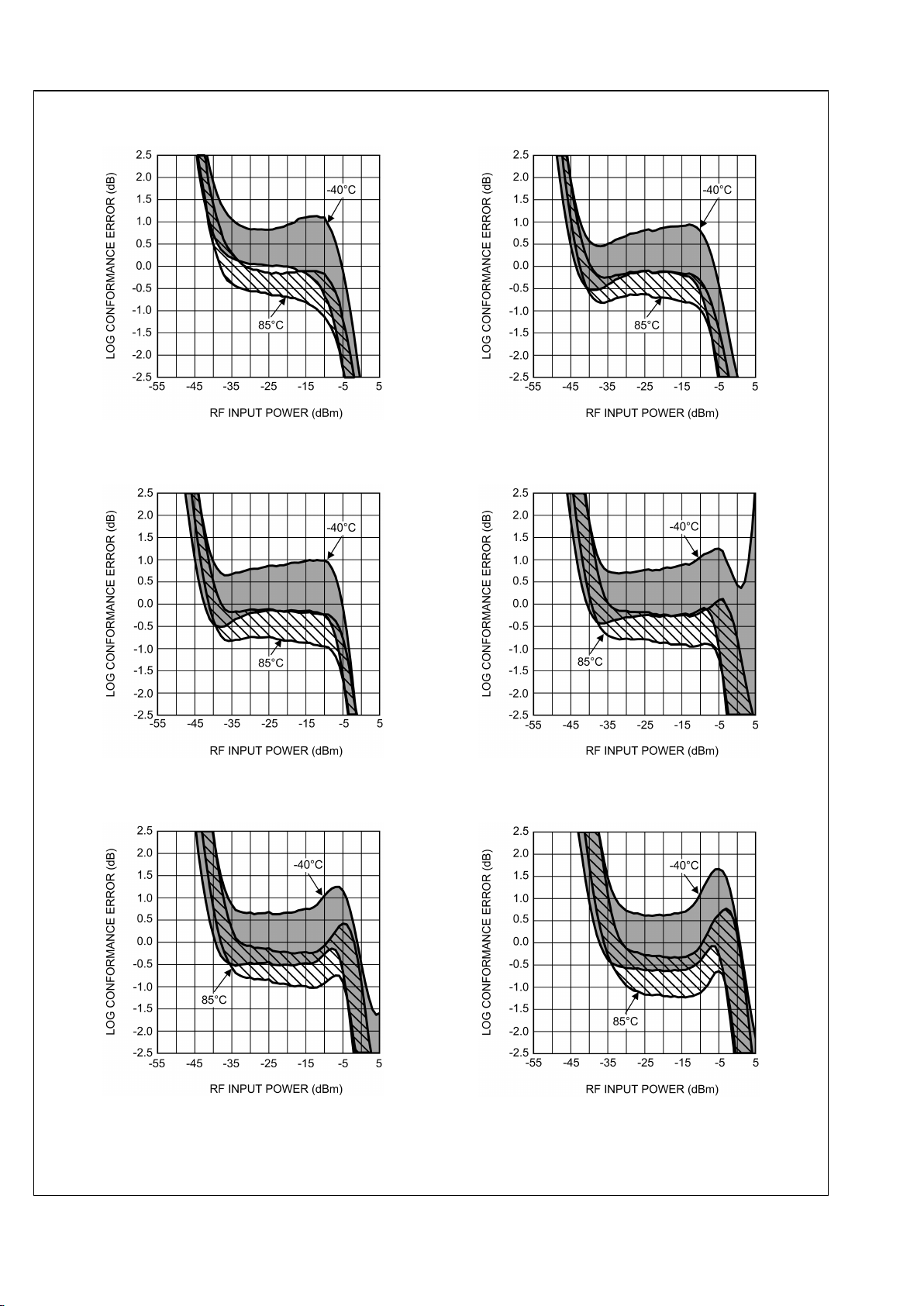
Log Conformance Error (Mean ±3 sigma) vs.
RF Input Power at 50 MHz
20173762
Log Conformance Error (Mean ±3 sigma) vs.
RF Input Power at 900 MHz
20173763
Log Conformance Error (Mean ±3 sigma) vs.
RF Input Power at 1855 MHz
20173764
Log Conformance Error (Mean ±3 sigma) vs.
RF Input Power at 2500 MHz
20173768
Log Conformance Error (Mean ±3 sigma) vs.
RF Input Power at 3000 MHz
20173769
Log Conformance Error (Mean ±3 sigma) vs.
RF Input Power at 3500 MHz
20173767
9 www.national.com
LMV221
Page 10
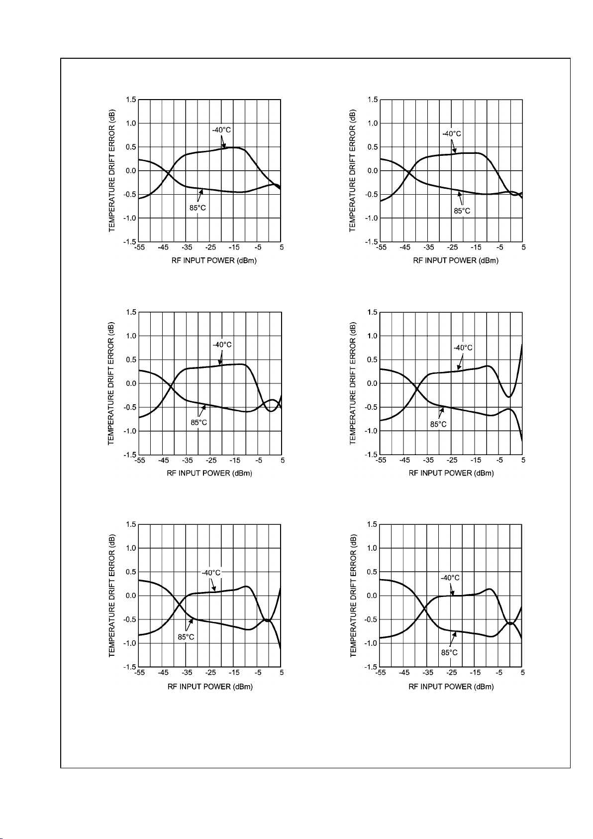
Mean Temperature Drift Error vs.
RF Input Power at 50 MHz
20173720
Mean Temperature Drift Error vs.
RF Input Power at 900 MHz
20173721
Mean Temperature Drift Error vs.
RF Input Power at 1855 MHz
20173722
Mean Temperature Drift Error vs.
RF Input Power at 2500 MHz
20173723
Mean Temperature Drift Error vs.
RF Input Power at 3000 MHz
20173724
Mean Temperature Drift Error vs.
RF Input Power at 3500 MHz
20173725
www.national.com 10
LMV221
Page 11

Temperature Drift Error (Mean ±3 sigma) vs.
RF Input Power at 50 MHz
20173750
Temperature Drift Error (Mean ±3 sigma) vs.
RF Input Power at 900 MHz
20173751
Temperature Drift Error (Mean ±3 sigma) vs.
RF Input Power at 1855 MHz
20173752
Temperature Drift Error (Mean ±3 sigma) vs.
RF Input Power at 2500 MHz
20173753
Temperature Drift Error (Mean ±3 sigma) vs.
RF Input Power at 3000 MHz
20173754
Temperature Drift Error (Mean ±3 sigma) vs.
RF Input Power at 3500 MHz
20173755
11 www.national.com
LMV221
Page 12

Error for 1 dB Input Power Step vs.
RF Input Power at 50 MHz
20173726
Error for 1 dB Input Power Step vs.
RF Input Power at 900 MHz
20173727
Error for 1 dB Input Power Step vs.
RF Input Power at 1855 MHz
20173728
Error for 1 dB Input Power Step vs.
RF Input Power at 2500 MHz
20173729
Error for 1 dB Input Power Step vs.
RF Input Power at 3000 MHz
20173730
Error for 1 dB Input Power Step vs.
RF Input Power at 3500 MHz
20173731
www.national.com 12
LMV221
Page 13

Error for 10 dB Input Power Step vs.
RF Input Power at 50 MHz
20173732
Error for 10 dB Input Power Step vs.
RF Input Power at 900 MHz
20173733
Error for 10 dB Input Power Step vs.
RF Input Power at 1855 MHz
20173734
Error for 10 dB Input Power Step vs.
RF Input Power at 2500 MHz
20173735
Error for 10 dB Input Power Step vs.
RF Input Power at 3000 MHz
20173736
Error for 10 dB Input Power Step vs.
RF Input Power at 3500 MHz
20173737
13 www.national.com
LMV221
Page 14

Mean Temperature Sensitivity vs.
RF Input Power at 50 MHz
20173738
Mean Temperature Sensitivity vs.
RF Input Power at 900 MHz
20173739
Mean Temperature Sensitivity vs.
RF Input Power at 1855 MHz
20173740
Mean Temperature Sensitivity vs.
RF Input Power at 2500 MHz
20173741
Mean Temperature Sensitivity vs.
RF Input Power at 3000 MHz
20173742
Mean Temperature Sensitivity vs.
RF Input Power at 3500 MHz
20173743
www.national.com 14
LMV221
Page 15

Temperature Sensitivity (Mean ±3 sigma) vs.
RF Input Power at 50 MHz
20173756
Temperature Sensitivity (Mean ±3 sigma) vs.
RF Input Power at 900 MHz
20173757
Temperature Sensitivity (Mean ±3 sigma) vs.
RF Input Power at 1855 MHz
20173758
Temperature Sensitivity (Mean ±3 sigma) vs.
RF Input Power at 2500 MHz
20173759
Temperature Sensitivity (Mean ±3 sigma) vs.
RF Input Power at 3000 MHz
20173760
Temperature Sensitivity (Mean ±3 sigma) vs.
RF Input Power at 3500 MHz
20173761
15 www.national.com
LMV221
Page 16

Output Voltage and Log Conformance Error vs.
RF Input Power for various modulation types at 900 MHz
20173772
Output Voltage and Log Conformance Error vs.
RF Input Power for various modulation types at 1855 MHz
20173773
RF Input Impedance vs. Frequency
(Resistance & Reactance)
20173748
Output Noise Spectrum vs. Frequency
20173745
Power Supply Rejection Ratio vs. Frequency
20173747
Output Amplifier Gain & Phase vs. Frequency
20173707
www.national.com 16
LMV221
Page 17

Sourcing Output Current vs. Output Voltage
20173709
Sinking Output Current vs. Output Voltage
20173710
Output Voltage vs. Sourcing Current
20173711
Output Voltage vs. Sinking Current
20173706
17 www.national.com
LMV221
Page 18

Application Notes
The LMV221 is a versatile logarithmic RF power detector
suitable for use in power measurement systems. The
LMV221 is particularly well suited for CDMA and UMTS applications. It produces a DC voltage that is a measure for the
applied RF power.
This application section describes the behavior of the
LMV221 and explains how accurate measurements can be
performed. Besides this an overview is given of the interfacing
options with the connected circuitry as well as the recommended layout for the LMV221.
1. FUNCTIONALITY AND APPLICATION OF RF POWER
DETECTORS
This first section describes the functional behavior of RF power detectors and their typical application. Based on a number
of key electrical characteristics of RF power detectors, section
1.1 discusses the functionality of RF power detectors in general and of the LMV221 LOG detector in particular. Subsequently, section 1.2 describes two important applications of
the LMV221 detector.
1.1 Functionality of RF Power Detectors
An RF power detector is a device that produces a DC output
voltage in response to the RF power level of the signal applied
to its input. A wide variety of power detectors can be distinguished, each having certain properties that suit a particular
application. This section provides an overview of the key
characteristics of power detectors, and discusses the most
important types of power detectors. The functional behavior
of the LMV221 is discussed in detail.
1.1.1 Key Characteristics of RF Power Detectors.
Power detectors are used to accurately measure the power
of a signal inside the application. The attainable accuracy of
the measurement is therefore dependent upon the accuracy
and predictability of the detector transfer function from the RF
input power to the DC output voltage.
Certain key characteristics determine the accuracy of RF detectors and they are classified accordingly:
•
Temperature Stability
•
Dynamic Range
•
Waveform Dependency
•
Transfer Shape
Each of these aspects is discussed in further detail below.
Generally, the transfer function of RF power detectors is
slightly temperature dependent. This temperature drift re-
duces the accuracy of the power measurement, because
most applications are calibrated at room temperature. In such
systems, the temperature drift significantly contributes to the
overall system power measurement error. The temperature
stability of the transfer function differs for the various types of
power detectors. Generally, power detectors that contain only
one or few semiconductor devices (diodes, transistors) operating at RF frequencies attain the best temperature stability.
The dynamic range of a power detector is the input power
range for which it creates an accurately reproducible output
signal. What is considered accurate is determined by the applied criterion for the detector accuracy; the detector dynamic
range is thus always associated with certain power measurement accuracy. This accuracy is usually expressed as the
deviation of its transfer function from a certain predefined relationship, such as ”linear in dB" for LOG detectors and
”square-law" transfer (from input RF voltage to DC output
voltage) for Mean-Square detectors. For LOG-detectors, the
dynamic range is often specified as the power range for which
its transfer function follows the ideal linear-in-dB relationship
with an error smaller than or equal to ±1 dB. Again, the attainable dynamic range differs considerably for the various
types of power detectors.
According to its definition, the average power is a metric for
the average energy content of a signal and is not directly a
function of the shape of the signal in time. In other words, the
power contained in a 0 dBm sine wave is identical to the power contained in a 0 dBm square wave or a 0 dBm WCDMA
signal; all these signals have the same average power. Depending on the internal detection mechanism, though, power
detectors may produce a slightly different output signal in response to the aforementioned waveforms, even though their
average power level is the same. This is due to the fact that
not all power detectors strictly implement the definition formula for signal power, being the mean of the square of the
signal. Most types of detectors perform some mixture of peak
detection and average power detection. A waveform independent detector response is often desired in applications
that exhibit a large variety of waveforms, such that separate
calibration for each waveform becomes impractical.
The shape of the detector transfer function from the RF input
power to the DC output voltage determines the required resolution of the ADC connected to it. The overall power measurement error is the combination of the error introduced by
the detector, and the quantization error contributed by the
ADC. The impact of the quantization error on the overall
transfer's accuracy is highly dependent on the detector transfer shape, as illustrated in Figure 1.
www.national.com 18
LMV221
Page 19

20173770
(a)
20173766
(b)
FIGURE 1. Convex Detector Transfer Function (a) and Linear Transfer Function (b)
Figure 1 shows two different representations of the detector
transfer function. In both graphs the input power along the
horizontal axis is displayed in dBm, since most applications
specify power accuracy requirements in dBm (or dB). The
figure on the left shows a convex detector transfer function,
while the transfer function on the right hand side is linear (in
dB). The slope of the detector transfer function — i.e. the detector conversion gain – is of key importance for the impact
of the quantization error on the total measurement error. If the
detector transfer function slope is low, a change, ΔP, in the
input power results only in a small change of the detector output voltage, such that the quantization error will be relatively
large. On the other hand, if the detector transfer function slope
is high, the output voltage change for the same input power
change will be large, such that the quantization error is small.
The transfer function on the left has a very low slope at low
input power levels, resulting in a relatively large quantization
error. Therefore, to achieve accurate power measurement in
this region, a high-resolution ADC is required. On the other
hand, for high input power levels the quantization error will be
very small due to the steep slope of the curve in this region.
For accurate power measurement in this region, a much lower
ADC resolution is sufficient. The curve on the right has a constant slope over the power range of interest, such that the
required ADC resolution for a certain measurement accuracy
is constant. For this reason, the LOG-linear curve on the right
will generally lead to the lowest ADC resolution requirements
for certain power measurement accuracy.
1.1.2 Types of RF Power Detectors
Three different detector types are distinguished based on the
four characteristics previously discussed:
•
Diode Detector
•
(Root) Mean Square Detector
•
Logarithmic Detector
These three types of detectors are discussed in the following
sections. Advantages and disadvantages will be presented
for each type.
Diode Detector
A diode is one of the simplest types of RF detectors. As depicted in Figure 2, the diode converts the RF input voltage into
a rectified current. This unidirectional current charges the capacitor. The RC time constant of the resistor and the capacitor
determines the amount of filtering applied to the rectified (detected) signal.
20173774
FIGURE 2. Diode Detector
The advantages and disadvantages can be summarized as
follows:
•
The temperature stability of the diode detectors is
generally very good, since they contain only one
semiconductor device that operates at RF frequencies.
•
The dynamic range of diode detectors is poor. The
conversion gain from the RF input power to the output
voltage quickly drops to very low levels when the input
power decreases. Typically a dynamic range of 20 – 25 dB
can be realized with this type of detector.
•
The response of diode detectors is waveform dependent.
As a consequence of this dependency its output voltage
for e.g. a 0 dBm WCDMA signal is different than for a
0 dBm unmodulated carrier. This is due to the fact that the
diode measures peak power instead of average power.
The relation between peak power and average power is
dependent on the wave shape.
•
The transfer shape of diode detectors puts high
requirements on the resolution of the ADC that reads their
output voltage. Especially at low input power levels a very
high ADC resolution is required to achieve sufficient power
measurement accuracy (See Figure 1, left side).
(Root) Mean Square Detector
This type of detector is particularly suited for the power measurements of RF modulated signals that exhibits large peak
to average power ratio variations. This is because its opera-
19 www.national.com
LMV221
Page 20

tion is based on direct determination of the average power
and not – like the diode detector – of the peak power.
The advantages and disadvantages can be summarized as
follows:
•
The temperature stability of (R)MS detectors is almost as
good as the temperature stability of the diode detector;
only a small part of the circuit operates at RF frequencies,
while the rest of the circuit operates at low frequencies.
•
The dynamic range of (R)MS detectors is limited. The
lower end of the dynamic range is limited by internal device
offsets.
•
The response of (R)MS detectors is highly waveform
independent. This is a key advantage compared to other
types of detectors in applications that employ signals with
high peak-to-average power variations. For example, the
(R)MS detector response to a 0 dBm WCDMA signal and
a 0 dBm unmodulated carrier is essentially equal.
•
The transfer shape of R(MS) detectors has many
similarities with the diode detector and is therefore subject
to similar disadvantages with respect to the ADC
resolution requirements (See Figure 1, left side).
Logarithmic Detectors
The transfer function of a logarithmic detector has a linear in
dB response, which means that the output voltage changes
linearly with the RF power in dBm. This is convenient since
most communication standards specify transmit power levels
in dBm as well.
The advantages and disadvantages can be summarized as
follows:
•
The temperature stability of the LOG detector transfer
function is generally not as good as the stability of diode
and R(MS) detectors. This is because a significant part of
the circuit operates at RF frequencies.
•
The dynamic range of LOG detectors is usually much
larger than that of other types of detectors.
•
Since LOG detectors perform a kind of peak detection their
response is wave form dependent, similar to diode
detectors.
•
The transfer shape of LOG detectors puts the lowest
possible requirements on the ADC resolution (See Figure
1, right side).
1.1.3 Characteristics of the LMV221
The LMV221 is a Logarithmic RF power detector with approximately 40 dB dynamic range. This dynamic range plus
its logarithmic behavior make the LMV221 ideal for various
applications such as wireless transmit power control for CDMA and UMTS applications. The frequency range of the
LMV221 is from 50 MHz to 3.5 GHz, which makes it suitable
for various applications.
The LMV221 transfer function is accurately temperature compensated. This makes the measurement accurate for a wide
temperature range. Furthermore, the LMV221 can easily be
connected to a directional coupler because of its 50 ohm input
termination. The output range is adjustable to fit the ADC input
range. The detector can be switched into a power saving
shutdown mode for use in pulsed conditions.
1.2 Applications of RF Power Detectors
RF power detectors can be used in a wide variety of applications. This section discusses two application. The first example shows the LMV221 in a transmit power control loop, the
second application measures the voltage standing wave ratio
(VSWR).
1.2.1 Transmit Power Control Loop
The key benefit of a transmit power control loop circuit is that
it makes the transmit power insensitive to changes in the
Power Amplifier (PA) gain control function, such as changes
due to temperature drift. When a control loop is used, the
transfer function of the PA is eliminated from the overall transfer function. Instead, the overall transfer function is determined by the power detector. The overall transfer function
accuracy depends thus on the RF detector accuracy. The
LMV221 is especially suited for this application, due to the
accurate temperature stability of its transfer function.
Figure 3 shows a block diagram of a typical transmit power
control system. The output power of the PA is measured by
the LMV221 through a directional coupler. The measured
output voltage of the LMV221 is filtered and subsequently
digitized by the ADC inside the baseband chip. The baseband
adjusts the PA output power level by changing the gain control
signal of the RF VGA accordingly. With an input impedance
of 50Ω, the LMV221 can be directly connected to a 30 dB
directional coupler without the need for an additional external
attenuator. The setup can be adjusted to various PA output
ranges by selection of a directional coupler with the appropriate coupling factor.
20173797
FIGURE 3. Transmit Power Control System
1.2.2 Voltage Standing Wave Ratio Measurement
Transmission in RF systems requires matched termination by
the proper characteristic impedance at the transmitter and
receiver side of the link. In wireless transmission systems
though, matched termination of the antenna can rarely be
achieved. The part of the transmitted power that is reflected
at the antenna bounces back toward the PA and may cause
standing waves in the transmission line between the PA and
the antenna. These standing waves can attain unacceptable
levels that may damage the PA. A Voltage Standing Wave
Ratio (VSWR) measurement is used to detect such an occasion. It acts as an alarm function to prevent damage to the
transmitter.
VSWR is defined as the ratio of the maximum voltage divided
by the minimum voltage at a certain point on the transmission
line:
Where Γ = V
REFLECTED
/ V
FORWARD
denotes the reflection co-
efficient.
This means that to determine the VSWR, both the forward
(transmitted) and the reflected power levels have to be mea-
www.national.com 20
LMV221
Page 21

sured. This can be accomplished by using two LMV221 RF
power detectors according to Figure 4. A directional coupler
is used to separate the forward and reflected power waves on
the transmission line between the PA and the antenna. One
secondary output of the coupler provides a signal proportional
to the forward power wave, the other secondary output provides a signal proportional to the reflected power wave. The
outputs of both RF detectors that measure these signals are
connected to a micro-controller or baseband that calculates
the VSWR from the detector output signals.
20173794
FIGURE 4. VSWR Application
2. ACCURATE POWER MEASUREMENT
The power measurement accuracy achieved with a power
detector is not only determined by the accuracy of the detector
itself, but also by the way it is integrated into the application.
In many applications some form of calibration is employed to
improve the accuracy of the overall system beyond the intrinsic accuracy provided by the power detector. For example, for
LOG-detectors calibration can be used to eliminate part to
part spread of the LOG-slope and LOG-intercept from the
overall power measurement system, thereby improving its
power measurement accuracy.
This section shows how calibration techniques can be used
to improve the accuracy of a power measurement system beyond the intrinsic accuracy of the power detector itself. The
main focus of the section is on power measurement systems
using LOG-detectors, specifically the LMV221, but the more
generic concepts can also be applied to other power detectors. Other factors influencing the power measurement accuracy, such as the resolution of the ADC reading the detector
output signal will not be considered here since they are not
fundamentally due to the power detector.
2.1 Concept of Power Measurements
Power measurement systems generally consists of two clearly distinguishable parts with different functions:
1.
A power detector device, that generates a DC output
signal (voltage) in response to the power level of the (RF)
signal applied to its input.
2.
An “estimator” that converts the measured detector
output signal into a (digital) numeric value representing
the power level of the signal at the detector input.
A sketch of this conceptual configuration is depicted in Figure
5 .
20173779
FIGURE 5. Generic Concept of a Power Measurement
System
The core of the estimator is usually implemented as a software algorithm, receiving a digitized version of the detector
output voltage. Its transfer F
EST
from detector output voltage
to a numerical output should be equal to the inverse of the
detector transfer F
DET
from (RF) input power to DC output
voltage. If the power measurement system is ideal, i.e. if no
errors are introduced into the measurement result by the detector or the estimator, the measured power P
EST
- the output
of the estimator - and the actual input power PIN should be
identical. In that case, the measurement error E, the difference between the two, should be identically zero:
From the expression above it follows that one would design
the F
EST
transfer function to be the inverse of the F
DET
transfer
function.
In practice the power measurement error will not be zero, due
to the following effects:
•
The detector transfer function is subject to various kinds
of random errors that result in uncertainty in the detector
output voltage; the detector transfer function is not exactly
known.
•
The detector transfer function might be too complicated to
be implemented in a practical estimator.
The function of the estimator is then to estimate the input
power PIN, i.e. to produce an output P
EST
such that the power
measurement error is - on average - minimized, based on the
following information:
1.
Measurement of the not completely accurate detector
output voltage V
OUT
2.
Knowledge about the detector transfer function F
DET
, for
example the shape of the transfer function, the types of
errors present (part-to-part spread, temperature drift) etc.
Obviously the total measurement accuracy can be optimized
by minimizing the uncertainty in the detector output signal (i.e.
select an accurate power detector), and by incorporating as
much accurate information about the detector transfer function into the estimator as possible.
The knowledge about the detector transfer function is condensed into a mathematical model for the detector transfer
function, consisting of:
•
A formula for the detector transfer function.
21 www.national.com
LMV221
Page 22

•
Values for the parameters in this formula.
The values for the parameters in the model can be obtained
in various ways. They can be based on measurements of the
detector transfer function in a precisely controlled environment (parameter extraction). If the parameter values are separately determined for each individual device, errors like partto-part spread are eliminated from the measurement system.
Obviously, errors may occur when the operating conditions of
the detector (e.g. the temperature) become significantly different from the operating conditions during calibration (e.g.
room temperature). Subsequent sections will discuss examples of simple estimators for power measurements that result
in a number of commonly used metrics for the power measurement error: the LOG-conformance error, the temperature
drift error, the temperature sensitivity and differential power
error.
2.2 LOG-Conformance Error
Probably the simplest power measurement system that can
be realized is obtained when the LOG-detector transfer function is modelled as a perfect linear-in-dB relationship between
the input power and output voltage:
in which K
SLOPE
represents the LOG-slope and P
INTERCEPT
the
LOG-intercept. The estimator based on this model implements the inverse of the model equation, i.e.
The resulting power measurement error, the LOG-conformance error, is thus equal to:
The most important contributions to the LOG-conformance
error are generally:
•
The deviation of the actual detector transfer function from
an ideal Logarithm (the transfer function is nonlinear in
dB).
•
Drift of the detector transfer function over various
environmental conditions, most importantly temperature;
K
SLOPE
and P
INTERCEPT
are usually determined for room
temperature only.
•
Part-to-part spread of the (room temperature) transfer
function.
The latter component is conveniently removed by means of
calibration, i.e. if the LOG slope and LOG-intercept are determined for each individual detector device (at room temperature). This can be achieved by measurement of the detector
output voltage - at room temperature - for a series of different
power levels in the LOG-linear range of the detector transfer
function. The slope and intercept can then be determined by
means of linear regression.
An example of this type of error and its relationship to the
detector transfer function is depicted in Figure 6.
20173715
FIGURE 6. LOG-Conformance Error and LOG-Detector
Transfer Function
In the center of the detector's dynamic range, the LOG-conformance error is small, especially at room temperature; in
this region the transfer function closely follows the linear-indB relationship while K
SLOPE
and P
INTERCEPT
are determined
based on room temperature measurements. At the temperature extremes the error in the center of the range is slightly
larger due to the temperature drift of the detector transfer
function. The error rapidly increases toward the top and bottom end of the detector's dynamic range; here the detector
saturates and its transfer function starts to deviate significantly from the ideal LOG-linear model. The detector dynamic
range is usually defined as the power range for which the LOG
conformance error is smaller than a specified amount. Often
an error of ±1 dB is used as a criterion.
2.3 Temperature Drift Error
A more accurate power measurement system can be obtained if the first error contribution, due to the deviation from
the ideal LOG-linear model, is eliminated. This is achieved if
the actual measured detector transfer function at room temperature is used as a model for the detector, instead of the
ideal LOG-linear transfer function used in the previous section.
The formula used for such a detector is:
V
OUT,MOD
= F
DET(PIN,TO
)
where TO represents the temperature during calibration (room
temperature). The transfer function of the corresponding estimator is thus the inverse of this:
In this expression V
OUT
(T) represents the measured detector
output voltage at the operating temperature T.
The resulting measurement error is only due to drift of the
detector transfer function over temperature, and can be expressed as:
www.national.com 22
LMV221
Page 23

Unfortunately, the (numeric) inverse of the detector transfer
function at different temperatures makes this expression
rather impractical. However, since the drift error is usually
small V
OUT
(T) is only slightly different from V
OUT(TO
). This
means that we can apply the following approximation:
This expression is easily simplified by taking the following
considerations into account:
•
The drift error at the calibration temperature E(TO,TO)
equals zero (by definition).
•
The estimator transfer F
DET(VOUT,TO
) is not a function of
temperature; the estimator output changes over
temperature only due to the temperature dependence of
V
OUT
.
•
The actual detector input power PIN is not temperature
dependent (in the context of this expression).
•
The derivative of the estimator transfer function to V
OUT
equals approximately 1/K
SLOPE
in the LOG-linear region of
the detector transfer function (the region of interest).
Using this, we arrive at:
This expression is very similar to the expression of the LOGconformance error determined previously. The only difference is that instead of the output of the ideal LOG-linear
model, the actual detector output voltage at the calibration
temperature is now subtracted from the detector output voltage at the operating temperature.
Figure 7 depicts an example of the drift error.
20173722
FIGURE 7. Temperature Drift Error of the LMV221
at f = 1855 MHz
In agreement with the definition, the temperature drift error is
zero at the calibration temperature. Further, the main difference with the LOG-conformance error is observed at the top
and bottom end of the detection range; instead of a rapid increase the drift error settles to a small value at high and low
input power levels due to the fact that the detector saturation
levels are relatively temperature independent.
In a practical application it may not be possible to use the
exact inverse detector transfer function as the algorithm for
the estimator. For example it may require too much memory
and/or too much factory calibration time. However, using the
ideal LOG-linear model in combination with a few extra data
points at the top and bottom end of the detection range where the deviation is largest - can already significantly reduce the power measurement error.
2.4 Temperature Compensation
A further reduction of the power measurement error is possible if the operating temperature is measured in the application. For this purpose, the detector model used by the
estimator should be extended to cover the temperature dependency of the detector.
Since the detector transfer function is generally a smooth
function of temperature (the output voltage changes gradually
over temperature), the temperature is in most cases adequately modeled by a first-order or second-order polynomial,
i.e.
The required temperature dependence of the estimator, to
compensate for the detector temperature dependence can be
approximated similarly:
The last approximation results from the fact that a first-order
temperature compensation is usually sufficiently accurate.
The remainder of this section will therefore concentrate on
first-order compensation. For second and higher-order compensation a similar approach can be followed.
Ideally, the temperature drift could be completely eliminated
if the measurement system is calibrated at various temperatures and input power levels to determine the Temperature
Sensitivity S1. In a practical application, however that is usually not possible due to the associated high costs. The alternative is to use the average temperature drift in the estimator,
instead of the temperature sensitivity of each device individually. In this way it becomes possible to eliminate the systematic (reproducible) component of the temperature drift
without the need for calibration at different temperatures during manufacturing. What remains is the random temperature
drift, which differs from device to device. Figure 8 illustrates
the idea. The graph at the left schematically represents the
behavior of the drift error versus temperature at a certain input
power level for a large number of devices.
23 www.national.com
LMV221
Page 24

20173765
FIGURE 8. Elimination of the Systematic Component from the Temperature Drift
The mean drift error represents the reproducible - systematic
- part of the error, while the mean ± 3 sigma limits represent
the combined systematic plus random error component. Obviously the drift error must be zero at calibration temperature
T0. If the systematic component of the drift error is included
in the estimator, the total drift error becomes equal to only the
random component, as illustrated in the graph at the right of
Figure 8. A significant reduction of the temperature drift error
can be achieved in this way only if:
•
The systematic component is significantly larger than the
random error component (otherwise the difference is
negligible).
•
The operating temperature is measured with sufficient
accuracy.
It is essential for the effectiveness of the temperature compensation to assign the appropriate value to the temperature
sensitivity S1. Two different approaches can be followed to
determine this parameter:
•
Determination of a single value to be used over the entire
operating temperature range.
•
Division of the operating temperature range in segments
and use of separate values for each of the segments.
Also for the first method, the accuracy of the extracted temperature sensitivity increases when the number of measure-
ment temperatures increases. Linear regression to temperature can then be used to determine the two parameters of the
linear model for the temperature drift error: the first order temperature sensitivity S1 and the best-fit (room temperature)
value for the power estimate at T0 :F
DET[VOUT
(T),T0]. Note that
to achieve an overall - over all temperatures - minimum error,
the room temperature drift error in the model can be non-zero
at the calibration temperature (which is not in agreement with
the strict definition).
The second method does not have this drawback but is more
complex. In fact, segmentation of the temperature range is a
form of higher-order temperature compensation using only a
first-order model for the different segments: one for temperatures below 25°C, and one for temperatures above 25°C.
The mean (or typical) temperature sensitivity is the value to
be used for compensation of the systematic drift error component. Figure 9 shows the temperature drift error without and
with temperature compensation using two segments. With
compensation the systematic component is completely eliminated; the remaining random error component is centered
around zero. Note that the random component is slightly larger at −40°C than at 85°C.
20173752
20173795
FIGURE 9. Temperature Drift Error without and with Temperature Compensation
www.national.com 24
LMV221
Page 25

In a practical power measurement system, temperature compensation is usually only applied to a small power range
around the maximum power level for two reasons:
•
The various communication standards require the highest
accuracy in this range to limit interference.
•
The temperature sensitivity itself is a function of the power
level it becomes impractical to store a large number of
different temperature sensitivity values for different power
levels.
The table in the datasheet specifies the temperature sensitivity for the aforementioned two segments at an input power
level of -10 dBm (near the top-end of the detector dynamic
range). The typical value represents the mean which is to be
used for calibration.
2.5 Differential Power Errors
Many third generation communication systems contain a
power control loop through the base station and mobile unit
that requests both to frequently update the transmit power
level by a small amount (typically 1 dB). For such applications
it is important that the actual change of the transmit power is
sufficiently close to the requested power change.
The error metrics in the datasheet that describe the accuracy
of the detector for a change in the input power are E
1 dB
(for
a 1 dB change in the input power) and E
10 dB
(for a 10 dB step,
or ten consecutive steps of 1 dB). Since it can be assumed
that the temperature does not change during the power step
the differential error equals the difference of the drift error at
the two involved power levels:
It should be noted that the step error increases significantly
when one (or both) power levels in the above expression are
outside the detector dynamic range. For E
10 dB
this occurs
when PIN is less than 10 dB below the maximum input power
of the dynamic range, P
MAX
.
3. DETECTOR INTERFACING
For optimal performance of the LMV221, it is important that
all its pins are connected to the surrounding circuitry in the
appropriate way. This section discusses guidelines and requirements for the electrical connection of each pin of the
LMV221 to ensure proper operation of the device. Starting
from a block diagram, the function of each pin is elaborated.
Subsequently, the details of the electrical interfacing are separately discussed for each pin. Special attention will be paid
to the output filtering options and the differences between
single ended and differential interfacing with an ADC.
3.1 Block Diagram of the LMV221
The block diagram of the LMV221 is depicted in Figure 10.
20173703
FIGURE 10. Block Diagram of the LMV221
The core of the LMV221 is a progressive compression LOGdetector consisting of four gain stages. Each of these saturating stages has a gain of approximately 10 dB and therefore
realizes about 10 dB of the detector dynamic range. The five
diode cells perform the actual detection and convert the RF
signal to a DC current. This DC current is subsequently supplied to the transimpedance amplifier at the output, that converts it into an output voltage. In addition, the amplifier
provides buffering of and applies filtering to the detector output signal. To prevent discharge of filtering capacitors between OUT and GND in shutdown, a switch is inserted at the
amplifier input that opens in shutdown to realize a high
impedance output of the device.
3.2 RF Input
RF parts typically use a characteristic impedance of 50Ω. To
comply with this standard the LMV221 has an input
impedance of 50Ω. Using a characteristic impedance other
then 50Ω will cause a shift of the logarithmic intercept with
respect to the value given in the electrical characteristics table. This intercept shift can be calculated according to the
following formula: .
The intercept will shift to higher power levels for
R
SOURCE
> 50Ω, and will shift to lower power levels for
R
SOURCE
< 50Ω.
3.3 Shutdown
To save power, the LMV221 can be brought into a low-power
shutdown mode. The device is active for EN = HIGH
(VEN>1.1V) and in the low-power shutdown mode for EN =
LOW (VEN < 0.6V). In this state the output of the LMV221 is
switched to a high impedance mode. Using the shutdown
25 www.national.com
LMV221
Page 26

function, care must be taken not to exceed the absolute maximum ratings. Forcing a voltage to the enable input that is 400
mV higher than VDD or 400 mV lower than GND will damage
the device and further operations is not guaranteed. The absolute maximum ratings can also be exceeded when the
enable EN is switched to HIGH (from shutdown to active
mode) while the supply voltage is low (off). This should be
prevented at all times. A possible solution to protect the part
is to add a resistor of 100 kΩ in series with the enable input.
3.4 Output and Reference
This section describes the possible filtering techniques that
can be applied to reduce ripple in the detector output voltage.
In addition two different topologies to connect the LMV221 to
an ADC are elaborated.
3.4.1 Filtering
The output voltage of the LMV221 is a measure for the applied
RF signal on the RF input pin. Usually, the applied RF signal
contains AM modulation that causes low frequency ripple in
the detector output voltage. CDMA signals for instance contain a large amount of amplitude variations. Filtering of the
output signal can be used to eliminate this ripple. The filtering
can either be realized by a low pass output filter or a low pass
feedback filter. Those two techniques are depicted in Figure
11.
20173775 20173776
FIGURE 11. Low Pass Output Filter and Low Pass Feedback Filter
Depending on the system requirements one of the these filtering techniques can be selected. The low pass output filter
has the advantage that it preserves the output voltage when
the LMV221 is brought into shutdown. This is elaborated in
section 3.4.3. In the feedback filter, resistor RP discharges
capacitor CP in shutdown and therefore changes the output
voltage of the device.
A disadvantage of the low pass output filter is that the series
resistor RS limits the output drive capability. This may cause
inaccuracies in the voltage read by an ADC when the ADC
input impedance is not significantly larger than RS. In that
case, the current flowing through the ADC input induces an
error voltage across filter resistor RS. The low pass feedback
filter doesn’t have this disadvantage.
Note that adding an external resistor between OUT and REF
reduces the transfer gain (LOG-slope and LOG-intercept) of
the device. The internal feedback resistor sets the gain of the
transimpedance amplifier.
The filtering of the low pass output filter is realized by resistor
RS and capacitor CS. The −3 dB bandwidth of this filter can
then be calculated by: f
−3 dB
= 1 / 2πRSCS. The bandwidth of
the low pass feedback filter is determined by external resistor
RP in parallel with the internal resistor R
TRANS
, and external
capacitor CP in parallel with internal capacitor C
TRANS
(see
Figure 13). The −3 dB bandwidth of the feedback filter can be
calculated by f
−3 dB
= 1 / 2π (RP//R
TRANS
) (CP+C
TRANS
). The
bandwidth set by the internal resistor and capacitor (when no
external components are connected between OUT and REF)
equals f
−3 dB
= 1 / 2π R
TRANS CTRANS
= 450 kHz.
3.4.2 Interface to the ADC
The LMV221 can be connected to the ADC with a single ended or a differential topology. The single ended topology connects the output of the LMV221 to the input of the ADC and
the reference pin is not connected. In a differential topology,
both the output and the reference pins of the LMV221 are
connected to the ADC. The topologies are depicted in Figure
12.
20173776 20173777
FIGURE 12. Single Ended and Differential Application
www.national.com 26
LMV221
Page 27

The differential topology has the advantage that it is compensated for temperature drift of the internal reference voltage.
This can be explained by looking at the transimpedance amplifier of the LMV221 (Figure 13).
20173778
FIGURE 13. Output Stage of the LMV221
It can be seen that the output of the amplifier is set by the
detection current I
DET
multiplied by the resistor R
TRANS
plus
the reference voltage V
REF
:
V
OUT
= I
DET RTRANS
+ V
REF
I
DET
represents the detector current that is proportional to the
RF input power. The equation shows that temperature variations in V
REF
are also present in the output V
OUT
. In case of a
single ended topology the output is the only pin that is connected to the ADC. The ADC voltage for single ended is thus:
Single ended: V
ADC
= I
DET RTRANS
+ V
REF
A differential topology also connects the reference pin, which
is the value of reference voltage V
REF
. The ADC reads V
OUT
- V
REF
:
Differential: V
ADC
= V
OUT
- V
REF
= I
DET RTRANS
The resulting equation doesn’t contain the reference voltage
V
REF
anymore. Temperature variations in this reference volt-
age are therefore not measured by the ADC.
3.4.3 Output Behavior in Shutdown
In order to save power, the LMV221 can be used in pulsed
mode, such that it is active to perform the power measurement only during a fraction of the time. During the remaining
time the device is in low-power shutdown. Applications using
this approach usually require that the output value is available
at all times, also when the LMV221 is in shutdown. The settling time in active mode, however, should not become excessively large. This can be realized by the combination of
the LMV221 and a low pass output filter (see Figure 11, left
side), as discussed below.
In active mode, the filter capacitor CS is charged to the output
voltage of the LMV221 — which in this mode has a low output
impedance to enable fast settling. During shutdown-mode,
the capacitor should preserve this voltage. Discharge of C
S
through any current path should therefore be avoided in shutdown. The output impedance of the LMV221 becomes high
in shutdown, such that the discharge current cannot flow from
the capacitor top plate, through RS, and the LMV221's OUT
pin to GND. This is realized by the internal shutdown mechanism of the output amplifier and by the switch depicted in
Figure 13. Additionally, it should be ensured that the ADC input impedance is high as well, to prevent a possible discharge
path through the ADC.
4. BOARD LAYOUT RECOMMENDATIONS
As with any other RF device, careful attention must me paid
to the board layout. If the board layout isn’t properly designed,
unwanted signals can easily be detected or interference will
be picked up. This section gives guidelines for proper board
layout for the LMV221.
Electrical signals (voltages / currents) need a finite time to
travel through a trace or transmission line. RF voltage levels
at the generator side and at the detector side can therefore
be different. This is not only true for the RF strip line, but for
all traces on the PCB. Signals at different locations or traces
on the PCB will be in a different phase of the RF frequency
cycle. Phase differences in, e.g. the voltage across neighboring lines, may result in crosstalk between lines, due to parasitic capacitive or inductive coupling. This crosstalk is further
enhanced by the fact that all traces on the PCB are susceptible to resonance. The resonance frequency depends on the
trace geometry. Traces are particularly sensitive to interference when the length of the trace corresponds to a quarter of
the wavelength of the interfering signal or a multiple thereof.
4.1 Supply Lines
Since the PSRR of the LMV221 is finite, variations of the supply can result in some variation at the output. This can be
caused among others by RF injection from other parts of the
circuitry or the on/off switching of the PA.
4.1.1 Positive Supply (VDD)
In order to minimize the injection of RF interference into the
LMV221 through the supply lines, the phase difference between the PCB traces connecting to VDD and GND should be
minimized. A suitable way to achieve this is to short both connections for RF. This can be done by placing a small decoupling capacitor between the VDD and GND. It should be placed
as close as possible to the VDD and GND pins of the LMV221.
Due to the presence of the RF input, the best possible position
would be to extend the GND plane connecting to the DAP
slightly beyond the short edge of the package, such that the
capacitor can be placed directly to the VDD pin (Figure 14). Be
aware that the resonance frequency of the capacitor itself
should be above the highest RF frequency used in the application, since the capacitor acts as an inductor above its
resonance frequency.
27 www.national.com
LMV221
Page 28

20173701
FIGURE 14. Recommended Board Layout
Low frequency supply voltage variations due to PA switching
might result in a ripple at the output voltage. The LMV221 has
a Power Supply Rejection Ration of 60 dB for low frequencies.
4.1.2 Ground (GND)
The LMV221 needs a ground plane free of noise and other
disturbing signals. It is important to separate the RF ground
return path from the other grounds. This is due to the fact that
the RF input handles large voltage swings. A power level of
0 dBm will cause a voltage swing larger than 0.6 VPP, over the
internal 50Ω input resistor. This will result in a significant RF
return current toward the source. It is therefore recommended
that the RF ground return path not be used for other circuits
in the design. The RF path should be routed directly back to
the source without loops.
4.2 RF Input Interface
The LMV221 is designed to be used in RF applications, having a characteristic impedance of 50Ω. To achieve this
impedance, the input of the LMV221 needs to be connected
via a 50Ω transmission line. Transmission lines can be easily
created on PCBs using microstrip or (grounded) coplanar
waveguide (GCPW) configurations. This section will discuss
both configurations in a general way. For more details about
designing microstrip or GCPW transmission lines, a microwave designer handbook is recommended.
4.2.1 Microstrip Configuration
One way to create a transmission line is to use a microstrip
configuration. A cross section of the configuration is shown in
Figure 15, assuming a two layer PCB.
20173780
FIGURE 15. Microstrip Configuration
A conductor (trace) is placed on the topside of a PCB. The
bottom side of the PCB has a fully copper ground plane. The
characteristic impedance of the microstrip transmission line
is a function of the width W, height H, and the dielectric constant εr.
Characteristics such as height and the dielectric constant of
the board have significant impact on transmission line dimensions. A 50Ω transmission line may result in impractically wide
traces. A typical 1.6 mm thick FR4 board results in a trace
width of 2.9 mm, for instance. This is impractical for the
LMV221, since the pad width of the LLP-6 package is 0.25
mm. The transmission line has to be tapered from 2.9 mm to
0.25 mm. Significant reflections and resonances in the frequency transfer function of the board may occur due to this
tapering.
4.2.2 GCPW Configuration
A transmission line in a (grounded) coplanar waveguide
(GCPW) configuration will give more flexibility in terms of
trace width. The GCPW configuration is constructed with a
conductor surrounded by ground at a certain distance, S, on
the top side. Figure 16 shows a cross section of this configuration. The bottom side of the PCB is a ground plane. The
ground planes on both sides of the PCB should be firmly connected to each other by multiple vias. The characteristic
impedance of the transmission line is mainly determined by
www.national.com 28
LMV221
Page 29

the width W and the distance S. In order to minimize reflections, the width W of the center trace should match the size
of the package pad. The required value for the characteristic
impedance can subsequently be realized by selection of the
proper gap width S.
20173781
FIGURE 16. GCPW Configuration
4.3 Reference REF
The Reference pin can be used to compensate for temperature drift of the internal reference voltage as described in
Section 3.4.2. The REF pin is directly connected to the inverting input of the transimpedance amplifier. Thus, RF signals and other spurious signals couple directly through to the
output. Introduction of RF signals can be prevented by connecting a small capacitor between the REF pin and ground.
The capacitor should be placed close to the REF pin as depicted in Figure 14.
4.4 Output OUT
The OUT pin is sensitive to crosstalk from the RF input, especially at high power levels. The ESD diode between the
output and VDD may rectify the crosstalk, but may add an unwanted inaccurate DC component to the output voltage.
The board layout should minimize crosstalk between the detectors input RFIN and the detectors output. Using an additional capacitor connected between the output and the
positive supply voltage (VDD pin) or GND can prevent this. For
optimal performance this capacitor should be placed as close
as possible to the OUT pin of the LMV221; e.g. extend the
DAP GND plane and place the capacitor next to the OUT pin.
29 www.national.com
LMV221
Page 30

Physical Dimensions inches (millimeters) unless otherwise noted
6-Pin LLP
NS Package Number SDB06A
www.national.com 30
LMV221
Page 31

Notes
31 www.national.com
LMV221
Page 32

Notes
LMV221 50 MHz to 3.5 GHz 40 dB Logarithmic Power Detector for CDMA and WCDMA
THE CONTENTS OF THIS DOCUMENT ARE PROVIDED IN CONNECTION WITH NATIONAL SEMICONDUCTOR CORPORATION
(“NATIONAL”) PRODUCTS. NATIONAL MAKES NO REPRESENTATIONS OR WARRANTIES WITH RESPECT TO THE ACCURACY
OR COMPLETENESS OF THE CONTENTS OF THIS PUBLICATION AND RESERVES THE RIGHT TO MAKE CHANGES TO
SPECIFICATIONS AND PRODUCT DESCRIPTIONS AT ANY TIME WITHOUT NOTICE. NO LICENSE, WHETHER EXPRESS,
IMPLIED, ARISING BY ESTOPPEL OR OTHERWISE, TO ANY INTELLECTUAL PROPERTY RIGHTS IS GRANTED BY THIS
DOCUMENT.
TESTING AND OTHER QUALITY CONTROLS ARE USED TO THE EXTENT NATIONAL DEEMS NECESSARY TO SUPPORT
NATIONAL’S PRODUCT WARRANTY. EXCEPT WHERE MANDATED BY GOVERNMENT REQUIREMENTS, TESTING OF ALL
PARAMETERS OF EACH PRODUCT IS NOT NECESSARILY PERFORMED. NATIONAL ASSUMES NO LIABILITY FOR
APPLICATIONS ASSISTANCE OR BUYER PRODUCT DESIGN. BUYERS ARE RESPONSIBLE FOR THEIR PRODUCTS AND
APPLICATIONS USING NATIONAL COMPONENTS. PRIOR TO USING OR DISTRIBUTING ANY PRODUCTS THAT INCLUDE
NATIONAL COMPONENTS, BUYERS SHOULD PROVIDE ADEQUATE DESIGN, TESTING AND OPERATING SAFEGUARDS.
EXCEPT AS PROVIDED IN NATIONAL’S TERMS AND CONDITIONS OF SALE FOR SUCH PRODUCTS, NATIONAL ASSUMES NO
LIABILITY WHATSOEVER, AND NATIONAL DISCLAIMS ANY EXPRESS OR IMPLIED WARRANTY RELATING TO THE SALE
AND/OR USE OF NATIONAL PRODUCTS INCLUDING LIABILITY OR WARRANTIES RELATING TO FITNESS FOR A PARTICULAR
PURPOSE, MERCHANTABILITY, OR INFRINGEMENT OF ANY PATENT, COPYRIGHT OR OTHER INTELLECTUAL PROPERTY
RIGHT.
LIFE SUPPORT POLICY
NATIONAL’S PRODUCTS ARE NOT AUTHORIZED FOR USE AS CRITICAL COMPONENTS IN LIFE SUPPORT DEVICES OR
SYSTEMS WITHOUT THE EXPRESS PRIOR WRITTEN APPROVAL OF THE CHIEF EXECUTIVE OFFICER AND GENERAL
COUNSEL OF NATIONAL SEMICONDUCTOR CORPORATION. As used herein:
Life support devices or systems are devices which (a) are intended for surgical implant into the body, or (b) support or sustain life and
whose failure to perform when properly used in accordance with instructions for use provided in the labeling can be reasonably expected
to result in a significant injury to the user. A critical component is any component in a life support device or system whose failure to perform
can be reasonably expected to cause the failure of the life support device or system or to affect its safety or effectiveness.
National Semiconductor and the National Semiconductor logo are registered trademarks of National Semiconductor Corporation. All other
brand or product names may be trademarks or registered trademarks of their respective holders.
Copyright© 2007 National Semiconductor Corporation
For the most current product information visit us at www.national.com
National Semiconductor
Americas Customer
Support Center
Email:
new.feedback@nsc.com
Tel: 1-800-272-9959
National Semiconductor Europe
Customer Support Center
Fax: +49 (0) 180-530-85-86
Email: europe.support@nsc.com
Deutsch Tel: +49 (0) 69 9508 6208
English Tel: +49 (0) 870 24 0 2171
Français Tel: +33 (0) 1 41 91 8790
National Semiconductor Asia
Pacific Customer Support Center
Email: ap.support@nsc.com
National Semiconductor Japan
Customer Support Center
Fax: 81-3-5639-7507
Email: jpn.feedback@nsc.com
Tel: 81-3-5639-7560
www.national.com
 Loading...