

Page 1
LMV111
Operational Amplifier with Bias Network
LMV111 Operational Amplifier with Bias Network
December 1999
General Description
The LMV111 integrates a rail-to-rail op amp with a V+/2 bias
circuit into one ultra tiny package, SC70-5 or SOT23-5. The
core op amp of the LMV111 is an LMV321, which provides
rail-to-rail output swing, excellent speed-power ratio, 1MHz
bandwidth, and 1V/µs of slew rate with low supply current.
The LMV111 reduces external component count. It is a cost
effective solution for applications where low voltage operation, lowpowerconsumption, space saving, and reliable performance are needed. It enables the design of small portable
electronic devices, and allows the designer to place the device closer to the signal source to reduce noise pickup and
increase signal integrity.
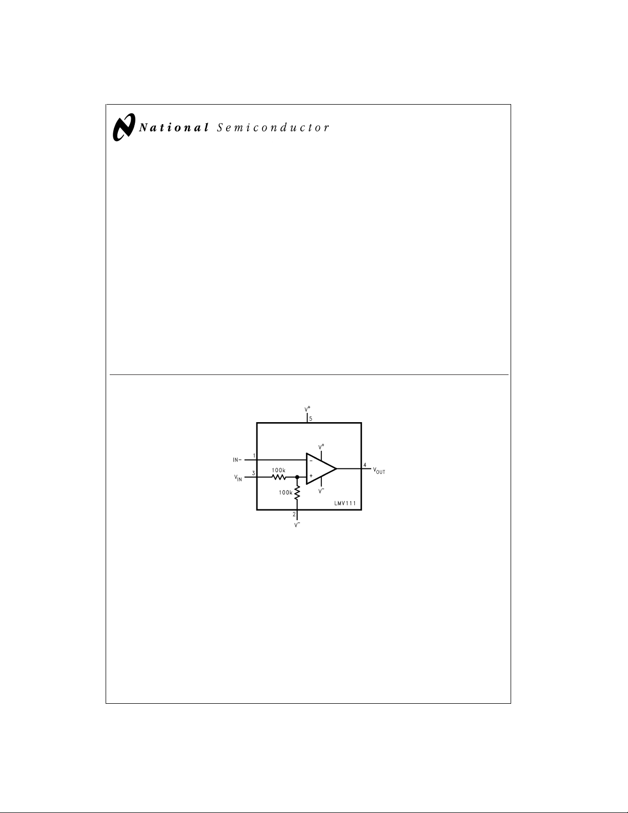
Connection Diagrams
Features
(For 5V Supply, Typical Unless Otherwise Noted)
n Resistor ratio matching 1%(typ)
n Space saving package SC70-5 & SOT23-5
n Industrial temp. range −40˚C to +85˚C
n Low supply current 130µA
n Gain-bandwidth product 1MHz
n Rail-to-Rail output swing
n Guaranteed 2.7V and 5V performance
Applications
n General purpose portable devices
n Active filters
n Mobile communications
n Battery powered electronics
n Microphone preamplifiers
DS101262-21
© 1999 National Semiconductor Corporation DS101262 www.national.com
Page 2
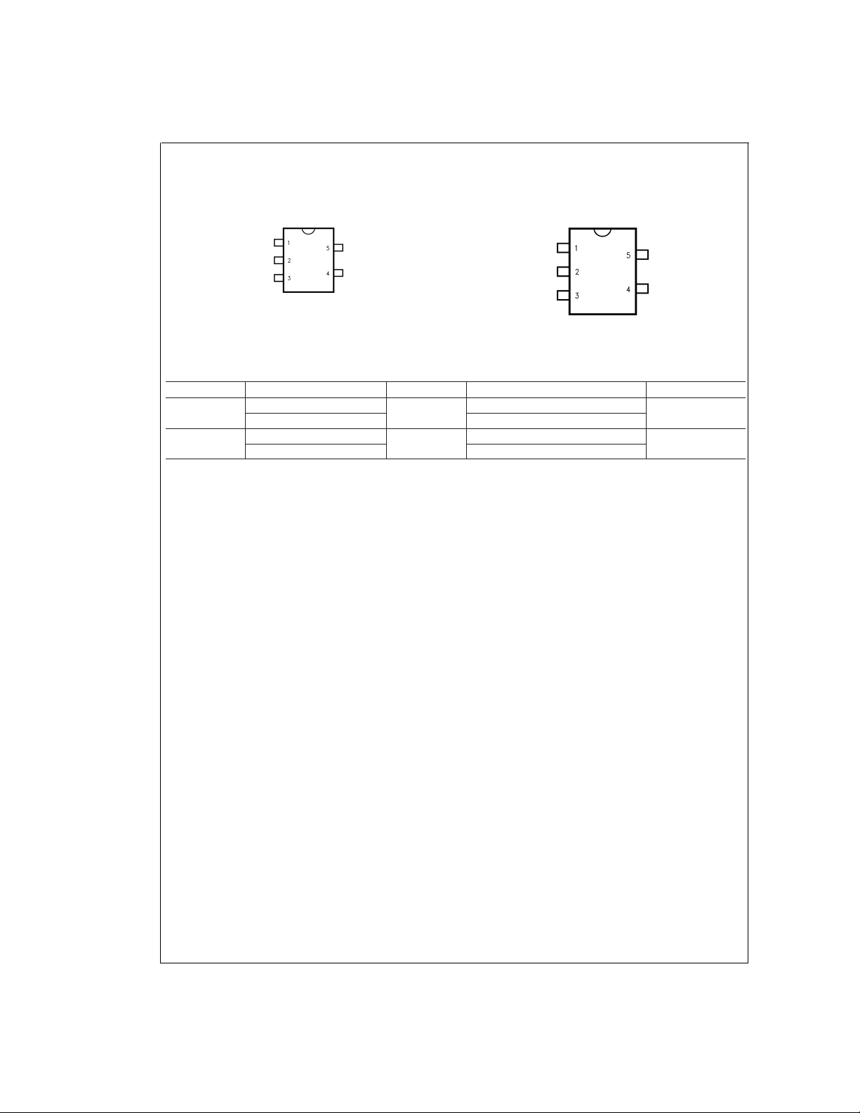
Connection Diagrams (Continued)
LMV111
5-Pin SC70-5
(M7)
DS101262-19
Top View
5-Pin SOT23-5
(M5)
DS101262-20
Top View
Ordering Information
Package Part Number Marking Transport Media NSC Drawing
SC70-5
SOT23-5
LMV111M7
LMV111M7X 3k Units Tape and Reel
LMV111M5
LMV111M5X 3k Units Tape and Reel
A42
A37A
1k Units Tape and Reel
1k Units Tape and Reel
MAA05A
MA05B
www.national.com 2
Page 3
Absolute Maximum Ratings (Note 1)
If Military/Aerospace specified devices are required,
please contact the National Semiconductor Sales Office/
Distributors for availability and specifications.
ESD Tolerance (Note 2)
Machine Model 200V
Human Body Model 1500V
Supply Voltage (V
Output Short Circuit to V
Output Short Circuit to V
Storage Temp. Range −65˚C to 150˚C
+–V−
) 5.5V
+
−
(Note 3)
(Note 4)
Junction Temp. (T
max) (Note 5) 150˚C
J
Mounting Temperature
Infrared or Convection (20 sec) 235˚C
Operating Ratings (Note 1)
Supply Voltage 2.7V to 5.0V
Temperature Range −40˚C ≤ T
Thermal Resistance (θ
)
JA
5-pin SC70-5 478˚C/W
5-pin SOT23-5 265˚C/W
≤ 85˚C
J
LMV111
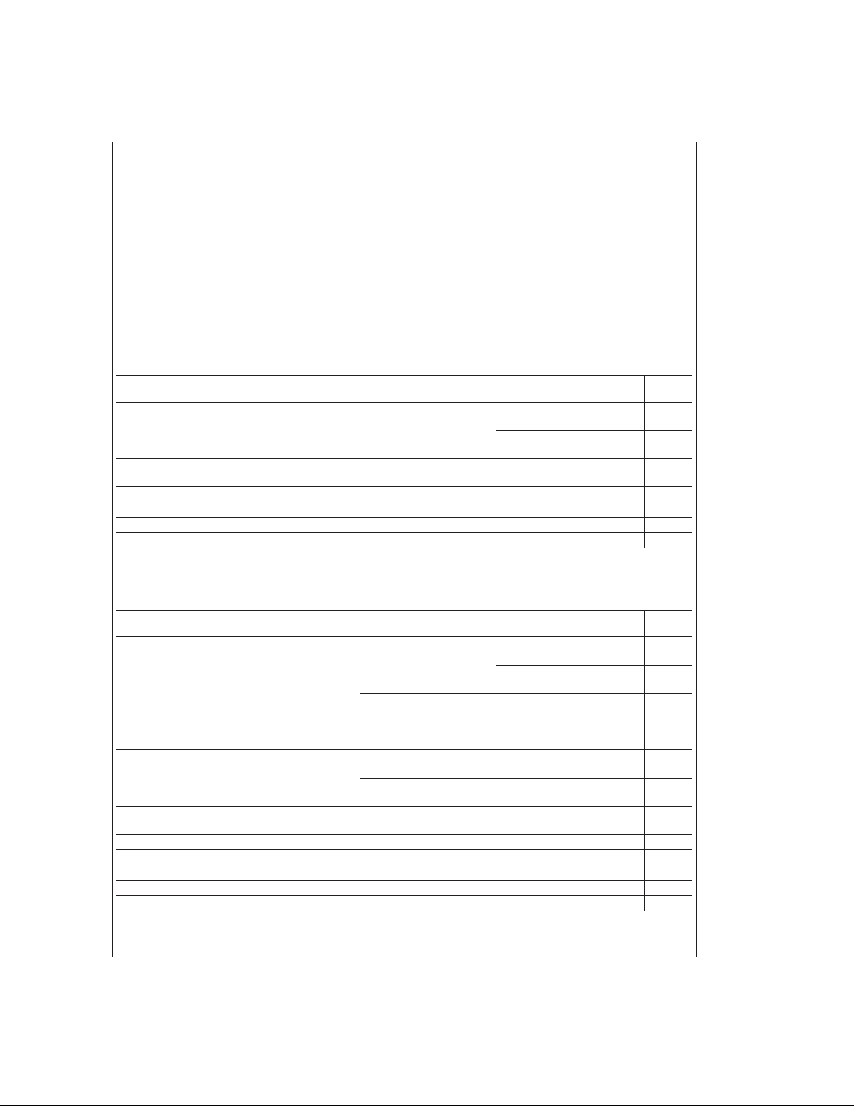
2.7V Electrical Characteristics
Unless otherwise specified, all limits guaranteed for TJ= 25˚C, V+= 2.7V, V−= 0V, VO=V+/2 and R
its apply at the temperature extremes.
Symbol Parameter Conditions
V
O
Output Swing R
=
10kΩ to 1.35V V
L
Typ
(Note 6)
+
−0.01 V+−0.1 V
0.06 0.18 V
I
S
Supply Current 80 170 µA
Resistor Ratio Matching 1
GBWP Gain-Bandwidth Product C
Φ
m
G
m
Phase Margin 60 Deg
Gain Margin 10 dB
=
200pF 1 MHz
L
>
1MΩ.Boldface lim-
L
Limit
(Note 7)
Units
min
max
max
%
5V Electrical Characteristics
Unless otherwise specified, all limits guaranteed for TJ= 25˚C, V+= 5V, V−= 0V, VO=V+/2 and R
apply at the temperature extremes.
Symbol Parameter Conditions
V
O
Output Swing RL=2kΩto 2.5V V+−0.04 V+−0.3
Typ
(Note 6)
0.12 0.3
R
= 10kΩ to 2.5V V+−0.01 V+−0.1
L
0.065 0.18
I
O
Output Current Sourcing, V
Sinking, V
I
S
Supply Current 130 250
=
OV 60 5 mA
O
=
5V 160 10 mA
O
Resistor Ratio Matching 1
GBWP Gain-Bandwidth Product C
=
200pF 1 MHz
L
φm Phase Margin 60 Deg
G
m
Gain Margin 10 dB
SR Slew Rate (Note 8) 1 V/µs
Note 1: Absolute Maximum Ratings indicate limits beyond which damage to the device may occur. Operating Ratings indicate conditions for which the device is intended to be functional, but specific performance is not guaranteed. For guaranteed specifications and the test conditions, see the Electrical Characteristics.
Note 2: Human body model, 1.5kΩ in series with 100pF. Machine model, 0Ω in series with 100pF.
>
1MΩ.Boldface limits
L
Limit
(Note 7)
+
−0.4
V
0.4
+
−0.2
V
0.28
350
Units
V
min
V
max
V
min
V
max
min
min
µA
max
%
www.national.com3
Page 4

5V Electrical Characteristics (Continued)
Note 3: Shorting circuit output to V+will adversely affect reliability.
LMV111
Note 4: Shorting circuit output to V
Note 5: The maximum power dissipation is a function of T
=(T
P
D
Note 6: Typical values represent the most likely parametric norm.
Note 7: All limits are guaranteed by testing or statistical analysis.
Note 8: Connected as voltage follower with 3V step input. Number specified is the slower of the positive and negative slew rates.
)/θJA. All numbers apply for packages soldered directly into a PC board.
J(max)–TA
-
will adversely affect reliability.
, θJA, and TA. The maximum allowable power dissipation at any ambient temperature is
J(max)
Typical Performance Characteristics (Unless otherwise specified, V
25˚C.)
Supply Current vs.
Supply Voltage
DS101262-1
Sinking Current vs.
Output Voltage
Sourcing Current vs.
Output Voltage
Sinking Current vs.
Output Voltage
Sourcing Current vs.
Output Voltage
DS101262-2
Open Loop Frequency vs.
Response
= +5V, single supply, TA=
S
DS101262-3
DS101262-4
Open Loop Frequency vs.
Response
DS101262-7
www.national.com 4
Open Loop Frequency
Response vs. Temperature
DS101262-5
DS101262-8
DS101262-6
Gain and Phase vs.
Capacitive Load
DS101262-9
Page 5

Typical Performance Characteristics (Unless otherwise specified, V
25˚C.) (Continued)
= +5V, single supply, TA=
S
LMV111
Gain and Phase vs.
Capacitive Load
DS101262-10
Non-Inverting Small Signal Pulse
Response
DS101262-13
Open Loop Output
Impedance vs. Frequency
Slew Rate vs.
Supply Voltage
DS101262-11
Inverting Large Signal Pulse
Response
DS101262-14
Short Circuit Current vs.
Temperature (Sinking)
Non-Inverting Large Signal Pulse
Response
DS101262-12
Inverting Small Signal Pulse
Response
DS101262-15
Short Circuit Current vs.
Temperature (Sourcing)
DS101262-16
DS101262-17
DS101262-18
www.national.com5
Page 6

Typical Performance Characteristics (Unless otherwise specified, V
25˚C.) (Continued)
LMV111
Output Voltage Swing vs.
Supply Voltage
DS101262-22
Application Section
The LMV111 integrates a rail-to-rail op amp and a V+/2 bias
circuit into one ultra tiny package. With its small footprint and
reduced component count for bias network, it enables the
design of smaller portable electronic products, such as cellular phones, pagers, PDAs, PCMCIA cards, etc. In addition,
the integration solution minimizes printed circuit board stray
capacitance, and reduces the complexity of circuit design.
The core op amp of this family is National’s LMV321.
1.0 Supply Bypassing
The application circuits in this datasheet do not show the
power supply connections and the associated bypass capacitors for simplification. When the circuits are built, it is always required to have bypass capacitors. Ceramic disc capacitors (0.1µF) or solid tantalum (1µF) with short leads, and
located close to the IC are usually necessary to prevent interstage coupling through the power supply internal impedance. Inadequate bypassing will manifest itself by a low frequency oscillation or by high frequency instabilities.
Sometimes, a 10µF (or larger) capacitor is used to absorb
low frequency variations and a smaller 0.1µF disc is paralleled across it to prevent any high frequency feedback
through the power supply lines.
2.0 Input Voltage Range
The input voltage should be within the supply rails. The ESD
protection circuitry at the input of the device includes a diode
between the input pin and the negative supply pin. Driving
the input more than 0.6V (at 25˚C) beyond the negative supply will turn on the diode and cause signal distortions.
3.0 Capacitive Load Tolerance
The LMV111 can directly drive 200pF capacitive load with
unity gain without oscillation. The unity-gain follower is the
most sensitive configuration to capacitive loading. Direct capacitive loading reduces the phase margin of amplifiers. The
combination of the amplifier’s output impedance and the capacitive load induces phase lag. This results in either an underdamped pulse or oscillation. To drive a heavier capacitive
load, a resistive isolation can be used as shown in
Figure 1
.
FIGURE 1. Resistive Isolation of a Heavy Capacitive
The isolation resistor R
stability by adding more phase margin to the overall system.
The desired performance depends on the value of R
50Ω to 100Ω isolation resistor is recommended for initial
evaluation. The bigger the R
stable V
OUT
will be.
= +5V, single supply, TA=
S
DS101262-23
Load
and the CLform a pole to increase
iso
resistor value, the more
iso
.A
iso
www.national.com 6
Page 7

Application Section (Continued)
4.0 Phase Inverting AC Amplifier
A single supply phase invertingAC amplifier is shown in
ure 2
. The output voltage is biased at mid-supply, and AC input signal is amplified by (R
inputAC coupling capacitor to block DC potentials.A capaci-
). Capacitor CINacts as an
2/R1
tor of 0.1µF or larger can be used. The output of the LMV111
can swing rail-to-rail. To avoid output distortion, the
peak-to-peak amplitude of the input AC signal should be less
than V
CC(R1/R2
).
It is recommended that a small-valued capacitor is used
across the feedback resistor R
lems, prevent peaking of the response, and limit the band-
to eliminate stability prob-
2
width of the circuit. This can also help to reduce high frequency noise and some other interference.
Fig-
LMV111
DS101262-25
FIGURE 3. Fixed Current Source
6.0 Difference Amplifier
The difference amplifier allows the subtraction of two voltages or, as a special case, the cancellation of a signal common to two inputs. It is useful as a computational amplifier, in
making a differential to single-ended conversion or in rejecting a common mode signal.
DS101262-24
FIGURE 2. Phase Inverting AC Amplifier
5.0 Fixed Current Source
Figure 3
A multiple fixed current source is show in
ence voltage (V
by the voltage divider (R3and R4). Negative feedback is
= 2.5V) is established across resistor R
REF
used to cause the voltage drop across R
V
. This controls the emitter current of transistor Q1 and if
REF
we neglect the base current of Q1 and Q2, essentially this
. A refer-
to be equal to
1
same current is available out of the collector of Q1. A Darlington connection can be used to reduce errors due to the
bias current of Q1.
3
DS101262-26
FIGURE 4. Difference Amplifier
www.national.com7
Page 8

Physical Dimensions inches (millimeters) unless otherwise noted
LMV111
5-Pin SC70-5 Tape and Reel
Order Numbers LMV111M7 and LMV111M7X
NS Package Number MAA05A
www.national.com 8
Page 9

Physical Dimensions inches (millimeters) unless otherwise noted (Continued)
LMV111 Operational Amplifier with Bias Network
5-Pin SOT23-5 Tape and Reel
Order Numbers LMV111M5 and LMV111M5X
NS Package Number MA05B
LIFE SUPPORT POLICY
NATIONAL’S PRODUCTS ARE NOT AUTHORIZED FOR USE AS CRITICAL COMPONENTS IN LIFE SUPPORT
DEVICES OR SYSTEMS WITHOUT THE EXPRESS WRITTEN APPROVAL OF THE PRESIDENT AND GENERAL
COUNSEL OF NATIONAL SEMICONDUCTOR CORPORATION. As used herein:
1. Life support devices or systems are devices or
systems which, (a) are intended for surgical implant
into the body, or (b) support or sustain life, and
whose failure to perform when properly used in
accordance with instructions for use provided in the
2. A critical component is any component of a life
support device or system whose failure to perform
can be reasonably expected to cause the failure of
the life support device or system, or to affect its
safety or effectiveness.
labeling, can be reasonably expected to result in a
significant injury to the user.
National Semiconductor
Corporation
Americas
Tel: 1-800-272-9959
Fax: 1-800-737-7018
Email: support@nsc.com
www.national.com
National does not assume any responsibility for use of any circuitry described, no circuit patent licenses are implied and National reserves the right at any time without notice to change said circuitry and specifications.
National Semiconductor
Europe
Fax: +49 (0) 1 80-530 85 86
Email: europe.support@nsc.com
Deutsch Tel: +49 (0) 1 80-530 85 85
English Tel: +49 (0) 1 80-532 78 32
Français Tel: +49 (0) 1 80-532 93 58
Italiano Tel: +49 (0) 1 80-534 16 80
National Semiconductor
Asia Pacific Customer
Response Group
Tel: 65-2544466
Fax: 65-2504466
Email: sea.support@nsc.com
National Semiconductor
Japan Ltd.
Tel: 81-3-5639-7560
Fax: 81-3-5639-7507
 Loading...