

Page 1
LMV101/102/105/110
Fixed-Gain Amplifiers
LMV101/102/105/110 Fixed-Gain Amplifiers
December 1999
General Description
The LMV101/102/105/110 fixed-gain amplifier family integrates a rail-to-rail op amp, two internal gain-setting resistors
+
andaV
/2 bias circuit into one ultra tiny package, SC70-5 or
SOT23-5. Fixed inverting gains of −1, −2, −5, and −10 are
available.
The core op amp in this series is an LMV321, which provides
rail-to-rail output swing, excellent speed-power ratio, 1MHz
bandwidth, and 1V/µs of slew rate with low supply current.
The LMV101/102/105/110 family reduces external component count. It is the most cost effective solution for applications where low voltage operation, low power consumption,
space savings, and reliable performance are needed. It enables the design of small portable electronic devices, and allows the designer to place the device closer to the signal
source to reduce noise pickup and increase signal integrity.
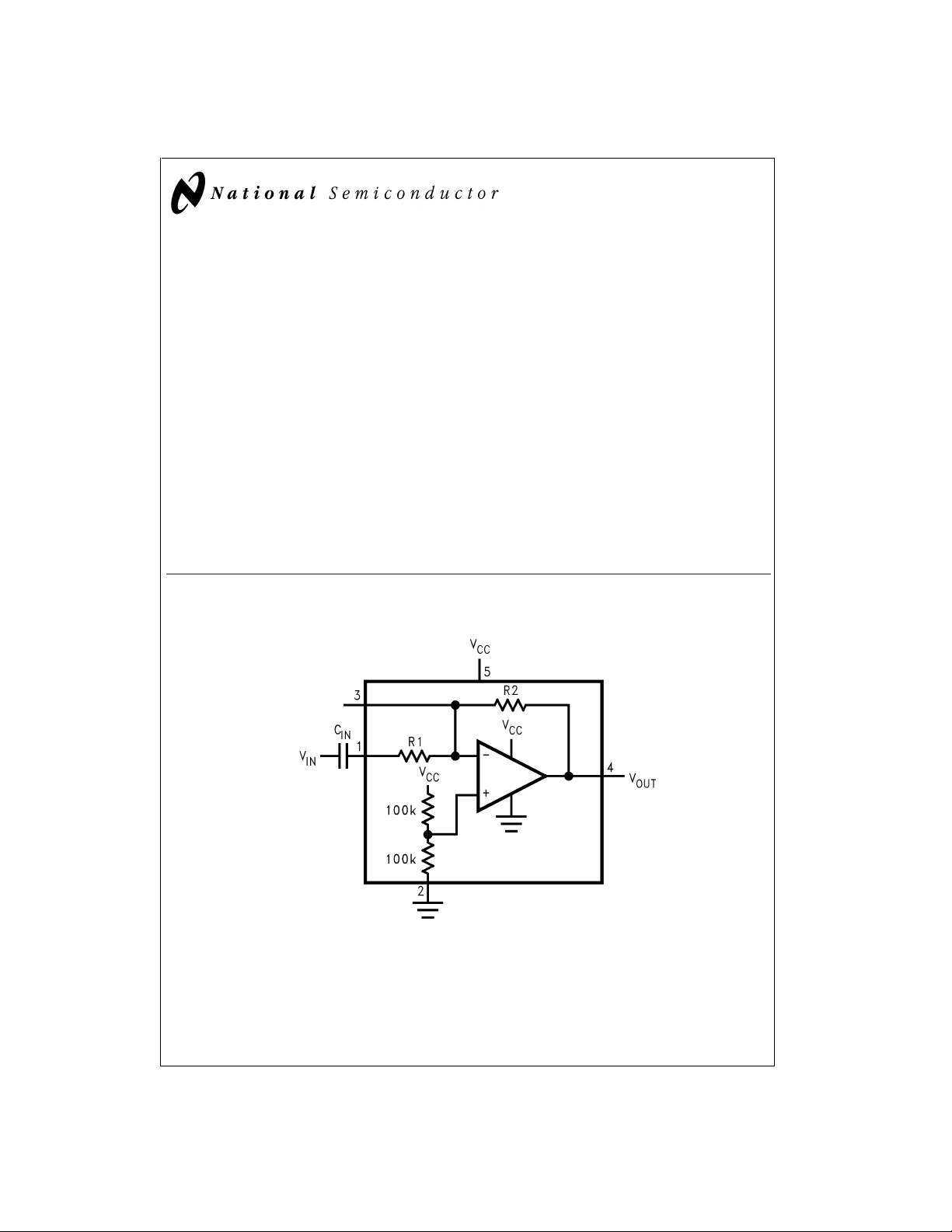
Typical Application
Phase Inverting AC Amplifier
Features
(For 5V Supply, Typical Unless Otherwise Noted)
n Fixed inverting gain available −1,−2,−5,−10
n DC gain accuracy
— LMV101/102/105 2%(typ)
— LMV110 6%(typ)
n Space saving packages SC70-5 & SOT23-5
n Industrial temperature range −40˚C to +85˚C
n Low supply current 130µA
n Rail-to-Rail output swing
n Guaranteed 2.7V and 5V performance
@
2.7V supply
Applications
n General purpose portable devices
n Mobile communications
n Battery powered electronics
n Active filters
n Microphone preamplifiers
DS101234-10
=
V
0.5V
OUT
© 1999 National Semiconductor Corporation DS101234 www.national.com
CC−VIN(R2/R1
)
Page 2
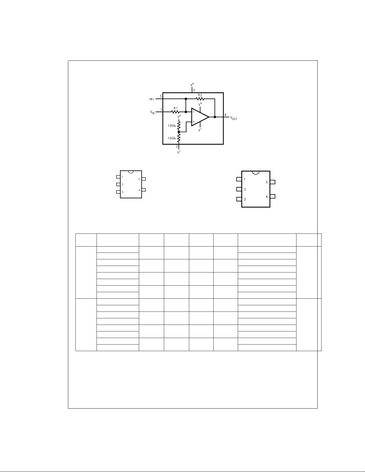
Connection Diagrams
LMV101/102/105/110
5-Pin SC70-5 (M7)
Ordering Information
Package
SC70-5
SOT23-5
Part number Marking DC Gain R1 R2 Transport Media
LMV101M7
LMV101M7X 3k Units Tape and Reel
LMV102M7
LMV102M7X 3k Units Tape and Reel
LMV105M7
LMV105M7X 3k Units Tape and Reel
LMV110M7
LMV110M7X 3k Units Tape and Reel
LMV101M5
LMV101M5X 3k Units Tape and Reel
LMV102M5
LMV102M5X 3k Units Tape and Reel
LMV105M5
LMV105M5X 3k Units Tape and Reel
LMV110M5
LMV110M5X 3k Units Tape and Reel
DS101234-1
A38 −1 100k 100k
A39 −2 100k 200k
A40 −5 50k 250k
A41 −10 10k 100k
A33A −1 100k 100k
A34A −2 100k 200k
A35A −5 50k 250k
A36A −10 10k 100k
DS101234-2
5-Pin SOT23-5 (M5)
DS101234-3
1k Units Tape and Reel
1k Units Tape and Reel
1k Units Tape and Reel
1k Units Tape and Reel
1k Units Tape and Reel
1k Units Tape and Reel
1k Units Tape and Reel
1k Units Tape and Reel
NSC
Drawing
MAA05A
MA05B
www.national.com 2
Page 3
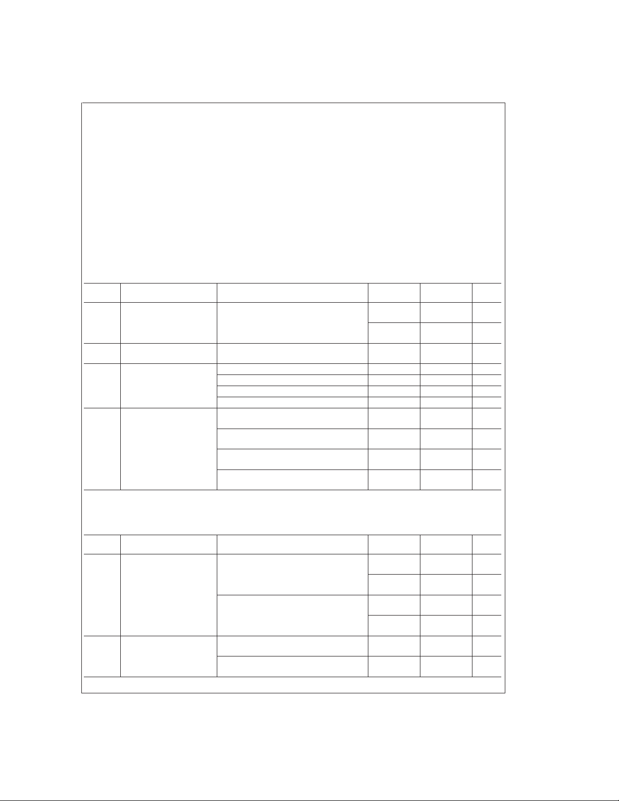
Absolute Maximum Ratings (Note 1)
If Military/Aerospace specified devices are required,
please contact the National Semiconductor Sales Office/
Distributors for availability and specifications.
ESD Tolerance (Note 2)
Machine Model 200V
Human Body Model 1500V
Supply Voltage (V
Output Short Circuit to V
Output Short Circuit to V
Mounting Temperature
Infrared or Convection (20 sec) 235˚C
+-V−
) 5.5V
+
−
(Note 3)
(Note 4)
Storage Temperature Range -65˚C to 150˚C
Junction Temperature (T
(Note 5)
, max)
J
150˚C
Operating Ratings (Note 1)
Supply Voltage 2.7V to 5.0V
Temperature Range −40˚C ≤ T
Thermal resistance (θ
)
JA
5-pin SC70-5 478˚C/W
5-pin SOT23-5 265˚C/W
≤ 85˚C
J
LMV101/102/105/110
2.7V Electrical Characteristics
Unless otherwise specified, all limits guaranteed for TJ= 25˚C, V
its apply at the temperature extremes.
Symbol Parameter Conditions Typ
V
O
Output Swing RL= 10kΩ to 1.35V V+−0.01 V+−0.1 V
+
=
2.7V, V
−
=
0V, V
+
=
/2 and R
V
O
(Note 6)
0.08 0.18 V
I
S
Supply Current 80 170 µA
DC Gain Accuracy LMV101, Gain=−1 2 5
LMV102, Gain=−2 2 5
LMV105, Gain=−5 2 6
LMV110, Gain=−10 6 12
GBW −3dB Bandwidth LMV101, Gain=−1,
=
R
L
2kΩ,C
=
100pF
L
LMV102, Gain=−2,
=
R
L
2kΩ,C
=
100pF
L
LMV105, Gain=−5,
=
R
L
2kΩ,C
=
100pF
L
LMV110, Gain=−10,
=
R
L
5V Electrical Characteristics
Unless otherwise specified, all limits guaranteed for TJ= 25˚C, V
apply at the temperature extremes.
2kΩ,C
=
100pF
L
+
=
5V, V
−
=
0V, V
O
Symbol Parameter Conditions Typ
V
O
Output Swing RL=2kΩto 2.5V V+−0.04 V+−0.3
1.6 MHz
1.8 MHz
0.8 MHz
0.2 MHz
+
=
/2 and R
V
(Note 6)
0.14 0.3
R
= 10kΩ to 2.5V V+−0.01 V+−0.1
L
0.1 0.18
I
O
Output Current Sourcing, V
Sinking, V
=
0V 60 5 mA
O
=
5V 160 10 mA
O
>
1MΩ. Boldface lim-
L
Max
(Note 7)
>
1MΩ. Boldface limits
L
Max
(Note 7)
+
−0.4
V
0.4
+
−0.2
V
0.28
Units
min
max
max
%
%
%
%
Units
V
min
V
max
V
min
V
max
min
min
www.national.com3
Page 4
5V Electrical Characteristics (Continued)
Unless otherwise specified, all limits guaranteed for TJ= 25˚C, V
apply at the temperature extremes.
+
Symbol Parameter Conditions Typ
Supply Current 130 250
DC Gain Accuracy LMV101, Gain=−1 3.5 5
LMV101/102/105/110
I
S
LMV102, Gain=−2 3.5 5
LMV105, Gain=−5 3.5 6
LMV110, Gain=−10 9.0 12
SR Slew Rate (Note 8) 1 V/µs
GBW −3dB Bandwidth LMV101, Gain=−1,
=
R
L
2kΩ,C
=
100pF
L
LMV102, Gain=−2,
=
R
L
2kΩ,C
=
100pF
L
LMV105, Gain=−5,
=
R
L
2kΩ,C
=
100pF
L
LMV110, Gain=−10,
=
R
Note 1: Absolute Maximum Ratings indicate limits beyond which damage tothedevice may occur. Operating Ratings indicate conditions for which the device is intended to be functional, but specific performance is not guaranteed. For guaranteed specifications and the test conditions, see the Electrical Characteristics.
Note 2: Human body model, 1.5kΩ in series with 100pF. Machine model, 0Ω in series with 100pF.
Note 3: Shorting circuit output to V
Note 4: Shorting circuit output to V
Note 5: The maximum power dissipation is a function of T
=(T
P
D
Note 6: Typical Values represent the most likely parametric norm.
Note 7: All limits are guaranteed by testing or statistical analysis.
Note 8: Number specified is the slower of the positive and negative slew rates.
)/θJA. All numbers apply for packages soldered directly into a PC board.
J(max)–TA
+
will adversely affect reliability.
−
will adversely affect reliability.
L
=
2kΩ,C
J(max)
100pF
L
, θJA, and TA. The maximum allowable power dissipation at any ambient temperature is
=
5V, V
−
=
0V, V
+
=
/2 and R
V
O
(Note 6)
>
1MΩ. Boldface limits
L
Max
(Note 7)
350
1.6 MHz
1.8 MHz
0.8 MHz
0.2 MHz
Units
µA
max
%
%
%
%
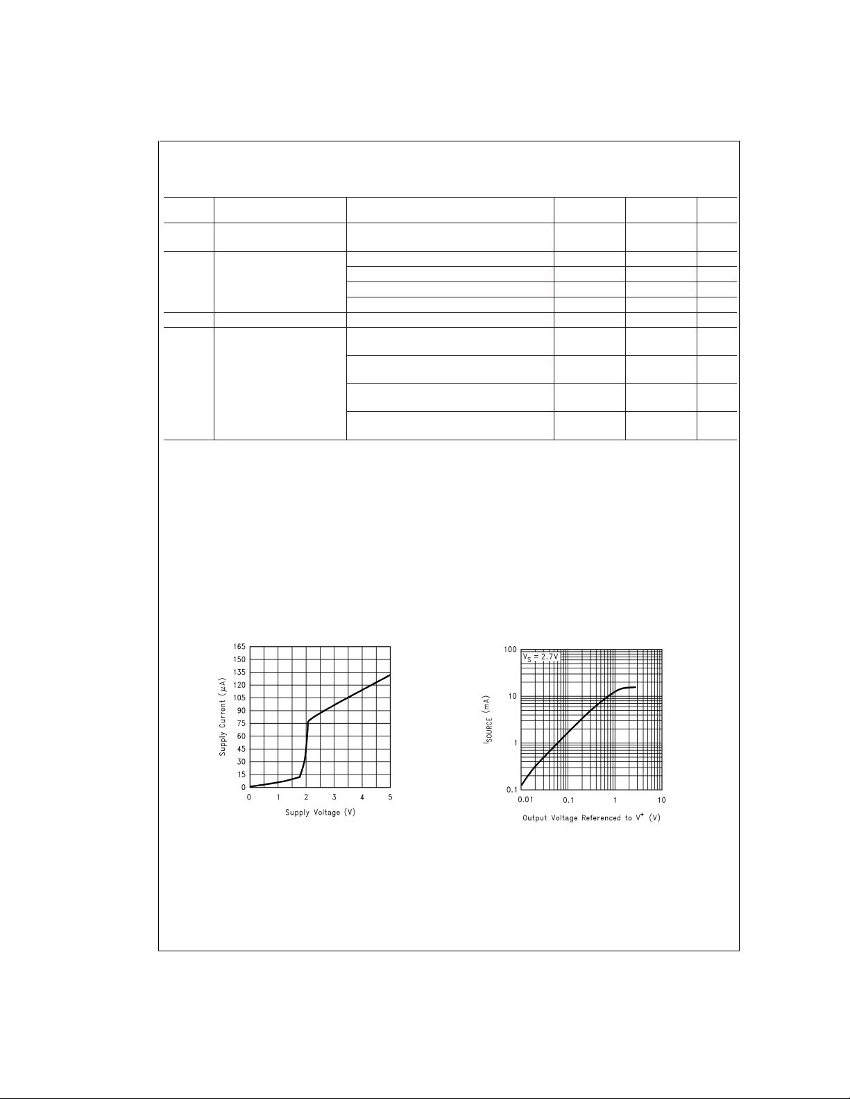
Typical Performance Characteristics (Unless otherwise specified, V
25˚C.)
Supply Current vs.
Supply Voltage
DS101234-22
www.national.com 4
vs. Output Voltage
=
+5V, single supply, T
S
Sourcing Current
DS101234-23
=
A
Page 5

Typical Performance Characteristics (Unless otherwise specified, V
25˚C.) (Continued)
=
+5V, single supply, T
S
LMV101/102/105/110
=
A
Sourcing Current vs.
Output Voltage
Sinking Current vs.
Output Voltage
DS101234-24
Sinking Current vs.
Output Voltage
DS101234-25
Output Voltage Swing vs.
Supply Voltage
LMV101 Close Loop
Frequency Response
DS101234-26
DS101234-27
DS101234-21
LMV101 Close Loop
Frequency Response
DS101234-28
www.national.com5
Page 6

Typical Performance Characteristics (Unless otherwise specified, V
25˚C.) (Continued)
=
+5V, single supply, T
S
=
A
LMV101/102/105/110
LMV102 Close Loop
Frequency Response
LMV105 Close Loop
Frequency Response
DS101234-29
LMV102 Close Loop
Frequency Response
DS101234-30
LMV105 Close Loop
Frequency Response
DS101234-31
LMV110 Close Loop
Frequency Response
DS101234-33
www.national.com 6
DS101234-32
LMV110 Close Loop
Frequency Response
DS101234-34
Page 7

Typical Performance Characteristics (Unless otherwise specified, V
25˚C.) (Continued)
=
+5V, single supply, T
S
LMV101/102/105/110
=
A
Inverting Large Signal Pulse Response
LMV101
DS101234-35
Inverting Large Signal Pulse Response
LMV105
Inverting Large Signal Pulse Response
LMV102
DS101234-37
Inverting Large Signal Pulse Response
LMV110
DS101234-39
Inverting Small Signal Pulse Response
LMV101
DS101234-36
DS101234-41
Inverting Small Signal Pulse Response
LMV102
DS101234-38
www.national.com7
Page 8

Typical Performance Characteristics (Unless otherwise specified, V
25˚C.) (Continued)
=
+5V, single supply, T
S
=
A
LMV101/102/105/110
Inverting Small Signal Pulse Response
LMV105
DS101234-40
Slew Rate vs.
Supply Voltage
Inverting Small Signal Pulse Response
LMV110
DS101234-42
DS101234-43
Application Notes
The LMV101/102/105/110 integrates a rail-to-rail op amp,
two internal gain-setting resistors and a V
one ultra tiny package, SC70-5 or SOT23-5. With its small
footprint and reduced component count for gain stage, it enables the design of smaller portable electronic products,
such as cellular phones, pagers, PDAs, PCMCIA cards, etc.
In addition, the integration solution minimizes printed circuit
board stray capacitance, and reduces the complexity of circuit design.
The core op amp of this family is National’s LMV321.
1.0 Supply Bypassing
The application circuits in this datasheet do not show the
power supply connections and the associated bypass capacitors for simplification. When the circuits are built, it is always required to have bypass capacitors. Ceramic disc capacitors (0.1µF) or solid tantalum (1µF) with short leads, and
located close to the IC are usually necessary to prevent interstage coupling through the power supply internal impedance. Inadequate bypassing will manifest itself by a low frequency oscillation or by high frequency instabilities.
Sometimes, a 10µF (or larger) capacitor is used to absorb
www.national.com 8
+
/2 bias circuit into
low frequency variations and a smaller 0.1µF disc is paralleled across it to prevent any high frequency feedback
through the power supply lines.
2.0 Input Voltage Range
The input voltage should be within the supply rails. The ESD
protection circuitry at the input of the device includes a diode
between the input pin and the negative supply pin. Driving
the input more than 0.6V (at 25˚C) beyond the negative supply will turn on the diode and cause signal distortions. For
applications that require sensing voltages beyond the negative rail, use the LMV111 with external gain setting resistors.
Page 9

Application Notes (Continued)
3.0 Capacitive Load Tolerance
The LMV101/102/105/110 can directly drive 200pF capacitive load with Vs=5V at −1 gain configuration without oscillation. Direct capacitive loading reduces the phase margin of
amplifiers. The combination of the amplifier’s output impedance and the capacitive load induces phase lag. This results
in either an underdamped pulse or oscillation. To drive a
heavier capacitive load, a resistive isolation can be used as
shown in
The isolation resistor R
stability by adding more phase margin to the overall system.
The desired performance depends on the value of R
bigger the R
Figure 2
R
Figure 1
.
DS101234-13
FIGURE 1. Resistive Isolation of a Heavy Capacitive
Load
and the CLform a pole to increase
iso
. The
resistor value, the more stable V
iso
is an output waveform of
and 1000pF for CL.
iso
Figure 1
iso
will be.
OUT
using 100Ω for
larger can be used. The output can swing rail-to-rail. Toavoid
output distortion, the peak-to-peak amplitude of the input AC
signal should be less than V
CC(R1/R2
).
DS101234-10
FIGURE 3. Phase Inverting AC Amplifier
It is recommended that a small-valued capacitor be used
across the feedback resistor (R
lems, prevent peaking of the response, and limit the band-
) to eliminate stability prob-
2
width of the circuit. This can also help to reduce high frequency noise and some other interference. (See
Figure 4
LMV101/102/105/110
)
FIGURE 2. Pulse Response of LMV101 in
Figure 1
4.0 Phase Inverting AC Amplifier
A single supply phase inverting AC amplifier can be easily
Figure 3
built with the LMV101/102/105/110 series (
). The
output voltage is biased at mid-supply, and AC input signal is
amplified by (R
pling capacitor to block DC potentials. A capacitor of 0.1µF or
). Capacitor CINacts as an input AC cou-
2/R1
FIGURE 4.
5.0 Microphone preamplifier
Most microphones have a low output voltage level. This output signal needs to be amplified so that it can feed the next
stage with optimal level.
Figure 5
shows a microphone
preamplifier circuit with the LMV110. This microphone
preamplifier can provide 20dB gain. It can be implemented in
PCs, PDAs, and mobile phones.
Input capacitor C
blocks any DC voltage from the previous stage to prevent
serves two important functions. First, it
IN
the output from shifting to some unwanted DC level. This
could cause the output to saturate when audio signal is ap-
DS101234-12
plied at the input. Second, the C
form a low pass filter to block any low frequency noise. The
and the 10k input resistor
IN
cut-off frequency of this low pass filter is given by,
where R
to block the DC output from the next stage. R
=
10kΩ in LMV110. Output capacitor C
1
according to the microphone requirement.
DS101234-11
OUT
is selected
bias
www.national.com9
is used
Page 10

Application Notes (Continued)
LMV101/102/105/110
FIGURE 5. Microphone Preamplifier with 20dB Gain
To improve power supply ripple rejection of the above microphone preamplifier, another capacitor and a pot can be connected to pin 1 as shown in
two capacitors at audio frequencies are low. The R
be adjusted so that the supply ripples injected through both
the inverting input and the non-inverting input cancel each
other at the output. If we ignore the impedance of the capacitors, we can select the pot value based on the following
equation:
Z
is the output impedance of the microphone, and G is
OUT
the gain of the preamplifier in absolute value.
Figure 6
. The impedance of the
DS101234-15
POT
can
6.0 Adjustable-Gain Amplifier
The LMV101/102/105/110not only provides fixed gain of −1,
−2, −5, and −10, it can also be configured for different gains
by adding only one external resistor.
Youcan decrease the gain by putting a resistor in series with
pin1(
Figure 7
resistor from pin 1 to pin 3 (
). You can increase the gain by connecting a
Figure 8
).
DS101234-18
FIGURE 7. Decreased Gain
DS101234-17
FIGURE 6. Improved Ripple Rejection
www.national.com 10
DS101234-19
FIGURE 8. Increased Gain
If you are using the LMV110 as a microphone preamplifier
Figure 5
for an electret microphone (
), and the output impedance of the microphone is 1kΩ, then the gain of the preamplifier is
If we choose a small value for R, then we could get a preamplifier with a gain close to 100 (40dB), which is 10 times the
gain provided by LMV110.
Page 11

Physical Dimensions inches (millimeters) unless otherwise noted
LMV101/102/105/110
Order Numbers LMV101M7, LMV101M7X, LMV102M7, LMV102M7X,
5-Pin SC70-5 Tape and Reel
LMV105M7, LMV105M7X, LMV110M7 or LMV110M7X
NS Package Number MAA05A
www.national.com11
Page 12

Physical Dimensions inches (millimeters) unless otherwise noted
LMV101/102/105/110 Fixed-Gain Amplifiers
Order Numbers LMV101M5, LMV101M5X, LMV102M5, LMV102M5X,
5-Pin SOT23-5 Tape and Reel
LMV105M5, LMV105M5X, LMV110M5 or LMV110M5X
NS Package Number MA05B
LIFE SUPPORT POLICY
NATIONAL’S PRODUCTS ARE NOT AUTHORIZED FOR USE AS CRITICAL COMPONENTS IN LIFE SUPPORT
DEVICES OR SYSTEMS WITHOUT THE EXPRESS WRITTEN APPROVAL OF THE PRESIDENT AND GENERAL
COUNSEL OF NATIONAL SEMICONDUCTOR CORPORATION. As used herein:
1. Life support devices or systems are devices or
systems which, (a) are intended for surgical implant
into the body, or (b) support or sustain life, and
whose failure to perform when properly used in
accordance with instructions for use provided in the
2. A critical component is any component of a life
support device or system whose failure to perform
can be reasonably expected to cause the failure of
the life support device or system, or to affect its
safety or effectiveness.
labeling, can be reasonably expected to result in a
significant injury to the user.
National Semiconductor
Corporation
Americas
Tel: 1-800-272-9959
Fax: 1-800-737-7018
Email: support@nsc.com
www.national.com
National does not assume any responsibility for use of any circuitry described, no circuit patent licenses are implied and National reserves the right at any time without notice to change said circuitry and specifications.
National Semiconductor
Europe
Fax: +49 (0) 1 80-530 85 86
Email: europe.support@nsc.com
Deutsch Tel: +49 (0) 1 80-530 85 85
English Tel: +49 (0) 1 80-532 78 32
Français Tel: +49 (0) 1 80-532 93 58
Italiano Tel: +49 (0) 1 80-534 16 80
National Semiconductor
Asia Pacific Customer
Response Group
Tel: 65-2544466
Fax: 65-2504466
Email: sea.support@nsc.com
National Semiconductor
Japan Ltd.
Tel: 81-3-5639-7560
Fax: 81-3-5639-7507
 Loading...