

Page 1
March 28, 2008
LMV1088
Dual Input, Far Field Noise Suppression Microphone
Amplifier with Automatic Calibration Ability
General Description
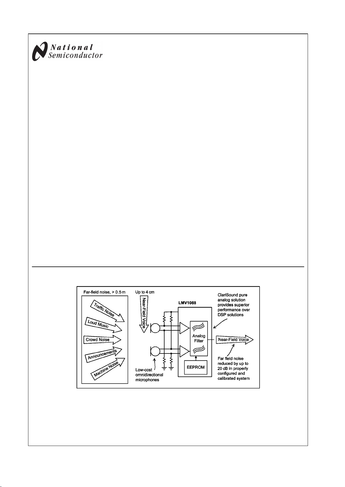
The LMV1088 amplifies near-field voice signals within 4cm of
the microphones while rejecting far-field acoustic noise
greater than 0.5m from the microphones. Up to 20dB of farfield rejection is possible in a properly configured and calibrated system.
Part of the Powerwise® family of energy efficient solutions,
the LMV1088 consumes 1mA of supply current while providing superior performance to DSP solutions consuming over
10 times the power.
A fast calibration during the manufacturing test process allows the LMV1088 to compensate the entire microphone
system. This calibration includes mismatch in microphone
gain and frequency response, as well as acoustical path variances. The LMV1088 stores the calibration coefficients in onboard EEPROM. The calibration is initiated by I2C command
or by pin control.
The dual microphone inputs are differential to provide excellent noise immunity. The microphones are biased with an
internal low-noise bias supply.
Key Specifications
(3.3V supply, unless otherwise specified)
■
Supply voltage 2.7V to 5.5V
■
Supply current 1mA (typ)
■
Signal to noise ratio (A-weighted) 60dB (typ)
■
Total harmonic distortion (A-weighted) 0.1% (typ)
■
Noise cancellation 20dB (typ)
■
PSRR 85dB (typ)
Features
■
Low power consumption
■
No added processing delay
■
Automatic Calibration
■
Space-saving 36 Bump micro SMD package
■
Up to 20dB SNRI
Applications
■
Mobile handsets
■
Mobile and handheld two-way radios
■
Bluetooth and other powered headsets
■
Hand-held voice microphones
■
Portable public address systems
Application of the LMV1088
20213028
PowerWise® is a registered trademark of National Semiconductor Corporation.
© 2008 National Semiconductor Corporation 202130 www.national.com
LMV1088 Dual Input, Far Field Noise Suppression Microphone Amplifier with Automatic
Calibration Ability
Page 2
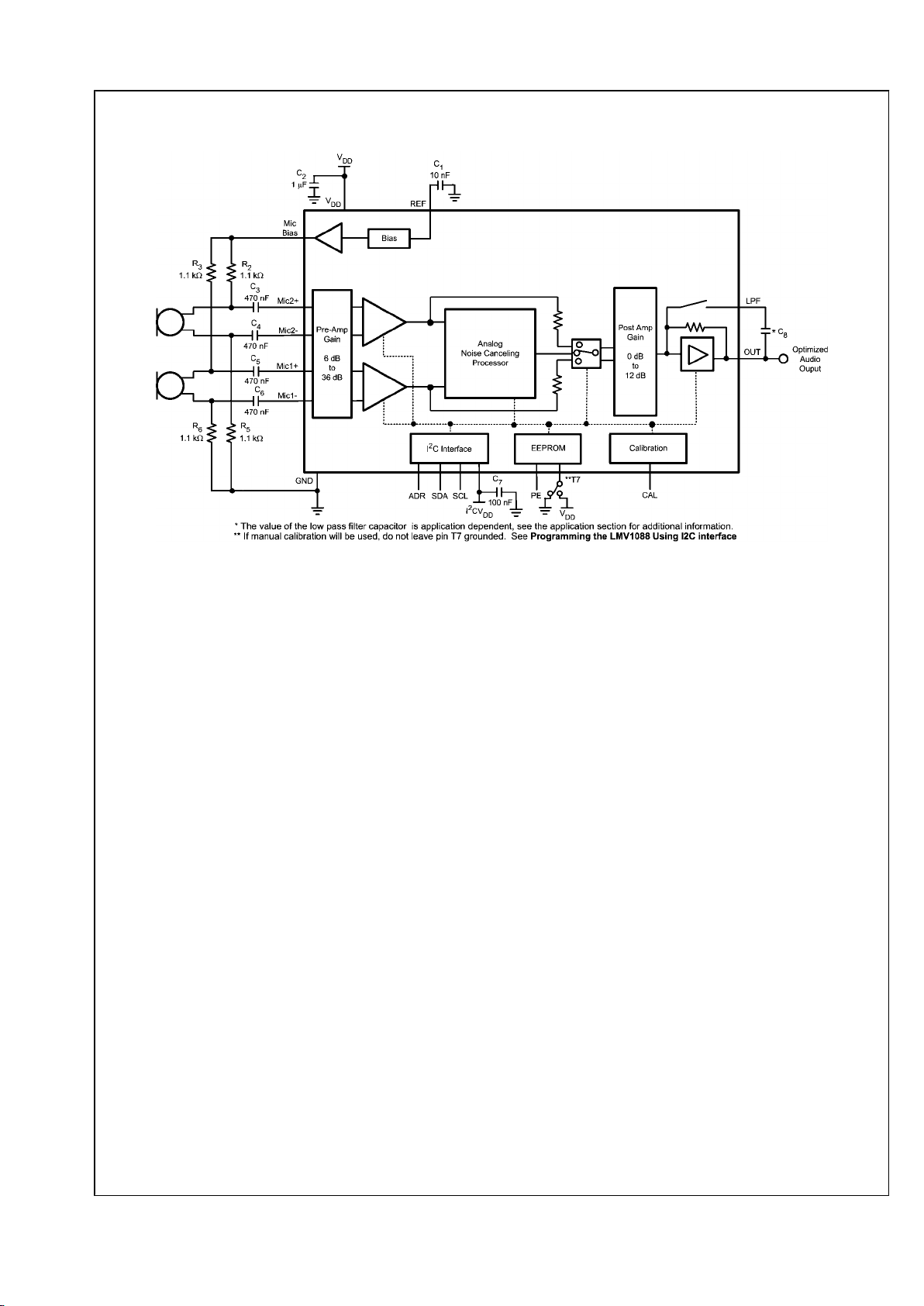
Typical Application
20213041
FIGURE 1. Typical Dual Microphone Far Field noise Cancelling Application
www.national.com 2
LMV1088
Page 3
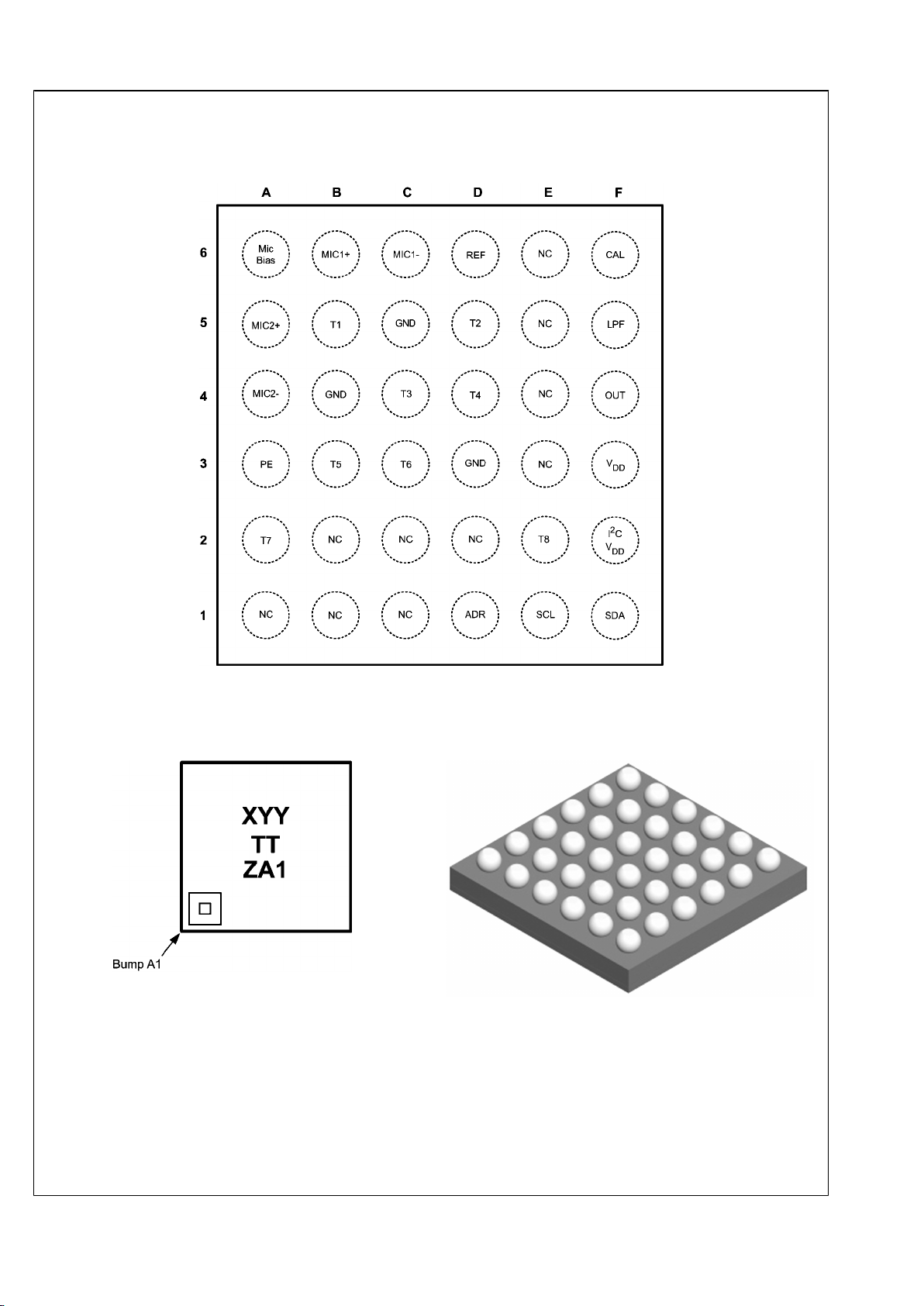
Connection Diagrams
36 Bump micro SMD package
20213030
Top View
Order Number LMV1088RL
See NS Package Number RLA36TTA
36 Bump micro SMD Marking
20213031
Top View
X = Plant Code
YY = Date Code
TT= Die Tracability
ZA1 = LMV1088RL
micro SMD Package View
20213033
Bottom View
3 www.national.com
LMV1088
Page 4
TABLE 1. Pin Name and Function
Bump Number Pin Name Pin Function
A1 NC No Connect (Note 1)
A2 T7 Control pin (Note 3)
A3 PE Program Enable EEPROM
A4 MIC2– microphone 2 input —
A5 MIC2+ microphone 2 input +
A6 Mic Bias Bias for Microphones
B1 NC No Connect (Note 1)
B2 NC No Connect (Note 1)
B3 T5 Float(Note 2)
B4 GND Amplifier ground
B5 T1 Float(Note 2)
B6 MIC1+ microphone 1 input +
C1 NC No Connect (Note 1)
C2 NC No Connect (Note 1)
C3 T6 Float(Note 2)
C4 T3 Float(Note 2)
C5 GND Amplifier ground
C6 MIC1– microphone 1 input —
D1 ADR I2C Address select
D2 NC No Connect (Note 1)
D3 GND Amplifier ground
D4 T4 Float(Note 2)
D5 T2 Connect to GND
D6 REF Reference Voltage De-coupling
E1 SCL I2C Clock
E2 T8 Connect to GND
E3 NC No Connect (Note 1)
E4 NC No Connect (Note 1)
E5 NC No Connect (Note 1)
E6 NC No Connect (Note 1)
F1 SDA I2C Data
F2 I2CV
DD
I2C power supply
F3 V
DD
Power Supply
F4 OUT Optimized Audio Out
F5 LPF Lowpasss Filter Capacitor
F6 CAL Calibration Start
Note 1: Connect NC pins to GND for optimum noise performance.
Note 2: Do not ground pins.
Note 3: Force VDD setup for manual calibrations. Force GND setup for calibration circuitry.
www.national.com 4
LMV1088
Page 5
Absolute Maximum Ratings (Note 4)
If Military/Aerospace specified devices are required,
please contact the National Semiconductor Sales Office/
Distributors for availability and specifications.
Supply Voltage 6.0V
Storage Temperature -85°C to +150°C
ESD Rating (Note 7) 2000V
ESD Rating (Note 8) 200V
Junction Temperature (T
JMAX
) 150°C
Mounting Temperature
Infrared or Convection (20 sec.)
235°C
Thermal Resistance
θJA (microSMD)
70°C/W
Soldering Information See AN-112 “microSMD Wafers Level
Chip Scale Package.”
Operating Ratings (Note 5)
Supply Voltage 2.7V to 5.5V
I2CVDD (Note 13) 1.8V to 5.5V
Temperature Range −40°C to 85°C
Electrical Characteristics 3.3V (Note 4)
Unless otherwise specified, all limits guaranteed for TJ = 25°C, VDD = 3.3V, VIN = 18mVPP, pass through mode (Note 11), preamplifier
gain = 20dB, postamplifier gain = -2.5dB, RL = 100kΩ, and CL = 4.7pF.
Symbol Parameter Conditions
LMV1088
Units (Limits)
Typical (Note 9) Limits (Note 10)
SNR
Signal-to-Noise Ratio f = 1kHz, , V
IN
= 18mVPP, A-Weighted 60 dB
VINMax Input Signal f = 1kHz and THD+N < 1% 97 mV
PP
V
out
AC Output Voltage f = 1kHz 500 mV
RMS
DC Output Voltage 800 mV
THD+N
Total Harmonic Distortion + Noise f = 1kHz, VIN = 18mV
PP
0.1 %
Z
IN
Input Impedance 100
kΩ
Z
OUT
Output Impedance 150
Ω
Z
LOAD
R
LOAD
C
LOAD
10
10
kΩ (min)
pF (max)
AMMicrophone Pre Amplifier Gain Range f = 1kHz 6 – 36 dB
A
MR
Microphone Pre Amplifier Gain
Adjustment Resolution
f = 1kHz 2 dB
A
P
Post Amplifier Gain Range
f = 1kHz Pass Through Mode and
Summing Mode
-2.5 – 9.5 dB
f = 1kHz Noise Canceling Mode
(Note 12)
0 – 12 dB
A
PR
Post Amplifier Gain Adjustment
Resolution
f = 1kHz 3 dB
A
CR
Gain Compensation Range
f = 300Hz — f = 3400Hz ±3 dB (max)
A
MD
Gain Matching Difference After
Calibration
f = 300Hz
f = 1kHz
f = 3kHz
0.5
0.5
0.5
dB (max)
dB (max)
dB (max)
T
CAL
Calibration Duration 770 ms (max)
PSRR Power Supply Rejection Ratio
Input Referred, Input AC grounded
f = 217Hz (100mVPP) 85 dB
f = 1kHz (100mVPP) 80 dB
CMRR Common Mode Rejection Ratio f = 1kHz, 60 dB
VBMMicrophone Bias Supply Voltage I
BIAS
= 1mA 2.0 V
ε
VBM
Microphone Bias Supply Noise A-Weighted 10
μV
RMS
I
BM
Total available Microphone Bias
Current
1.2 mA (min)
I
DDQ
Supply Quiescent Current VIN = 0V
1 1.5 mA (max)
I
DDCP
Supply Current during Calibration and
Programming
Calibrating or Programming
EEPROM
28 50 mA (max)
I
DD
Supply Current
Vin = 25mVPP both inputs, Noise
canceling mode
1 1.5 mA (max)
5 www.national.com
LMV1088
Page 6
Digital Interface Characteristics (Notes 4, 13)
Unless otherwise specified, all limits guaranteed for TJ = 25°C, I2CVDD within the Operating Rating (Note 13)
Symbol Parameter Conditions
LMV1088
Units
(Limits)
Typical
(Note 9)
Limits (Note
10)
V
IH
Logic High Input Level SCL, SDA, ADR, CAL, PE pins
0.6xI2CV
DD
V (min)
V
IL
Logic Low Input Level SCL, SDA, ADR, CAL, PE pins
0.4xI2CV
DD
V (max)
ts
CAL
CAL Setup Time 2 ms
th
CAL
CAL Hold time until calibration is
finished
770 ms (min)
ts
PEC
PE Setup Time 2 ms
th
PEC
PE Hold until calibration is finished 770 ms (min)
Note 4: “Absolute Maximum Ratings” indicate limits beyond which damage to the device may occur, including inoperability and degradation of device reliability
and/or performance. Functional operation of the device and/or non-degradation at the Absolute Maximum Ratings or other conditions beyond those indicated in
the Recommended Operating Conditions is not implied. The Recommended Operating Conditions indicate conditions at which the device is functional and the
device should not be operated beyond such conditions. All voltages are measured with respect to the ground pin, unless otherwise specified.
Note 5: The Electrical Characteristics tables list guaranteed specifications under the listed Recommended Operating Conditions except as otherwise modified
or specified by the Electrical Characteristics Conditions and/or Notes. Typical specifications are estimations only and are not guaranteed.
Note 6: The maximum power dissipation must be de-rated at elevated temperatures and is dictated by T
JMAX
, θJC, and the ambient temperature TA. The maximum
allowable power dissipation is P
DMAX
= (T
JMAX
–TA)/ θJA or the number given in the Absolute Maximum Ratings, whichever is lower. For the LMV1088, T
JMAX
=
150°C and the typical θJA for this microSMD package is 70°C/W and for the LLP package θJA is 64°C/W Refer to the Thermal Considerations section for more
information.
Note 7: Human body model, applicable std. JESD22-A114C.
Note 8: Machine model, applicable std. JESD22-A115-A.
Note 9: Typical values represent most likely parametric norms at TA = +25°C, and at the Recommended Operation Conditions at the time of product
characterization and are not guaranteed.
Note 10: Datasheet min/max specification limits are guaranteed by test, or statistical analysis.
Note 11: In Pass Through mode, only one microphone input is active. See also I2C Compatible Interface for more information how to configure the LMV1088.
Note 12: In Noise Canceling Mode there is 2.5dB additional gain before calibration when compared to the other operating modes to compensate for the gain
reduction that is caused by the noise canceling effect.
Note 13: The voltage at I2CVDD must not exceed the voltage on VDD.
www.national.com 6
LMV1088
Page 7
Typical Performance Characteristics Unless otherwise specified, T
J
= 25°C, VDD = 3.3V, VIN =
18mVPP, pass through mode (Note 11), preamplifier gain = 20dB, postamplifier gain = –2.5dB, RL = 100kΩ, and CL = 4.7pF.
Supply Current vs. Supply Voltage
20213021
THD+N vs Frequency, pass through mode Mic1
VIN = 36mV
pp
20213003
THD+N vs Frequency, pass through mode Mic2
VIN = 36mV
pp
20213004
THD+N vs Frequency, Noise canceling mode
signal at Mic1, Mic2 AC shorted, VIN = 36mV
pp
20213005
THD+N vs Frequency, Noise canceling mode
Mic1 AC shorted, signal at Mic2, VIN = 36mV
pp
20213006
THD+N vs Vin, pass through mode Mic1
20213016
7 www.national.com
LMV1088
Page 8
THD+N vs Vin, pass through mode Mic2
20213015
THD+N vs Vin, Noise canceling mode
signal at Mic1, Mic2 AC shorted
20213014
THD+N vs Vin, Noise canceling mode
Mic1 AC shorted, signal at Mic2
20213017
PSRR vs Frequency, pass through mode Mic1,
Mic1+ Mic2 AC shorted
20213018
PSRR vs Frequency, pass through mode Mic2,
Mic1+ Mic2 AC shorted
20213019
PSRR vs Frequency, Noise canceling mode ,
Mic1+ Mic2 AC shorted
20213020
www.national.com 8
LMV1088
Page 9

PSRR vs Frequency, Microphone Bias ,
Mic1+ Mic2 AC shorted
20213022
9 www.national.com
LMV1088
Page 10

Application Data
I2C Compatible Interface
I2C SIGNALS
The LMV1088 pin SCL is used for the I2C clock SCL and the
pin SDA is used for the I2C data signal SDA. Both these sig-
nals need a pull-up resistor according to I2C specification. The
LMV1088 can be controlled on two slave addresses depending on the logical level at the I2C address pin. The two I2C
slave address for LMV1088 are given inTable 2 .
TABLE 2. Chip Address
D7 D6 D5 D4 D3 D2 D1 D0
1st Chip Address
I2C Adress='0'
1 1 0 0 1 1 0 W/R
2nd Chip Address
I2C Adress='1'
1 1 0 0 1 1 1 W/R
I2C DATA VALIDITY
The data on SDA line must be stable during the HIGH period
of the clock signal (SCL). In other words, state of the data line
can only be changed when SCL is LOW.
202130q1
I2C Signals: Data Validity
I2C START AND STOP CONDITIONS
START and STOP bits classify the beginning and the end of
the I2C session. START condition is defined as SDA signal
transitioning from HIGH to LOW while SCL line is HIGH.
STOP condition is defined as the SDA transitioning from LOW
to HIGH while SCL is HIGH. The I2C master always generates
START and STOP bits. The I2C bus is considered to be busy
after START condition and free after STOP condition. During
data transmission, I2C master can generate repeated START
conditions. First START and repeated START conditions are
equivalent, function-wise.(Note 14)
202130q2
I2C Start Stop Conditions
Note 14: The master should issue STOP after no acknowledgement.
TRANSFERRING DATA
Every byte put on the SDA line must be eight bits long, with
the most significant bit (MSB) being transferred first. Each
byte of data has to be followed by an acknowledge bit. The
acknowledge related clock pulse is generated by the master.
The transmitter releases the SDA line (HIGH) during the acknowledge clock pulse. The receiver must pull down the SDA
line during the 9th clock pulse, signifying an acknowledge. A
receiver which has been addressed must generate an acknowledge after each byte has been received.
After the START condition, the I2C master sends a chip address. This address is seven bits long followed by an eighth
bit which is a data direction bit (R/W). The LMV1088 address
is 110011002or 110011102. For the eighth bit, a “0” indicates
a WRITE and a “1” indicates a READ. The second byte selects the register to which the data will be written. The third
byte contains data to write to the selected register.
202130q3
I2C Chip Address
Register changes take effect at the SCL rising edge during
the last ACK from slave.
In Figure 2 there is a write example shown, for a device at a
random chosen address'001101002'.
www.national.com 10
LMV1088
Page 11

202130q5
w = write (SDA = “0”)
r = read (SDA = “1”)
ack = acknowledge (SDA pulled down by slave)
rs = repeated start
FIGURE 2. Example I2C Write Cycle
When a READ function is to be accomplished, a WRITE function must precede the READ function, as shown in the Read
Cycle waveform.
In Figure 3, there is a read example shown, for a device at a
random chosen address '001101012'.
202130q6
FIGURE 3. Example I2C Read Cycle
202130q9
FIGURE 4. I2C Timing Diagram
11 www.national.com
LMV1088
Page 12

TABLE 3. I2C Timing Paramters
Symbol Parameter
Limit
Units
Min Max
1 Hold Time (repeated) START Condition 0.6 µs
2 Clock Low Time 1.3 µs
3 Clock High Time 600 ns
4 Setup Time for a Repeated START Condition 600 ns
5 Data Hold Time (Output direction, delay generated by LMV1088) 300 900 ns
5 Data Hold Time (Input direction, delay generated by the Master) 0 900 ns
6 Data Setup Time 100 ns
7 Rise Time of SDA and SCL 20 300 ns
8 Fall Time of SDA and SCL 15 300 ns
9 Set-up Time for STOP condition 600 ns
10 Bus Free Time between a STOP and a START Condition 1.3 µs
C
b
Capacitive Load for Each Bus Line 10 200 pF
NOTE: Data guaranteed by design
Programming the LMV1088 Using
I2C Interface
You can manually program the biquad gain and the compensation gain of the two mic inputs on the LMV1088 using the
I2C interface. Table 5 shows the control bits for I2C Register
O and P with the corresponding gains. This can be easily done
by doing the following:
1) READ contents of the I2C register N immediately after
powering up.
2) WRITE to I2C register O and P to choose the calibration
settings.
Bits O<7:4> control the two mics at 300 Hz and bits
O<3:0> control the two mics at 3kHz.
Bits P<7:4> control the right channel gain and bits
P<3:0> control the left channel gain
3) Set PE pin and T7 pin to Vdd.
4) WRITE a ‘0’ to I2C register Q<7> bit (storeBar) and the
bits from I2C register N<6:0> to I2C register Q<6:0>
5) When I2C register N<7> (ready) goes high, then the
EEPROM programming is complete. Now PE pin and T7 pin
should be set to GND and I2C register Q<7> (storeBar)
should be returned to ‘1’.
TABLE 4. Register Map
Address Reg. 7 6 5 4 3 2 1 0
0x01h A Men[2] Men[1] M[2] M[1] MPA[3] MPA[2] MPA[1] MPA[0]
0x02h B 0 0 0 MicSel[1] MicSel[0] Gpa[2] Gpa[1] Gpa[0]
0x0Ch L Q[7] Q[6] Q[5] Q[4] Q[3] Q[2] Q[1] Q[0]
0x0Dh M Q[15] Q[14] Q[13] Q[12] Q[11] Q[10] Q[9] Q[8]
0x0Eh N ready Q[22] Q[21] Q[20] Q[19] Q[18] Q[17] Q[16]
0x0Fh O Q_in[7] Q_in[6] Q_in[5] Q_in[4] Q_in[3] Q_in[2] Q_in[1] Q_in[0]
0x10h P Q_in[15] Q_in[14] Q_in[13] Q_in[12] Q_in[11] Q_in[10] Q_in[9] Q_in[8]
0x 1h Q storeBar Q_in[22] Q_in[21] Q_in[20] Q_in[19] Q_in[18] Q_in[17] Q_in[16]
0x12h R 0 0 0 0 0 0 0 CAL
www.national.com 12
LMV1088
Page 13

TABLE 5. I2C Register Description
Reg. Bits Description Default
A [3:0]
Microphone preamplifier gain from 6dB up to 36dB in 2dB steps.
0111
0000 6dB
0001 8dB
0010 10dB
0011 12dB
0100 14dB
0101 16dB
0110 18dB
0111 20dB
1000 22dB
1001 24dB
1010 26dB
1011 28dB
1100 30dB
1101 32dB
1110 34dB
1111 36dB
A [5:4]
A4 = Mute mic1 and A5 = mute mic2.
( 0 = microphone on; 1 = microphone mute)
A [7:6]
Mic enable bits, A6 = enable Mic 1, A7 = enable Mic 2
(1 = enable Mic; 1 = diasable Mic)
B [2:0]
Gain setting for the post amplifier from (3dB steps) (Note 12).
000
Pass Through
mode
Noise Canceling
mode
000 -2.5dB 0db
001 0.5dB 3dB
010 3.5dB 6dB
011 6.5dB 9dB
100 9.5dB 12dB
101 9.5dB 12dB
110 9.5dB 12dB
111 9.5dB 12dB
B [4:3]
Mic select bits
00
00 Noise canceling mode
01 Only Mic 1 on
10 Only Mic 2 on
11 Mic 1 + Mic 2
B [7:5] Not Used 000
L [7:0] reads the output of the EEPROM
read
only
M [7:0] reads the output of the EEPROM
read
only
N [6:0] reads the output of the EEPROM
read
only
N [7]
Reads the “ready” signal. This give the status of the program cycle.
1 = ready ; 0 = program cycle in progress
read
only
13 www.national.com
LMV1088
Page 14

Reg. Bits Description Default
O [7:4] Control the biquad gain compensation between the two mics at 300Hz (Note 1)
0000 (0) 0.0dB
0000
0001 (1) 0.5dB
0010 (2) 1.0dB
0011 (3) 1.5dB
0100 (4) 2.0dB
0101 (5) 2.5dB
0110 (6) 3.0dB
0111 (7) Not used
1000 (8) Not used
1001 (9) –0.5dB
1010 (A) –1.0dB
1011 (B) –1.5dB
1100 (C) –2.0dB
1110 (D) –2.5dB
1110 (E) –3.0dB
1111 (F) Not Used
[3:0] Control the biquad gain compensation between the two mics at 3kHz (Note 1)
0000 (0) 0.0dB
0000
0001 (1) 0.5dB
0010 (2) 0.0dB
0011 (3) 1.5dB
0100 (4) 2.0dB
0101 (5) 2.5dB
0110 (6) 3.0dB
0111 (7) Not used
1000 (8) Not used
1001 (9) –0.5dB
1010 (A) –1.0dB
1011 (B) –1.5dB
1100 (C) –2.0dB
1101 (D) –2.5dB
1110 (E) –3.0dB
1111 (F) Not used
www.national.com 14
LMV1088
Page 15

Reg. Bits Description Default
P [7:4] Control compensation gain for Right channel at ALL frequencies (Note 1)
0000 (0) –3.0dB
0000
0001 (1) –3.0dB
0010 (2) –2.5dB
0011 (3) –2.0dB
0100 (4) –1.5dB
0101 (5) –1.0dB
0110 (6) –0.5dB
0111 (7) 0.0dB
1000 (8) 0.0dB
1001 (9) 0.5dB
1010 (A) 1.0dB
1011 (B) 1.5dB
1100 (C) 2.0dB
1101 (D) 2.5dB
1110 (E) 3.0dB
1111 (F) 3.0dB
[3:0] Control compensation gain for Left channel at ALL frequencies (Note 1)
0000 (0) –3.0dB
0000
0001 (1) –3.0dB
0010 (2) –2.5dB
0011 (3) –2.0dB
0100 (4) –1.5dB
0101 (5) –1.0dB
0110 (6) –0.5dB
0111 (7) 0.0dB
1000 (8) 0.0dB
1001 (9) 0.5dB
1010 (A) 1.0dB
1011 (B) 1.5dB
1100 (C) 2.0dB
1101 (D) 2.5dB
1110 (E) 3.0dB
1111 (F) 3.0dB
Q [6:0] Values are clocked into EEPROM registers once “newdata” pulse is generated
[7]
StoreBar signal
storeBar = 0 enables EEPROM programming
storeBar = 1 data clock into EEPROM registers
1
R
[0] Start Calibration via I2C ‘0’ to ‘1’ = start calibration (keep ‘1’ during calibration) 0
[7] Internal test 0000000
( ) represents binary value in next decimal
15 www.national.com
LMV1088
Page 16

Calibration
The full automatic calibration should only be required once,
when the product containing the LMV1088 has completed
manufacture, and prior to application packaging. The product
containing the LMV1088 will be calibrated to the microphones, the microphone spacings, and the acoustical properties of the final manufactured product containing the
LMV1088.
The compensation or calibration technology is achieved via
memory stored coefficients when the FFNS circuitry activates
the calibration sequence. The purpose of the calibration sequence is to choose the optimized coefficients for the FFNS
circuitry for the given microphones, spacing, and acoustical
environment of the product containing the LMV1088.
A basic calibration can be performed with a single 1kHz tone,
however to take full advantage of this calibration feature a
three tone calibration (See the section PERFORMING A
THREE TONE CALIBRATION) is preferred .
The automatic calibration process can be initiated from either
a digital interface CALIBRATE pin (CAL) or via the I2C interface.
The logic level at the PROGRAM ENABLE (PE) pin determines if the result of the calibration is volatile or permanent.
To make the result of the calibration permanent (stored in the
EEPROM) the PROGRAM ENABLE (PE) pin must be high
during the automatic calibration process.
AUTOMATIC CALIBRATION VIA CAL PIN
To initiate the automatic calibration via the CAL pin, the following procedure is required:
•
From the initial condition where both PE and CAL are at
'low' level
•
bring PE to a 'high' level (enable EEprom write)
•
bring CAL to a 'high' level to start Calibration
•
Apply Audio stimulus (single tone 1kHz or three tone
sequence as described in PERFORMING A THREE
TONE CALIBRATION)
•
Hold CAL 'high' for at least 770ms
•
Remove Audio stimulus
•
bring CAL to a 'low' level to stop Calibration
•
bring PE to a 'low' level (disable EEprom write)
A tone may be applied prior to the rising of CAL and PE. Signals applied to the microphone inputs before rising of CAL
and PE are ignored by the calibration system.
202130r1
FIGURE 5. Automatic Calibration via CAL pin
Note:
When the I2C is operated, make sure that register 'R' (address 0x12)
bit 0 is '0' before operating the CAL pin (default value for this bit).
When this bit is set '1' the calibration engine of the LMV1088 is started
and will remain active with a higher supply current than normal operation. The state of the calibration remains active until this bit is reset,
'0”. With the bit set the 'low' to' high' transfer of the CAL pin will be
ignored.
AUTOMATIC CALIBRATION VIA I2C COMMAND
To initiate the automatic calibration via the I2 interface, the
following procedure is required:
•
From the initial condition where PE is 'low' level
•
Bring PE to a 'high' level (enable EEprom write)
•
Write '1' into I2C register 'R' (address 0x12) bit 0 to start
calibration
•
Apply Audio stimulus (single tone 1kHz or three tone
sequence as described in PERFORMING A THREE
TONE CALIBRATION)
•
Wait at least 770ms
•
Remove Audio stimulus
•
Write '0' into I2C to finish calibration
•
Bring PE to a 'low' level (disable EEprom write)
A tone may be applied prior to the rising of CAL and PE. Signals applied to the microphone inputs before rising of CAL
and PE are ignored by the calibration system.
202130r2
FIGURE 6. Automatic Calibration via I2C COMMAND
www.national.com 16
LMV1088
Page 17

PERFORMING A THREE TONE CALIBRATION
In a system with two microphones in an enclosure there will
always be a difference in the transfer function in both gain and
frequency response. The LMV1088 has the capability to perform an automatic calibration function to minimize these differences. To perform this calibration, a test sequence of three
tones is required right after the PE and CAL inputs are brought
to a logic high level. At the end of this sequence the calibration
data is automatically stored in the internal EEPROM.
The three tones have to be applied as follows:
•
A first tone with a frequency of 1kHz
•
A second tone with a frequency of 300Hz
•
A third tone with a frequency of 3kHz
A tone may be applied prior to the rising of CAL and PE. Signals applied to the microphone inputs before rising of CAL
and PE are ignored by the calibration system. .
Between each tone pair there is a small time, indicated by a
cross, to change the frequency. During that time the input tone
is ignored by the calibration system.
The total calibration sequence requires less then 770ms.
202130r3
FIGURE 7. Three Tone Calibration Timing
TABLE 6. Automatic Calibration Timing Parameters
Symbol Parameter
Limits
Unitis
Min Max
t
ST1
Calibration Start Tone 1 10 ms
t
ET1
Calibration End Tone 1 200 ms
t
ST2
Calibration Start Tone 2 215 ms
t
ET2
Calibration End Tone 2 400 ms
t
ST3
Calibration Start Tone 3 415 ms
t
ET3
Calibration End Tone 3 600 ms
t
CC
Calibration Complete 770 ms
NOTE: Data guaranteed by design
17 www.national.com
LMV1088
Page 18

THREE TONE CALIBRATION SETUP
A calibration test setup consist of a test room (acoustical box)
with a loudspreaker (acoustical source) driven with the test
tone sequence from Figure 7. The test setup is shown in Fig-
ure 8. The distance between the source and microphone 1
and microphone 2 must be equal and the sound must travel
without any obstacle from source to both microphones.
The sound will travel with the limited speed of 300m/s from
the loudspeaker source to the microphones. When creating
the calibration signals this time should not be ignored, 30cm
distance will cause 1ms delay.
20213035
FIGURE 8. Three Tone Calibration Test setup
SUPPLY CURRENT DURING CALIBRATION
The Calibration function performs two main tasks in a sequence. First the AC characteristics of the microphones are
matched. Then in the second stage, if the PE pin is high, the
on-chip EEPROM is programmed.
During the first stage of this sequence the supply current on
the LMV1088 will increase to about 2.5 mA. During the writing
of the EEPROM the supply current will rise for about 215ms
to about 30 mA. This increased current is used for the on chip
charge pump which generates the high voltages that are required for programming the EEPROM.
20213036
FIGURE 9. Supply current during calibration and
programming
www.national.com 18
LMV1088
Page 19

Low-Pass Filter At The Output
At the output of the LMV1088 there is a provision to create a
1st order low-pass filter (only enabled in 'Noise Cancelling'
mode). This low-pass filter can be used to compensate for the
change in frequency response that results from the noise
cancellation process.. The change in frequency response resembles a first-order high-pass filter, and for many of the
applications it can be approximately compensated by a firstorder low-pass filter with cutoff frequency between 1.5kHz
and 2.5kHz.
The transfer function of the low pass filter is derived as:
This low-pass filter is created by connecting a capacitor between the LPF pin and the OUT pin of the LMV1088. The
value of this capacitor also depends on the selected output
gain. For different gains the feedback resistance in the Lowpass Filter network changes as shown in Table 7.
TABLE 7. Low-pass Filter internal impedance
Post Amplifier Gain
Setting (dB) (Note 15)
Feedback resistance R
if
(kΩ)
0 20
3 29
6 40
9 57
12 80
This will result in the following values for a cutoff frequency of
2000 Hz:
TABLE 8. Low—pass Filter Capacitor for 2kHz
Post Amplifier Gain Setting (dB)
(Note 15)
Rif (kΩ)
Cf (nF)
0 20 3.9
3 29 2.7
6 40 2.0
9 57 1.3
12 80 1.0
Note 15: Noise Cancelling Mode
Measurement Setup
Because of the nature of the calibration system it is not possible to predict the absolute gain in the two microphone
channels of the Far Field Noise Cancelling System. This is
because, after the calibration function has been operated, the
noise cancelling circuit will compensate for the difference in
gain between the microphones. In Noise Cancelling mode,
this can result in a final gain offset of max 3dB between the
gain set in the registers (RA[3:0] and RB[2:0]) and the actual
measured gain between input and output of the LMV1088.
After performing a calibration the frequency characteristic of
the microphone channels will be matched for the two microphones. As a result of this matching there can be a slight slope
in the frequency characteristic in one or both amplifiers.
A-WEIGHTED FILTER
The human ear is sensitive for acoustic signals within a frequency range from about 20Hz to 20kHz. Within this range
the sensitivity of the human ear is not equal for each frequency. To approach the hearing response, weighting filters are
introduced. One of those filters is the A-weighted filter.
The A-weighted filter is used in signal to noise measurements
and THD+N measurements, where the wanted audio signal
is compared to device noise and distortion.
The use of this filter improves the correlation of the measured
values to the way these ratios are perceived by the human
ear.
20213010
FIGURE 10. A-Weighted Filter
19 www.national.com
LMV1088
Page 20

MEASURING NOISE AND SNR
The overall noise of the LMV1088 is measured within the frequency band from 10Hz to 22kHz using an A-weighted filter.
The Mic+ and Mic- inputs of the LMV1088 are shorted for AC
signals via a short between the input capacitors , see Figure
11.
20213011
FIGURE 11. Noise Measurement Setup
For the signal to noise ratio (SNR) the signal level at the output is measured with a 1kHz input signal of 18mVPP using an
A-weighted filter. This voltage represents the output voltage
of a typical electret condenser microphone at sound pressure
level of 94dB SPL, which is the standard level for these measurements. The LMV1088 is programmed for 17.5dB of total
gain (20dB pre-amplifier and -2.5dB post-amplifier) with only
Mic1 or Mic2 on. (See also I2C Compatible Interface)
The input signal is applied differential between the corresponding Mic+ and Mic- . Because the part is in Pass Through
mode the Low-pass Filter at the output of the LMV1088 is
disabled.
www.national.com 20
LMV1088
Page 21

Revision History
Rev Date Description
1.0 09/26/07 Initial release.
1.01 12/10/07 Few text edits (changed TL to RL).
1.02 03/07/08 Text edits.
1.03 03/10/08 Replaced Typical Appl. ckt diagrams and some text edits.
1.04 03/12/08 Deleted 5.0V EC table.
1.05 03/14/08 Replaced Tables 4 and 5. Also edited the Application diagram on page
1.
1.06 03/25/08 Text edits and replaced the Typical Application circuit diagram.
1.07 03/28/08 Text edits.
21 www.national.com
LMV1088
Page 22

Physical Dimensions inches (millimeters) unless otherwise noted
36 Bump micro SMD Technology
NS Package Number RLA36TTA
X1 = 3.459±0.03, X2 = 3.459±0.03, X3 = 0.6±0.075
www.national.com 22
LMV1088
Page 23

23 www.national.com
LMV1088
Page 24

Notes
LMV1088 Dual Input, Far Field Noise Suppression Microphone Amplifier with Automatic
Calibration Ability
For more National Semiconductor product information and proven design tools, visit the following Web sites at:
Products Design Support
Amplifiers www.national.com/amplifiers WEBENCH www.national.com/webench
Audio www.national.com/audio Analog University www.national.com/AU
Clock Conditioners www.national.com/timing App Notes www.national.com/appnotes
Data Converters www.national.com/adc Distributors www.national.com/contacts
Displays www.national.com/displays Green Compliance www.national.com/quality/green
Ethernet www.national.com/ethernet Packaging www.national.com/packaging
Interface www.national.com/interface Quality and Reliability www.national.com/quality
LVDS www.national.com/lvds Reference Designs www.national.com/refdesigns
Power Management www.national.com/power Feedback www.national.com/feedback
Switching Regulators www.national.com/switchers
LDOs www.national.com/ldo
LED Lighting www.national.com/led
PowerWise www.national.com/powerwise
Serial Digital Interface (SDI) www.national.com/sdi
Temperature Sensors www.national.com/tempsensors
Wireless (PLL/VCO) www.national.com/wireless
THE CONTENTS OF THIS DOCUMENT ARE PROVIDED IN CONNECTION WITH NATIONAL SEMICONDUCTOR CORPORATION
(“NATIONAL”) PRODUCTS. NATIONAL MAKES NO REPRESENTATIONS OR WARRANTIES WITH RESPECT TO THE ACCURACY
OR COMPLETENESS OF THE CONTENTS OF THIS PUBLICATION AND RESERVES THE RIGHT TO MAKE CHANGES TO
SPECIFICATIONS AND PRODUCT DESCRIPTIONS AT ANY TIME WITHOUT NOTICE. NO LICENSE, WHETHER EXPRESS,
IMPLIED, ARISING BY ESTOPPEL OR OTHERWISE, TO ANY INTELLECTUAL PROPERTY RIGHTS IS GRANTED BY THIS
DOCUMENT.
TESTING AND OTHER QUALITY CONTROLS ARE USED TO THE EXTENT NATIONAL DEEMS NECESSARY TO SUPPORT
NATIONAL’S PRODUCT WARRANTY. EXCEPT WHERE MANDATED BY GOVERNMENT REQUIREMENTS, TESTING OF ALL
PARAMETERS OF EACH PRODUCT IS NOT NECESSARILY PERFORMED. NATIONAL ASSUMES NO LIABILITY FOR
APPLICATIONS ASSISTANCE OR BUYER PRODUCT DESIGN. BUYERS ARE RESPONSIBLE FOR THEIR PRODUCTS AND
APPLICATIONS USING NATIONAL COMPONENTS. PRIOR TO USING OR DISTRIBUTING ANY PRODUCTS THAT INCLUDE
NATIONAL COMPONENTS, BUYERS SHOULD PROVIDE ADEQUATE DESIGN, TESTING AND OPERATING SAFEGUARDS.
EXCEPT AS PROVIDED IN NATIONAL’S TERMS AND CONDITIONS OF SALE FOR SUCH PRODUCTS, NATIONAL ASSUMES NO
LIABILITY WHATSOEVER, AND NATIONAL DISCLAIMS ANY EXPRESS OR IMPLIED WARRANTY RELATING TO THE SALE
AND/OR USE OF NATIONAL PRODUCTS INCLUDING LIABILITY OR WARRANTIES RELATING TO FITNESS FOR A PARTICULAR
PURPOSE, MERCHANTABILITY, OR INFRINGEMENT OF ANY PATENT, COPYRIGHT OR OTHER INTELLECTUAL PROPERTY
RIGHT.
LIFE SUPPORT POLICY
NATIONAL’S PRODUCTS ARE NOT AUTHORIZED FOR USE AS CRITICAL COMPONENTS IN LIFE SUPPORT DEVICES OR
SYSTEMS WITHOUT THE EXPRESS PRIOR WRITTEN APPROVAL OF THE CHIEF EXECUTIVE OFFICER AND GENERAL
COUNSEL OF NATIONAL SEMICONDUCTOR CORPORATION. As used herein:
Life support devices or systems are devices which (a) are intended for surgical implant into the body, or (b) support or sustain life and
whose failure to perform when properly used in accordance with instructions for use provided in the labeling can be reasonably expected
to result in a significant injury to the user. A critical component is any component in a life support device or system whose failure to perform
can be reasonably expected to cause the failure of the life support device or system or to affect its safety or effectiveness.
National Semiconductor and the National Semiconductor logo are registered trademarks of National Semiconductor Corporation. All other
brand or product names may be trademarks or registered trademarks of their respective holders.
Copyright© 2008 National Semiconductor Corporation
For the most current product information visit us at www.national.com
National Semiconductor
Americas Technical
Support Center
Email:
new.feedback@nsc.com
Tel: 1-800-272-9959
National Semiconductor Europe
Technical Support Center
Email: europe.support@nsc.com
German Tel: +49 (0) 180 5010 771
English Tel: +44 (0) 870 850 4288
National Semiconductor Asia
Pacific Technical Support Center
Email: ap.support@nsc.com
National Semiconductor Japan
Technical Support Center
Email: jpn.feedback@nsc.com
www.national.com
 Loading...