

Datasheet LMS5214IMGX-2.6, LMS5214IMGX-2.5, LMS5214IMG-3.3, LMS5214IMG-3.0, LMS5214IMG-2.6 Datasheet (NSC)
...Page 1
LMS5214
80mA, Low Dropout Voltage Regulator with Auto
Discharge Function in SC70
LMS5214 80mA, Low Dropout Voltage Regulator with Auto Discharge Function in SC70
August 2002
General Description
The LMS5214 is a µCap, low dropout voltage regulator with
very low quiescent current, 110µA typical, at 80mA load. It
also has very low dropout voltage, typically 2mV at light load
and 300mV at 80mA.
The LMS5214 is an enhanced version of the industry standard LMS5213 with auto discharge function which actively
discharges the output voltage to ground when the device is
placed in shutdown mode. It provides up to 80mA and consumes a typical of 10nA in disable mode, which helps to
extend the battery life.
The LMS5214 is optimized to work with low value, low cost
ceramic capacitors. The output typically requires only 470nF
of output capacitance for stability. The enable pin can be tied
for easy device layout.
to V
IN
Low ground current at full load and small package makes the
LMS5214 ideal for portable, battery powered equipment applications with small space requirements.
The LMS5214 is available in a space saving 5-pin SC70
package. Performance is specified for the −40˚C to +125˚C
temperature range and is available in 2.5V, 2.6V, 2.8V, 2.9V,
3.0V and 3.3V fixed voltages. For other output voltage options, please contact National Semiconductor.
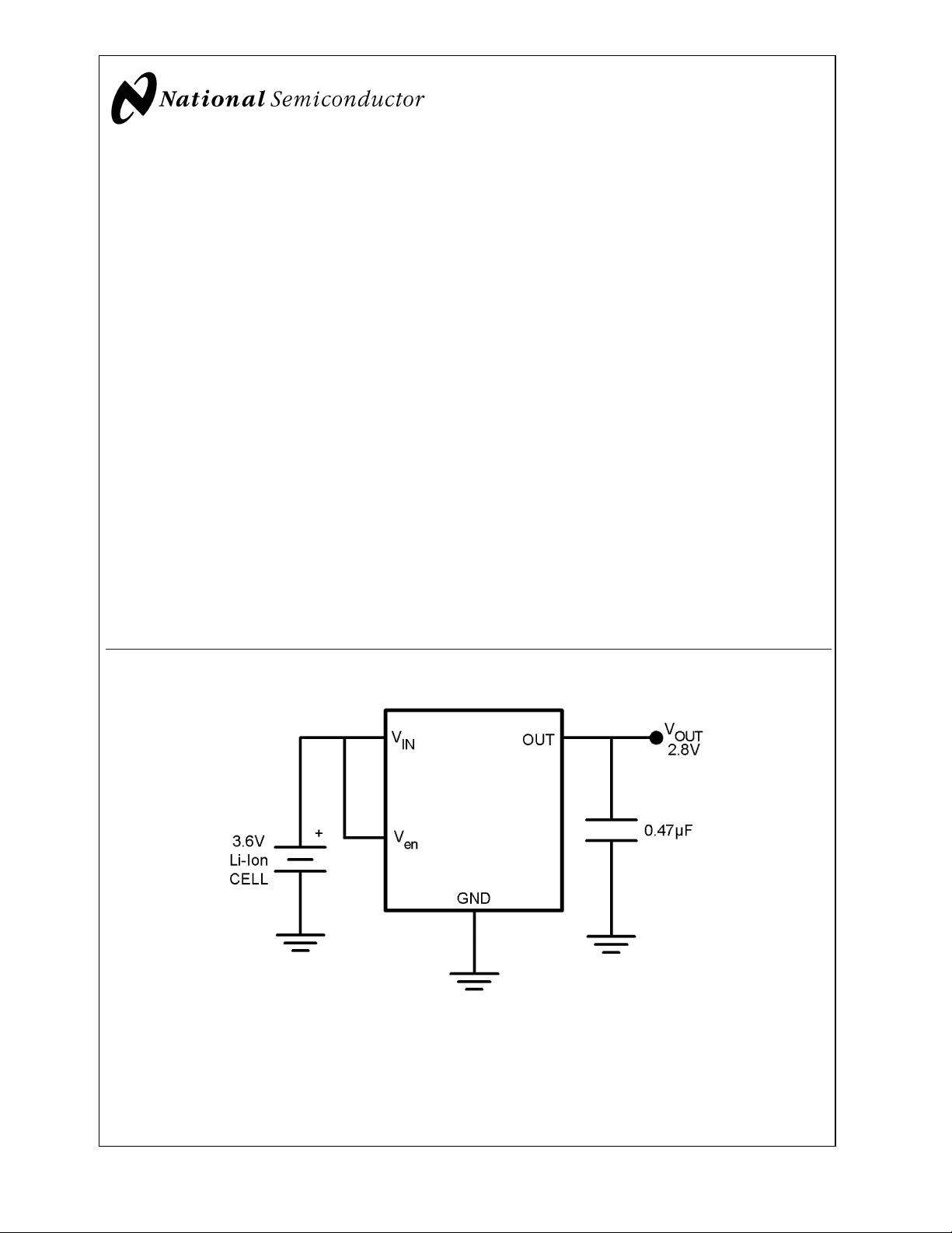
Typical Application
Features
(Typical unless noted)
n Space saving SC70 package
n Low quiescent current: 70µA
n Low dropout voltage: 2mV
n Stability with low-ESR ceramic capacitors
n Auto discharge
n Fast turn-on
n Low temperature coefficient
n Current and thermal limiting
n Zero current in shutdown mode
n Pin-to-pin compatible with LMS5213
Applications
n Cellular Phones
n Battery-powered equipment
n Bar code scanner
n Laptops, notebooks, PDA’s
n High-efficiency linear power supplies
20043120
© 2002 National Semiconductor Corporation DS200431 www.national.com
Page 2
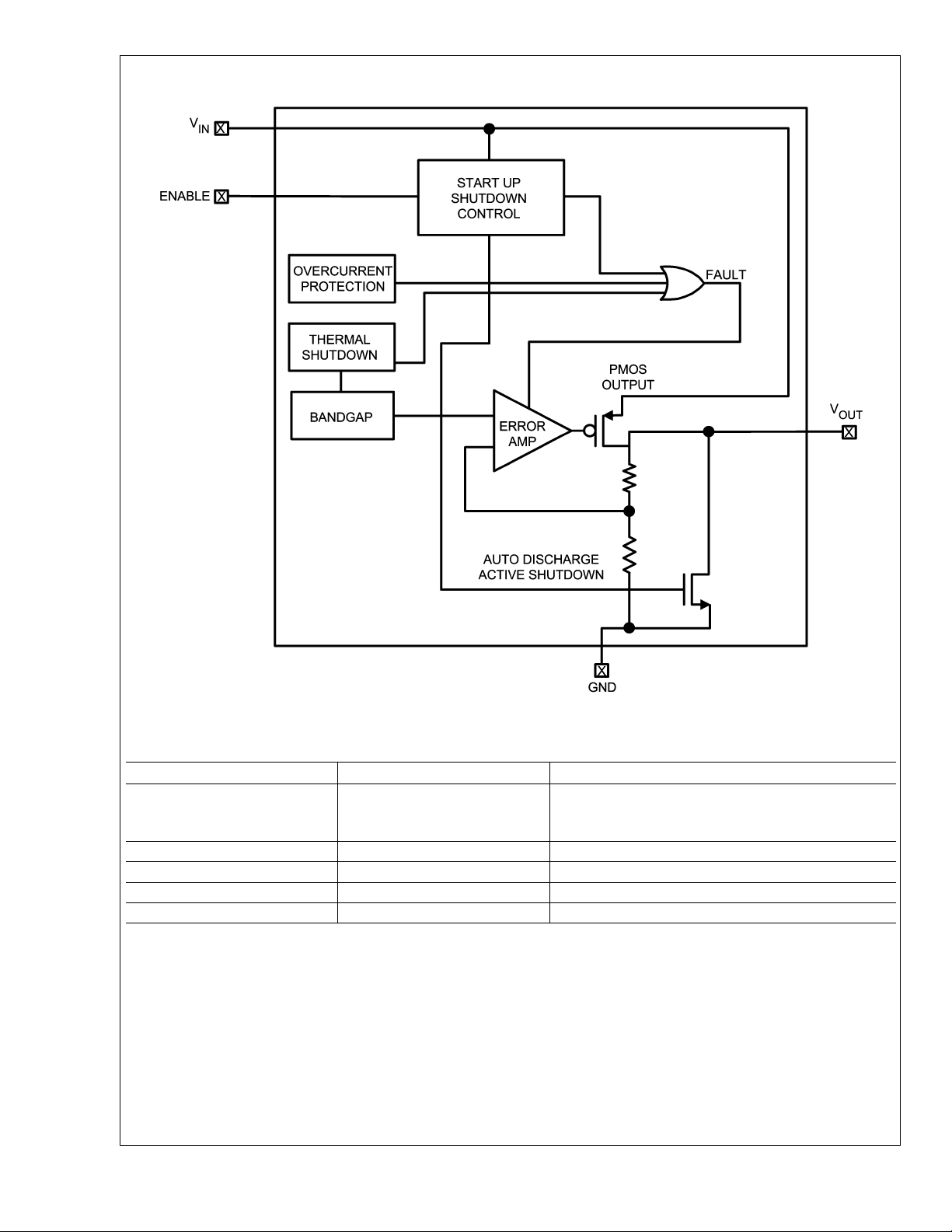
Simplified Schematic
LMS5214
Pin Description
Pin Number Pin Name Pin Function
1V
2 NC Not internally connected
3 GND Ground
4V
5V
EN
OUT
20043101
Enable Input Logic,
Logic High = Enabled
Logic Low = Shutdown
Output Voltage
IN
Input Voltage
www.national.com 2
Page 3
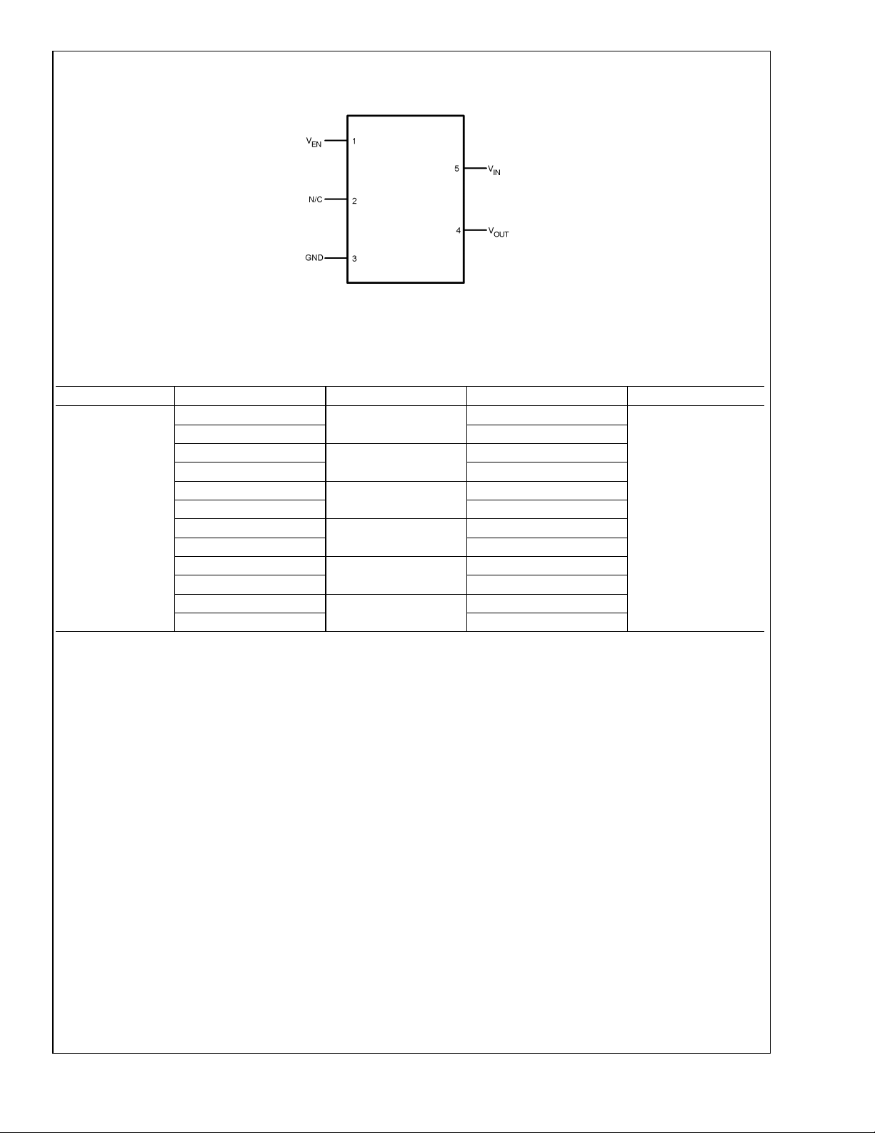
Connection Diagram
LMS5214
SC70-5
Top View
20043121
Ordering Information
(For other output voltage options, please contact National Semiconductor).
Package Part Number Package Marking Transport Media NSC Drawing
5-Pin SC70
LMS5214IMG-2.5
LMS5214IMGX-2.5 3k Units Tape and Reel
LMS5214IMG-2.6
LMS5214IMGX-2.6 3k Units Tape and Reel
LMS5214IMG-2.8
LMS5214IMGX-2.8 3k Units Tape and Reel
LMS5214IMG-2.9
LMS5214IMGX-2.9 3k Units Tape and Reel
LMS5214IMG-3.0
LMS5214IMGX-3.0 3k Units Tape and Reel
LMS5214IMG-3.3
LMS5214IMGX-3.3 3k Units Tape and Reel
L0T
L0U
L0V
L0X
L0Y
L0Z
1k Units Tape and Reel
1k Units Tape and Reel
1k Units Tape and Reel
1k Units Tape and Reel
1k Units Tape and Reel
1k Units Tape and Reel
MAA05A
www.national.com3
Page 4

Absolute Maximum Ratings (Note 1)
If Military/Aerospace specified devices are required,
LMS5214
please contact the National Semiconductor Sales Office/
Distributors for availability and specifications.
ESD Tolerance (Note 2)
Human Body Model 2000V
Machine Model 200V
Junction Temperature 150˚C
V
IN,VOUT,VEN
Soldering Information
Infrared or Convection (20 sec) 235˚C
Wave Soldering (10 sec) 260˚C (lead temp)
−0.3 TO 6.5V
Operating Ratings
Supply Voltages
V
IN
V
EN
Junction Temp. Range (Note 3) −40˚C to +125˚C
Storage Temperature Range −65˚C to 150˚C
Package Thermal Resistance
SC70-5 478˚C/W
Electrical Characteristics
Unless otherwise specified, all limits guaranteed for TJ= 25˚C, VIN=V
≥ 2.0V. Boldface limits apply at the temperature extremes.
V
EN
Symbol Parameter Conditions Min
V
∆V
O
O
Output Voltage Accuracy -3
/∆T Output Voltage Temp.
(Note 10) 50 200 ppm/˚C
Coefficient
∆V
O/VO
∆VO/V
V
IN-VO
I
Q
I
GND
I
LIMIT
∆V
O
Line Regulation VIN=V
Load Regulation IL= 0.1mA to 80mA (Note 6) 0.08 0.3
O
Dropout Voltage
(Note 7)
IL= 100µA 2
I
= 20mA 70 150
L
I
= 50mA 180
L
I
= 80mA 300 500
L
Quiescent Current VEN≤ 0.4V (Shutdown) 10 100 nA
Ground Pin Current IL= 100µA, VEN≥ 2.0V (active) 70
= 20mA, VEN≥ 2.0V (active) 80 135
L
I
= 80mA, VEN≥ 2.0V (active) 110 200
L
Current Limit V
OUT
/∆PDThermal Regulation (Note 9) 0.05 %W
+1V to 6V 0.008 0.3
OUT
= 0V 200 400 mA
Enable Input
V
IL
V
IH
I
IL
I
IH
Note 1: Absolute Maximum Ratings indicate limits beyond which damage to the device may occur. Operating Ratings indicate conditions for which the device is
intended to be functional, but specific performance is not guaranteed. For guaranteed specifications and the test conditions, see the Electrical Characteristics.
Note 2: Human body model, 1.5kΩ in series with 100pF.
Note 3: The maximum power dissipation is a function of T
is P
Note 4: Typical Values represent the most likely parametric norm.
Note 5: All limits are guaranteed by testing or statistical analysis.
Note 6: Regulation is measured at constant junction temperature using low duty cycle pulse testing. Changes in output voltage due to heating effects are covered
by the thermal regulation specification.
Note 7: Dropout voltage is defined as the input to output differential at which the output voltage drops 2% below its nominal value measured at 1V differential.
Note 8: Ground pin current is the regulator quiescent current plus pass transistor base current. The total current drawn from the supply is the sum of the load current
plus the ground pin current.
Note 9: Thermal regulation is defined as the change in output voltage at a time “t” after a change in power dissipation is applied, excluding load or line regulation
effects. Specifications are for an 80mA load pulse at V
Note 10: Output voltage temperature coefficient is defined as the worst-case voltage change divided by the total temperature range.
Enable Input Voltage Level Logic Low (off) 0.6 V
Logic High (on) 2.0 V
Enable Input Current VIL≤ 0.6V 0.01 1 µA
VIH≥ 2.0V 0.01 5 µA
, θJA, and TA. The maximum allowable power dissipation at any ambient temperature
D
=(T
J(MAX)–TA
)/θJA. All numbers apply for packages soldered directly into a PC board.
J(MAX)
= 6V for t = 16ms.
IN
+ 1V, IL= 1mA, CL= 0.47µF,
OUT
(Note 5)
-4
Typ
(Note 4)
Max
(Note 5)
3
4
0.5
0.5
2.5V to 6V
0V to V
Units
%
%
%
mV
µAI
IN
www.national.com 4
Page 5

LMS5214
Typical Characteristics Unless otherwise specified, T
Dropout Voltage vs. Output Current Dropout Voltage vs. Temperature
20043130
Dropout Characteristics Dropout Characteristics
= 25˚C, V
A
= 2.8V, CL= 0.47µF
OUT
20043131
20043109
Ground Current vs. Output Current Ground Current vs. Input Voltage
20043125
20043110
20043127
www.national.com5
Page 6

Typical Characteristics Unless otherwise specified, T
= 25˚C, V
A
= 2.8V, CL= 0.47µF (Continued)
OUT
LMS5214
Ground Current vs. Temperature Short Circuit Current vs. Input Voltage
20043126 20043124
Short Circuit Current vs. Temperature Output Voltage vs. Temperature
20043129
Load Transient Load Transient
20043105
www.national.com 6
20043128
20043106
Page 7

LMS5214
Typical Characteristics Unless otherwise specified, T
Line Transient Ripple Voltage vs. Frequency
20043102
Ripple Voltage vs. Frequency Noise Characteristics
= 25˚C, V
A
= 2.8V, CL= 0.47µF (Continued)
OUT
20043132
20043133
Enable Characteristics Start Up Characteristics
20043107 20043103
20043108
www.national.com7
Page 8

Typical Characteristics Unless otherwise specified, T
= 25˚C, V
A
= 2.8V, CL= 0.47µF (Continued)
OUT
LMS5214
Application Information
The LMS5214 is a low dropout, linear regulator designed
primarily for battery-powered applications. The LMS5214
can be used with low cost ceramic capacitors, typical value
of 470nF.
The LMS5214 is an enhanced version of the LMS5213 with
auto discharge function which actively discharges the output
voltage to ground when the device is placed in shutdown
mode
As illustrated in the simplified schematics, the LMS5214
consists of a 1.25V reference, error amplifier, P-channel
pass transistor and internal feedback voltage divider. The
1.25V reference is connected to the input of the error amp.
The error amp compares this reference with the feedback
voltage. If the feedback voltage is lower than the reference,
the pass transistor gate is pulled lower allowing more current
to pass and increasing the output voltage. If the feedback
voltage is too high, the pass transistor gate is pulled up
allowing less current to pass to the output. The output voltage is fedback through the resistor divider. Additional blocks
include short circuit current protection and thermal protection.
The LMS5214 features an 80mA P-channel MOSFET transistor. This provides several advantages over similar designs
using PNP pass transistors including longer battery life.
The P-channel MOSFET requires no base drive, which reduces quiescent current considerably. PNP based regulators
waste considerable amounts of current in dropout when the
pass transistor saturates. They also have high base drive
currents under large loads. The LMS5214 does not suffer
from these problems and consumes only the specified quiescent current under light and heavy loads.
External Capacitors
Like any low-dropout regulators, the LMS5214 requires external capacitors for regulator stability. The LMS5214 is specially designed for portable applications requiring minimum
board space and the smallest components.
A 1µF capacitor should be placed from V
more than 10 inches of wire between the input and AC filter
or when a battery is used as the input. This capacitor must
be located a distance of not more than 1cm from the input
pin and returned to a clean analog ground.
to GND if there is
IN
Start Up Characteristics
The LMS5214 is designed to work with high quality tantalum
capacitors and small ceramic output capacitors. Ceramic
capacitors ranging between 470nF to 4.7µF are the smallest
and least expensive.
No-Load Stability
The LMS5214 will remain stable and in regulation with
no-load (other than the internal voltage divider). This is
especially important in CMOS RAM keep-alive applications.
Enable Input
The LMS5214 is shut off by pulling the V
all internal circuitry is powered off and the quiescent current
is typically 10nA. Pulling the V
the device and allows operation. If the shut down feature is
not used, the V
regulator output on all the time.
Thermal Behavior
The LMS5214 regulator has internal thermal shutdown to
protect the device from over heating. Under all operating
conditions, the maximum junction temperature of the
LMS5214 must be below 125˚C. Maximum power dissipation
can be calculated based on the output current and the
voltage drop across the part. The maximum power dissipation is
P
θJAis the junction-to-ambient thermal resistance, 478˚C/W
for the LMS5214 in the SC70 package. T
ambient temperature T
perature of the die, 125˚C
When operating the LMS5214 at room temperature, the
maximum power dissipation is 209mW.
The actual power dissipated by the regulator is
P
The figure below shows the voltage and currents, which are
present in the circuit.
D(MAX)
=(VIN-V
D
20043104
EN
high above 2V re-enables
EN
pin should be tied to VINto keep the
EN
=(T
J(MAX)-TA
OUT)IL+VINIGND
)/θ
JA
is the maximum junction tem-
J(MAX)
A
pin below 0.6V;
is the maximum
www.national.com 8
Page 9

Application Information (Continued)
20043122
FIGURE 1. Power Dissipation Diagram
LMS5214
Fixed Voltage Regulator
The LMS5214 offers a smaller system solution that is ideal
for general-purpose voltage regulation in any handheld device.
Substituting P
, determined above, for PDand solving
D(MAX)
for the operating condition that are critical to the application
will give the maximum operating conditions for the regulator
circuit. To prevent the device from entering thermal shutdown, maximum power dissipation cannot be exceeded.
20043120
FIGURE 2. Single-Cell Regulator
www.national.com9
Page 10

Physical Dimensions inches (millimeters) unless otherwise noted
5-Pin SC70-5
NSC Package Number MAA05A
LIFE SUPPORT POLICY
NATIONAL’S PRODUCTS ARE NOT AUTHORIZED FOR USE AS CRITICAL COMPONENTS IN LIFE SUPPORT
DEVICES OR SYSTEMS WITHOUT THE EXPRESS WRITTEN APPROVAL OF THE PRESIDENT AND GENERAL
COUNSEL OF NATIONAL SEMICONDUCTOR CORPORATION. As used herein:
1. Life support devices or systems are devices or
systems which, (a) are intended for surgical implant
into the body, or (b) support or sustain life, and
whose failure to perform when properly used in
accordance with instructions for use provided in the
2. A critical component is any component of a life
support device or system whose failure to perform
can be reasonably expected to cause the failure of
the life support device or system, or to affect its
safety or effectiveness.
labeling, can be reasonably expected to result in a
LMS5214 80mA, Low Dropout Voltage Regulator with Auto Discharge Function in SC70
significant injury to the user.
National Semiconductor
Corporation
Americas
Email: support@nsc.com
www.national.com
National Semiconductor
Europe
Fax: +49 (0) 180-530 85 86
Email: europe.support@nsc.com
Deutsch Tel: +49 (0) 69 9508 6208
English Tel: +44 (0) 870 24 0 2171
Français Tel: +33 (0) 1 41 91 8790
National Semiconductor
Asia Pacific Customer
Response Group
Tel: 65-2544466
Fax: 65-2504466
Email: ap.support@nsc.com
National Semiconductor
Japan Ltd.
Tel: 81-3-5639-7560
Fax: 81-3-5639-7507
National does not assume any responsibility for use of any circuitry described, no circuit patent licenses are implied and National reserves the right at any time without notice to change said circuitry and specifications.
 Loading...