

Page 1
LMS202E
15KV ESD Rated, 5V Single Supply TIA/EIA-232 Dual
Transceivers
LMS202E 15KV ESD Rated, 5V Single Supply TIA/EIA-232 Dual Transceivers
March 2003
General Description
The LMS202E features two transmitters and two receivers
for RS-232 communication. It has a DC-to-DC converter that
permits the device to operate with only a single +5V power
supply. The on-chip DC-to-DC converter which utilizes four
external 0.1µF capacitors to generate dual internal power
supplies for RS-232 compatible output levels.
The device meet EIA/TIA-232E and CCITT V.28 specifications up to 230kbits/sec. The LMS202E is available in a 16
pin narrow and wide SOIC package.
±
The transmitter outputs and receiver inputs have
electrostatic discharge (ESD) protection. The LMS202E survives a
pins when subjected according to Human Body Model or IEC
1000-4-2 (EN61000-4-2),air-gap specification. It survives a
±
4-2), contact specification. This device is designed for use in
harsh environments where ESD is a concern.
±
15kV ESD event to the RS-232 input and output
8kV discharge when subjected to IEC 1000-4-2 (EN61000-
15kV
Features
n ESD protection for RS-232 I/O pins
n Single +5V power supply
n 230 kbps data rate
n On-board DC-to-DC converter
n 0.1µF charge pump capacitors
n Drop-in replacement to Maxim’s MAX202E
Applications
n POS equipment (Bar code reader)
n Hand-held equipment
n General purpose RS-232 communication
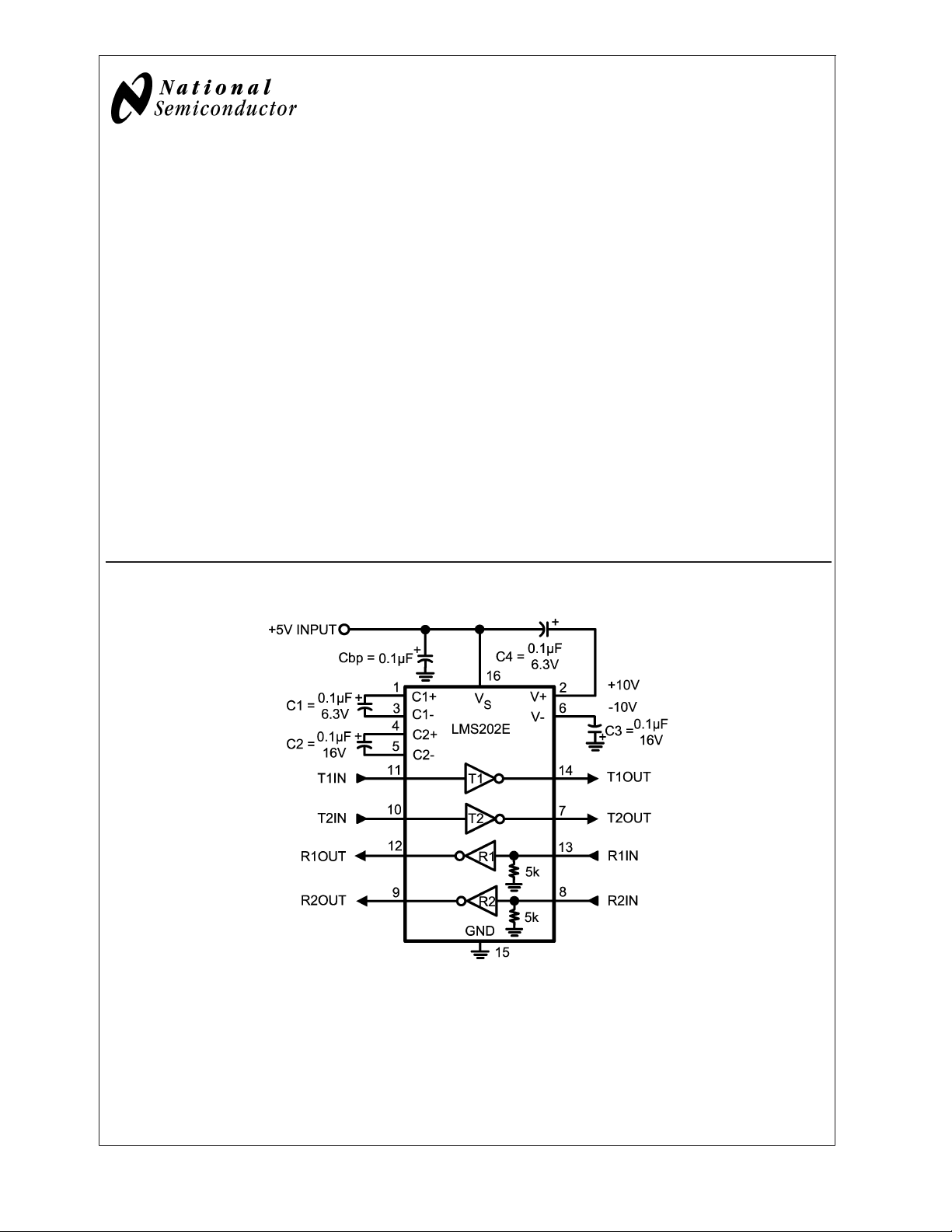
Connection Diagram and Typical Circuit
±
15kV-IEC1000 4-2 (EN61000-4-2) Contact
—
Discharge
±
8kV-IEC1000 4-2 (EN61000-4-2) Air-Gap Discharge
—
±
15kV Human Body Model
—
20048001
© 2003 National Semiconductor Corporation DS200480 www.national.com
Page 2
Pin Descriptions
Pin Number Pin Name Pin Function
LMS202E
1, 3 C1+, C1− External capacitor connection pins. Recommended external capacitor C1 = 0.1µF (6.3V)
2 V+ Positive supply for TIA/EIA-232E drivers. Recommended external capacitor C4 = 0.1µF (6.3V)
4, 5 C2+, C2− External capacitor connection pins. Recommended external capacitor C2 = 0.1µF (16V)
6 V− Negative supply for TIA/EIA-232E drivers. Recommended external capacitor C3 = 0.1µF (16V)
7, 14 T1out, T2out Transmitter output pins conform to TIA/EIA-232E levels. The typical transmitter output swing is
±
8V when loaded 3kΩ load to ground. The open-circuit output voltage swings from (V+ − 0.6V)
to V−
8,13 R1in, R2in Receiver inputs accept TIA/EIA-232
9, 12 R1out and R2out Receiver output pins are TTL/CMOS compatible
10, 11 Tin1, Tin2 Transmitter input pins are TTL/CMOS compatible. Inputs of transmitter do not have pull-up
resistors. Connect all unused transmitter inputs to ground
15 GND Ground pin
16 V
S
Power supply pin for the device, +5V (±10%)
Ordering Information
Package Part Number Package Marking Transport Media NSC Drawing
16-Pin SOIC
16-Pin Wide SOIC
LMS202ECM
LMS202ECMX 2.5k Units Tape and Reel
LMS202EIM
LMS202EIMX 2.5k Units Tape and Reel
LMS202ECMW
LMS202ECMWX 1.0k Units Tape and Reel
LMS202EIMW
LMS202EIMWX 1.0k Units Tape and Reel
LMS202ECM
LMS202EIM
LMS202ECMW
LMS202EIMW
48 Units/Rail
48 Units/Rail
45 Units/Rail
45 Units/Rail
M16A
M16B
www.national.com 2
Page 3
LMS202E
Absolute Maximum Ratings (Note 1)
If Military/Aerospace specified devices are required,
please contact the National Semiconductor Sales Office/
Distributors for availability and specifications.
V
S
V+ (V
V− +0.3V to −14V
Driver Input Voltage, T
IN
Receiver Input Voltage, R
Driver Output Voltage T
O
Receiver Output Voltage R
Short Circuit Duration, T
O
IN
O
−0.3V to (V+ +0.3V)
(V− −0.3V to (V+ + 0.3V)
ESD Rating
IEC 1000-4-2) (Note 7)
(Note 8)
Air-Gap Discharge 15kV
Contact Discharge 8kV
Human Body Model (Note 2)
−0.3V to 6V
− 0.3V) to + 14V
S
±
−0.3 to (VS+ 0.3)
Continuous
30V
(Note 9) 2kV
ESD Rating (MM) 200V (Note 6) (Note 9)
Soldering Information
Infrared or Convection 235˚C
(20sec.)
Junction Temperature 150˚C
Storage Temperature Range −65˚C to +150˚C
Operating Ratings
Supply Voltage V
Ambient Temperature Range, T
S
A
Commercial (C) 0˚C to +70˚C
Industrial (I) −40˚C to +85˚C
Package Thermal Resistance
(Note 3)
SO 71˚C/W
WSO 55˚C/W
4.5V to 5.5V
(Note 8) 15kV
Electrical Characteristics
Over recommended operating supply and temperature ranges unless otherwise specified C1 = C2 = C3 = C4 = Cbp = 0.1µF
Symbol Parameter Conditions Min
(Note 5)
DC Characteristics
I
S
Supply Current No Load, TA= 25˚C 1 7 mA
Logic
I
INPUT
V
THL
V
THH
V
OL
Input Leakage Current TIN=0VtoV
Input Logic Theshold Low T
Input Logic Theshold High T
TTL/CMOS Output Voltage
IN
IN
R
OUT,IOUT
= 3.2mA 0.4 V
S
Low
V
OH
TTL/CMOS Output Voltage
R
OUT,IOUT
= −1.0mA 3.5 VS−0.1 V
High
RS-232 Receiver Inputs
V
RI
Receiver Input Voltage
Range
V
RTHL
Receiver Input Theshold
VS= 5V, TA= 25˚C 0.8 1.4 V
Low
V
RTHH
Receiver Input Theshold
VS= 5V, TA= 25˚C 2 2.4 V
High
V
R
HYST
I
Receiver Input Hysteresis VS= 5V 0.2 0.6 1.0 V
Receiver Input Resistance VS= 5V, TA= 25˚C 3 5 7 kΩ
RS-232 Transmitter Outputs
V
O
Transmitter Output Voltage
All transmitters loaded with 3kΩ to GND
Swing
R
O
I
OS
Output Resistance VS=V+=V−=0V,
=±2V
V
O
Output Short Circuit Current
Timing Characteristics
DR Maximum Data Rate C
= 50pF to 1000pF,
L
=3kΩ to 7kΩ
R
L
2.0 V
−30 +30 V
±
5
300 Ω
230 kbps
Typ Max
(Note 5)
±
10 µA
0.8 V
±
8V
±
11
±
60 mA
Units
www.national.com3
Page 4

Electrical Characteristics (Continued)
Over recommended operating supply and temperature ranges unless otherwise specified C1 = C2 = C3 = C4 = Cbp = 0.1µF
LMS202E
Symbol Parameter Conditions Min
(Note 5)
T
T
T
T
V
RPLH
RPHL
DPLH
DPHL
SLEW
Receiver Propagation Delay CL= 150pF 0.08 1 µs
Transmitter Propagation
Delay
Transition Region Slew Rate TA= 25˚C, VS=5V
RL=3kΩ,CL= 2500pF
All transmitters loaded
= 50pF to 1000pF, RL=3kΩ to 7kΩ
C
L
3 6 30 V/µs
Measured from +3V to −3V or vice versa
ESD Performance: Transmitter Outputs and Receiver Inputs
ESD Rating Human Body Model
IEC 1000-4-2, Contact
IEC 1000-4-2, Air-gap
Note 1: Absolute Maximum Ratings indicate limits beyond which damage to the device may occur. Operating Ratings indicate conditions for which the device is
intended to be functional, but specific performance is not guaranteed. For guaranteed specifications and the test conditions, see the Electrical Characteristics.
Note 2: Human Body Model, 1.5kΩ in series with 100pF
Note 3: The maximum power dissipation is a function of T
(T
J(MAX)−TA
Note 4: Typical Values represent the most likely parametric norm.
Note 5: All limits are guaranteed by testing or statistical analysis
Note 6: Machine model, 0Ω in series with 200pF
Note 7: IEC 1000-4-2, 330Ω in series with 150pF
Note 8: ESD rating applies to pins 7,8 13 and 14
Note 9: ESD rating applies to pins 1, 2, 3, 4, 5, 6, 9, 10, 11, 12, 15 and 16
)/ θ
All numbers apply for packages soldered directly onto a PC board.
JA.
J(MAX),θJA,
and TA.The maximum allowable power dissipation at any ambient temperature is PD=
Typ Max
(Note 5)
2.4 µs
±
15 kV
±
8
±
15
Units
www.national.com 4
Page 5

Typical Characteristics
Transmitter Output High Voltage vs. Load Capacitance Transmitter Slew Rate vs. Load Capacitance
20048002 20048003
LMS202E
Application Information
CAPACITOR SELECTION
The recommended capacitors are 0.1µF. However, larger
capacitors for the charge pump may be used to minimized
ripples on V+ and V− pins.
POWER SUPPLY DECOUPLING
In some applications that are sensitive to power supply noise
from the charge pump, place a decoupling capacitor, Cbp,
from V
size as the charge pump capacitors (C1 − C4).
CHARGED PUMP
The dual internal charged-pump provides the
transmitters. Using capacitor C1, the charge pump converts
+5V to +10V then stores the +10V in capacitor C3. The
charge pump uses capacitor C2 to invert the +10V to −10V.
The −10V is then stored in capacitor C4.
ELECTROSTATIC DISCHARGE PROTECTION
ESD protection has been placed at all pins to protect the
device from ESD. All pins except for the transmitter output
pins (pins 7 and 14) and receiver input pins (pins 8 and 13)
have a ESD rating of 2kV Human Body Model (HBM) and
200V Machine Model (MM). The RS-232 bus pins (pins 7, 8,
13 and 14) have a more robust ESD protection. The RS-232
bus pins have a ESD rating of 15kV HBM and IEC 1000-4-2,
air-gap. In addition the bus pins meet an ESD rating of 8kV
with IEC 1000-4-2, contact. The ESD structures can withstand a high ESD event under the following conditions:
powered-on, powered-off, and Input connected to high and
low with outputs unloaded.
to GND. Use at least a 0.1µF capacitor or the same
S
±
10V to the to
pacitor through a resistor, R2 = 1.5 kΩ. The peak current is
approximately 1.33A.
20048004
FIGURE 1. HBM ESD Test Model
HUMAN BODY MODEL
The Human Body Model is an ESD testing standard, defined
in Mil-STD-883C method 3015.7. It simulates a human discharging an ESD charge to the IC device. The rise time is
approximately 10 ns and decay time is approximately 150
ns. The waveform is obtained by discharging 2kV volts ca-
20048005
FIGURE 2. HBM Waveform
www.national.com5
Page 6

Application Information (Continued)
MACHINE MODEL
LMS202E
The Machine Model is the standard ESD test method in
Japan and the automotive industry. It simulates a charge on
large object discharging through the IC device. This takes
place in automated test and handling systems. The equipment can accumulate static charge due to improper grounding, which is transmitted through the IC when it is picked and
placed.
The waveform is obtained by discharging 400V volts capacitor to the device. Resistor, R2 = 0Ω.
The parasitic inductance, L, from the PCB affects the peak
current and period of the waveform. For L = 0.5µF, the peak
current is approximately 7A with a period of 60 ns. For L =
2.5µH, the peak current is reduced to 4A with a period of 140
ns.
IEC 1000-4-2 (EN61000-4-2)
The European Union requires ESD immunity testing for all
electronic products as a condition for EMC Mark before
shipping to any member countries. This is not a IC requirement but an overall system requirement. IEC 1000-4-2
specifies ESD testing both by contact and air-gap discharge.
ESD testing by contact are generally more repeatable than
air-gap but is less realistic to actual ESD event. However,
air-gap discharge is more realistic but ESD results may vary
widely dependent on environmental conditions (temperature,
humidity,....) The waveform is obtained by discharging
150pF capacitor through a resistor, R2 = 330Ω. A typical
peak current may be high as 37A with 10kV.
20048004
FIGURE 5. IEC ESD Model
FIGURE 3. MM ESD Model
FIGURE 4. MM Waveform
20048004
20048007
20048009
FIGURE 6. IEC Waveform
www.national.com 6
Page 7

Physical Dimensions inches (millimeters) unless otherwise noted
16-Pin SOIC
NS Package Number M16A
LMS202E
16-Pin Wide SOIC
NS Package Number M16B
www.national.com7
Page 8

Notes
LIFE SUPPORT POLICY
NATIONAL’S PRODUCTS ARE NOT AUTHORIZED FOR USE AS CRITICAL COMPONENTS IN LIFE SUPPORT
DEVICES OR SYSTEMS WITHOUT THE EXPRESS WRITTEN APPROVAL OF THE PRESIDENT AND GENERAL
COUNSEL OF NATIONAL SEMICONDUCTOR CORPORATION. As used herein:
LMS202E 15KV ESD Rated, 5V Single Supply TIA/EIA-232 Dual Transceivers
1. Life support devices or systems are devices or
systems which, (a) are intended for surgical implant
into the body, or (b) support or sustain life, and
whose failure to perform when properly used in
accordance with instructions for use provided in the
2. A critical component is any component of a life
support device or system whose failure to perform
can be reasonably expected to cause the failure of
the life support device or system, or to affect its
safety or effectiveness.
labeling, can be reasonably expected to result in a
significant injury to the user.
National Semiconductor
Americas Customer
Support Center
Email: new.feedback@nsc.com
Tel: 1-800-272-9959
www.national.com
National does not assume any responsibility for use of any circuitry described, no circuit patent licenses are implied and National reserves the right at any time without notice to change said circuitry and specifications.
National Semiconductor
Europe Customer Support Center
Fax: +49 (0) 180-530 85 86
Email: europe.support@nsc.com
Deutsch Tel: +49 (0) 69 9508 6208
English Tel: +44 (0) 870 24 0 2171
Français Tel: +33 (0) 1 41 91 8790
National Semiconductor
Asia Pacific Customer
Support Center
Fax: +65-6250 4466
Email: ap.support@nsc.com
Tel: +65-6254 4466
National Semiconductor
Japan Customer Support Center
Fax: 81-3-5639-7507
Email: jpn.feedback@nsc.com
Tel: 81-3-5639-7560
 Loading...