

Datasheet LMS1587IT-ADJ, LMS1587IT-3.3, LMS1587ISX-3.3, LMS1587IS-ADJ, LMS1587IS-3.3 Datasheet (NSC)
...Page 1
LMS1585A/LMS1587
5A and 3A Low Dropout Fast Response Regulators
LMS1585A/LMS1587 5A Low Dropout Fast Response Regulators
April 2000
General Description
The LMS1585AandLMS1587arelowdropoutpositiveregulators with output load current of 5A and 3A respectively.
Their low dropout voltage (1.2V) and fast transient response
make them an excellent solution for low voltage microprocessor applications.
The LMS1585A/87 are available in adjustable versions,
which can set the output voltage with only two external resistors. In addition, they are also available in a 3.3V fixed voltage version (Note 9).
The LMS1585A/87 circuits include a zener trimmed bandgap
reference, current limiting and thermal shutdown.
The LMS1585A/87 series are available in TO-220 and TO263 packages.
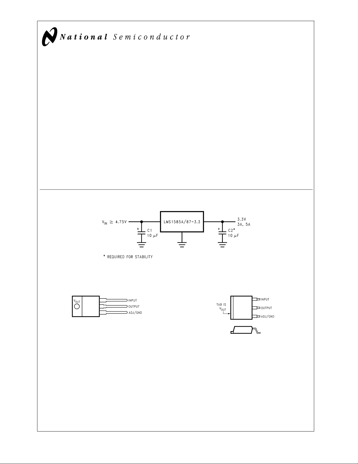
Typical Application
Features
n Fast transient response
n Available in Adjustable, 1.5V, and 3.3V versions
n Current limiting and thermal protection
n Commercial temp. range 0˚C to 125˚C
n Industrial temp. range −40˚C to 125˚C
n Line regulation 0.005% (typical)
n Load regulation 0.05% (typical)
n Direct replacement for LT
™
1585A/87
Applications
n Pentium™processor supplies
n PowerPC
n Other 2.5V to 3.6V microprocessor supplies
n Low voltage logic supplies
™
supplies
Connection Diagrams
TO-220
Top View
LT is a registered trademark of Linear Technology Corporation
Pentium is a registered trademark of Intel Corporation
PowerPC is a registred trademark of IBM
DS101197-1
TO-263
DS101197-36
DS101197-35
Top View
© 2000 National Semiconductor Corporation DS101197 www.national.com
Page 2
Ordering Information
Output
Current
3A TO-263 0˚C to 125˚C LMS1587CS-ADJ Rails
LMS1585A/LMS1587
5A TO-263 0˚C to 125˚C LMS1585ACS-ADJ Rails
Package Temperature Range Part Number Transport Media NSC
LMS1587CSX-ADJ Tape and Reel
LMS1587CS-1.5 Rails
LMS1587CSX-1.5 Tape and Reel
LMS1587CS-3.3 Rails
LMS1587CSX-3.3 Tape and Reel
−40˚C to 125˚C LMS1587IS-ADJ Rails
LMS1587ISX-ADJ Tape and Reel
LMS1587IS-3.3 Rails
LMS1587ISX-3.3 Tape and Reel
TO-220 0˚C to 125˚C LMS1587CT-ADJ Rails
LMS1587CT-3.3 Rails
−40˚C to 125˚C LMS1587IT-ADJ Rails
LMS1587IT-3.3 Rails
LMS1585ACSX-ADJ Tape and Reel
LMS1585ACS-3.3 Rails
LMS1585ACSX-3.3 Tape and Reel
−40˚C to 125˚C LMS1585AIS-ADJ Rails
LMS1585AISX-ADJ Tape and Reel
LMS1585AIS-3.3 Rails
LMS1585AISX-3.3 Tape and Reel
TO-220 0˚C to 125˚C LMS1585ACT-ADJ Rails
LMS1585ACT-3.3 Rails
−40˚C to 125˚C LMS1585AIT-ADJ Rails
LMS1585AIT-3.3 Rails
Drawing
TS3B
T03B
TS3B
T03B
www.national.com 2
Page 3
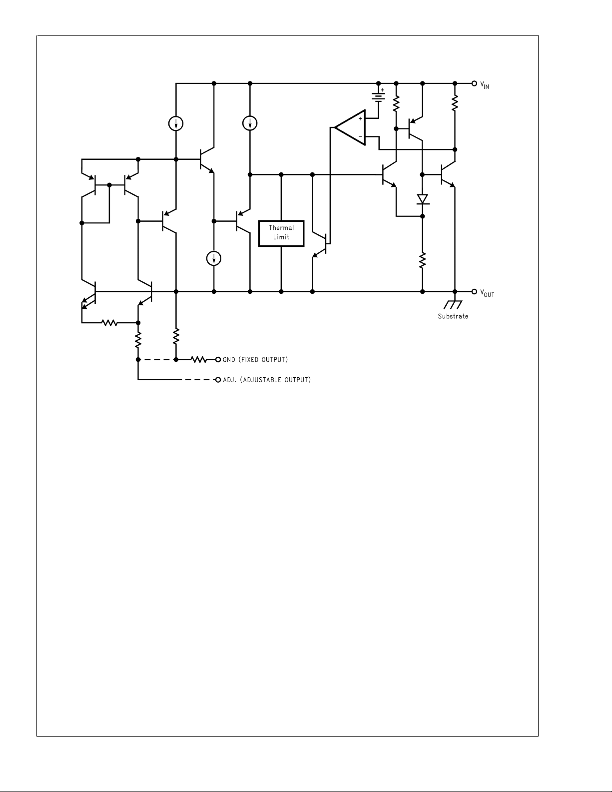
Simplified Schematic
LMS1585A/LMS1587
DS101197-14
www.national.com3
Page 4

Absolute Maximum Ratings (Note 1)
If Military/Aerospace specified devices are required,
please contact the National Semiconductor Sales Office/
Distributors for availability and specifications.
Maximum Input to Output Voltage
(V
to GND) 13V
IN
Power Dissipation (Note 2) Internally Limited
Junction Temperature (T
)(Note 2) 150˚C
J
Storage Temperature Range -65˚C to 150˚C
Lead Temperature 260˚C, 10 sec
ESD Tolerance (Note 3) 2000V
LMS1585A/LMS1587
Electrical Characteristics
Typicals and limits appearing in normal type apply for TJ= 25˚C. Limits appearing in Boldface type apply over the entire junction temperature range for operation, 0˚C to 125˚C for commercial grade and −40˚C to 125˚C for industrial grade.
Symbol Parameter Conditions
V
REF
Reference Voltage LMS1585A-ADJ
V
IN−VOUT
10mA ≤ I
= 3V, I
≤ 5A, 1.5V ≤ VIN−V
OUT
OUT
= 10mA
LMS1587-ADJ
10mA ≤ I
V
OUT
Output Voltage LMS1585A-3.3
= 0mA, VIN=5V
I
OUT
0≤I
OUT
≤ 3A, 1.5V ≤ VIN−V
OUT
≤ 5A, 4.75V ≤ VIN≤ 7V
LMS1587-1.5
V
IN
0≤ I
= 5V, I
OUT
= 0mA, TJ= 25˚C
OUT
≤ 3A, 3V ≤ VIN≤ 7V
LMS1587-3.3
∆V
OUT
Line Regulation
(Note 6)
0 ≤ I
LMS1585A/87-ADJ
I
OUT
≤ 3A, 4.75V ≤ VIN≤ 7V 3.235 3.300 3.365 V
OUT
= 10mA, 2.75V ≤ VIN≤ 7V 0.005 0.2 %
LMS1585A/87-3.3
I
= 0mA, 4.75V ≤ VIN≤ 7V 0.005 0.2 %
OUT
LMS1587-1.5
I
= 0mA, 3V ≤ VIN≤ 7V 0.005 0.2 %
OUT
∆V
OUT
Load Regulation
(Note 6)
LMS1585A-ADJ
V
IN−VOUT
= 3V, 10mA ≤ I
LMS1585A-3.3
V
= 5V, 0 ≤ I
IN
OUT
≤ 5A
LMS1587-ADJ
V
IN−VOUT
= 3V, 10mA ≤ I
LMS1587-1.5
V
= 5V, 0 ≤ I
IN
OUT
≤ 3A
LMS1587-3.3
V
V
IN−VOUT
= 5V, 0 ≤ I
IN
Dropout Voltage LMS1585A-ADJ/LMS1587-ADJ
= 1%, I
∆V
REF
≤ 3A
OUT
= 3A 1.15 1.3 V
OUT
LMS1585A-3.3/LMS1587-3.3/LMS1587-1.5
∆V
OUT
= 1%, I
= 3A 1.15 1.3 V
OUT
LMS1585A-ADJ
∆V
REF
= 1%, I
= 5A 1.2 1.4 V
OUT
LMS1585A-3.3
∆V
I
LIMIT
= 1%, I
OUT
Current Limit LMS1585A-ADJ/LMS1585A-3.3
V
IN−VOUT
= 5.5V 5.0 6.6 A
= 5A 1.2 1.4 V
OUT
LMS1587-ADJ/LMS1587-3.3
V
IN−VOUT
= 5.5V 3.1 4.3 A
LMS1587-1.5
V
IN−VOUT
= 5.5V 3.100 3.750 A
OUT
OUT
Min
(Note
5)
1.238
≤ 5.75V
OUT
≤ 5.75V 1.225 1.250 1.275 V
OUT
1.225
3.267
3.235
1.485
1.470
≤ 5A
≤ 3A
Typ
(Note
4)
1.25
1.250
3.300
3.300
1.500
1.500
0.05
0.05
0.05
0.05
0.05
0.05
0.05
0.05
0.05
0.05
Max
(Note5)Units
1.262
1.275
3.333
3.365
1.515
1.530
V
V
V
V
V
V
0.3
0.5 %
0.3
0.5 %
0.3
0.5 %
0.3
0.5
%
%
0.3
0.5 %
www.national.com 4
Page 5

Electrical Characteristics (Continued)
Typicals and limits appearing in normal type apply for TJ= 25˚C. Limits appearing in Boldface type apply over the entire junction temperature range for operation, 0˚C to 125˚C for commercial grade and −40˚C to 125˚C for industrial grade.
Symbol Parameter Conditions
(Note
5)
Min
Minimum Load
Current (Note 7)
LMS1585A/87-ADJ
1.5V ≤ V
IN−VOUT
≤ 5.75V 2.0 10.0 mA
Quiescent Current LMS1585A-3.3/LMS1587-3.3/LMS1587-1.5
V
= 5V 7.0 13.0 mA
IN
Thermal Regulation T
= 25˚C, 30ms Pulse 0.003 %/W
A
Ripple Rejection LMS1585A-ADJ
f
= 120Hz, VIN−V
RIPPLE
= 25µF Tantalum 72 dB
C
OUT
OUT
= 3V, I
OUT
=5A
LMS1585-3.3
f
= 120Hz, C
RIPPLE
= 5A, VIN= 6.3V 72 dB
I
OUT
= 25µF Tantalum,
OUT
LMS1587-ADJ
f
= 120Hz, VIN−V
RIPPLE
= 25µF Tantalum 72 dB
C
OUT
OUT
= 3V, I
OUT
=3A
LMS1587-1.5
f
= 120Hz, C
RIPPLE
= 3A, VIN= 4.5V 60 72 dB
I
OUT
= 25µF Tantalum,
OUT
LMS1587-3.3
f
= 120Hz, C
RIPPLE
= 3A, VIN= 6.3V 72 dB
I
OUT
= 25µF Tantalum,
OUT
Adjust Pin Current 55 120 µA
Adjust Pin Current 10mA ≤ I
1.5V ≤ V
≤ I
OUT
IN−VOUT
FULLLOAD
,
≤ 5.75V (Note 8) 0.2 µA
Temperature Stability 0.5 %
Long Term Stability T
RMS Output Noise
(% of V
OUT
)
Thermal Resistance
Junction-to-Case
Note 1: Absolute Maximum Ratings indicate limits beyond which damage to the device may occur. Operating Ratings indicate conditions for which the device is intended to be functional, but specific performance is not guaranteed. For guaranteed specifications and the test conditions, see the Electrical Characteristics.
Note 2: The maximum power dissipation is a function of T
=(T
is P
D
J(max)–TA
Note 3: For testing purposes, ESD was applied using human body model, 1.5kΩ in series with 100pF.
Note 4: Typical Values represent the most likely parametric norm.
Note 5: All limits are guaranteed by testing or statistical analysis.
Note 6: Load and line regulation are measured at constant junction temperature, and are guaranteed up to the maximum power dissipation of 30W. Power dissipa-
tion is determined by the input/output differential and the output current. Guaranteed maximum power dissipation will not be available over the full input/output range.
Note 7: The minimum output current required to maintain regulation.
Note 8: I
FULLLOAD
Note 9: Consult factory for other fixed voltage options.
)/θJA. All numbers apply for packages soldered directly into a PC board.
is 5A for LMS1585A and 3A for LMS1587.
= 125˚C, 1000Hrs 0.03 %
A
10Hz ≤ f ≤ 10kHz 0.003 %
3-Lead TO-263: Control/Output Section
3-Lead TO-220: Control/Output Section
, θJA, and TA. The maximum allowable power dissipation at any ambient temperature
J(max)
Typ
(Note
4)
Max
(Note5)Units
0.65/2.7
0.65/2.7
˚C/W
˚C/W
LMS1585A/LMS1587
www.national.com5
Page 6

Physical Dimensions inches (millimeters) unless otherwise noted
LMS1585A/LMS1587
3-Lead TO-263 Package
NSC Package Number TS3B
www.national.com 6
Page 7

Physical Dimensions inches (millimeters) unless otherwise noted (Continued)
LMS1585A/LMS1587 5A Low Dropout Fast Response Regulators
3-Lead TO-220 Package
NSC Package Number T03B
LIFE SUPPORT POLICY
NATIONAL’S PRODUCTS ARE NOT AUTHORIZED FOR USE AS CRITICAL COMPONENTS IN LIFE SUPPORT
DEVICES OR SYSTEMS WITHOUT THE EXPRESS WRITTEN APPROVAL OF THE PRESIDENT AND GENERAL
COUNSEL OF NATIONAL SEMICONDUCTOR CORPORATION. As used herein:
1. Life support devices or systems are devices or
systems which, (a) are intended for surgical implant
into the body, or (b) support or sustain life, and
whose failure to perform when properly used in
accordance with instructions for use provided in the
2. A critical component is any component of a life
support device or system whose failure to perform
can be reasonably expected to cause the failure of
the life support device or system, or to affect its
safety or effectiveness.
labeling, can be reasonably expected to result in a
significant injury to the user.
National Semiconductor
Corporation
Americas
Tel: 1-800-272-9959
Fax: 1-800-737-7018
Email: support@nsc.com
www.national.com
National Semiconductor
Europe
Fax: +49 (0) 180-530 85 86
Email: europe.support@nsc.com
Deutsch Tel: +49 (0) 69 9508 6208
English Tel: +44 (0) 870 24 0 2171
Français Tel: +33 (0) 1 41 91 8790
National Semiconductor
Asia Pacific Customer
Response Group
Tel: 65-2544466
Fax: 65-2504466
Email: ap.support@nsc.com
National Semiconductor
Japan Ltd.
Tel: 81-3-5639-7560
Fax: 81-3-5639-7507
National does not assume any responsibility for use of any circuitry described, no circuit patent licenses are implied and National reserves the right at any time without notice to change said circuitry and specifications.
 Loading...