

Page 1
July 2007
LMP8100
Programmable Gain Amplifier
General Description
The LMP8100 programmable gain amplifier features an adjustable gain from 1 to 16 V/V in 1 V/V increments. At the core
of the LMP8100 is a precision, 33 MHz, CMOS input, rail-torail input/output operational amplifier with a typical open-loop
gain of 110 dB. Amplifier closed-loop gain is set by an array
of precision thin-film resistors. Amplifier control modes are
programmed via a serial port that allows devices to be cascaded so that an array of LMP8100 amplifiers can be programmed by a single serial data stream. The control mode
registers are double buffered to insure glitch-free transitions
between programmed settings. The LMP8100 is part of the
LMP® precision amplifier family and is ideal for a variety of
applications.
The amplifier features several programmable controls including: gain; a power-conserving shutdown mode which can
reduce current consumption to only 20 μA; an input zeroing
switch which allows the output offset voltage to be measured
to facilitate system calibration; and four levels of internal frequency compensation which can be set to maximize bandwidth at the different gain settings.
The LMP8100 comes in a 14-Pin SOIC package.
Features
Typical Values, TA = 25°C
■
Gain error (over temperature range)
—
LMP8100A 0.03%
—
LMP8100 0.075%
■
Gain range 1 to 16 V/V in 1 V/V steps
■
Programmable frequency compensation
■
Input zero calibration switch
■
Input offset voltage (max, LMP8100A)
250 μV
■
Input bias current 0.1 pA
■
Input noise voltage 12 nV/√Hz
■
Unity gain bandwidth 33 MHz
■
Slew rate 12 V/μs
■
Output current 20 mA
■
Supply voltage range 2.7V to 5.5V
■
Supply current 5.3 mA
■
Rail-to-Rail output swing V+ −50 mV to V− +50 mV
Applications
■
Industrial instrumentation
■
Data acquisition systems
■
Test equipment
■
Scaling amplifier
■
Gain control
■
Sensor interface
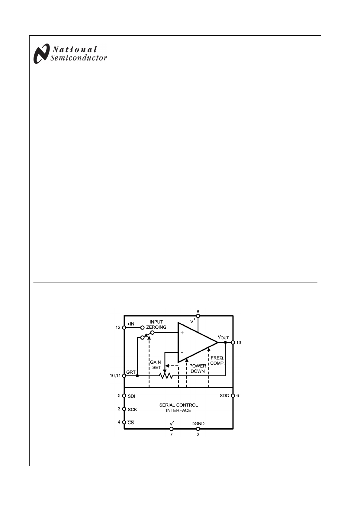
Simplified Block Diagram
20147607
LMP® is a registered trademark of National Semiconductor Corporation.
© 2007 National Semiconductor Corporation 201476 www.national.com
LMP8100 Programmable Gain Amplifier
Page 2
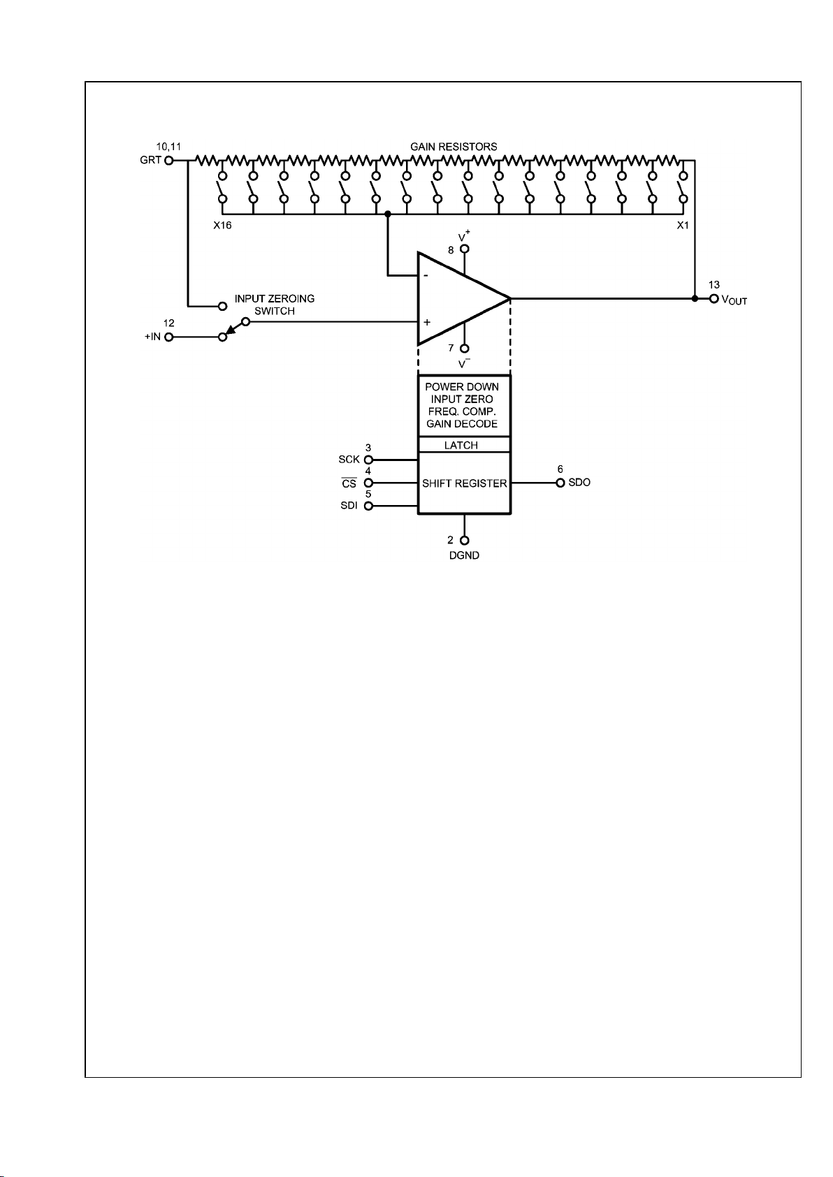
Block Diagram
20147602
www.national.com 2
LMP8100
Page 3
Absolute Maximum Ratings (Note 1)
If Military/Aerospace specified devices are required,
please contact the National Semiconductor Sales Office/
Distributors for availability and specifications.
ESD Tolerance (Note 2)
Human Body Model 2 kV
Machine Model 200V
VIN Differential
2.5V
Output Short Circuit Duration (Note 3)
Supply Voltage (VS = V+ – V−)
6V
Voltage at Input and Output Pins V+ +0.3V, V− −0.3V
Input Current ±10 mA
Storage Temperature Range −65°C to +150°C
Junction Temperature (Note 4) +150°C
Soldering Information
Lead Temperature, Infrared or
Convection Reflow (20 sec) 235°C
Lead Temperature, Wave Solder (10
sec) 260°C
Operating Ratings (Note 1)
Supply Voltage (VS = V+ – V−)
2.7V to 5.5V
Junction Temperature Range (Note 4)
LMP8100A −40°C to +125°C
LMP8100 −40°C to +85°C
Package Thermal Resistance (θJA (Note 4)
14-Pin SOIC 145°C/W
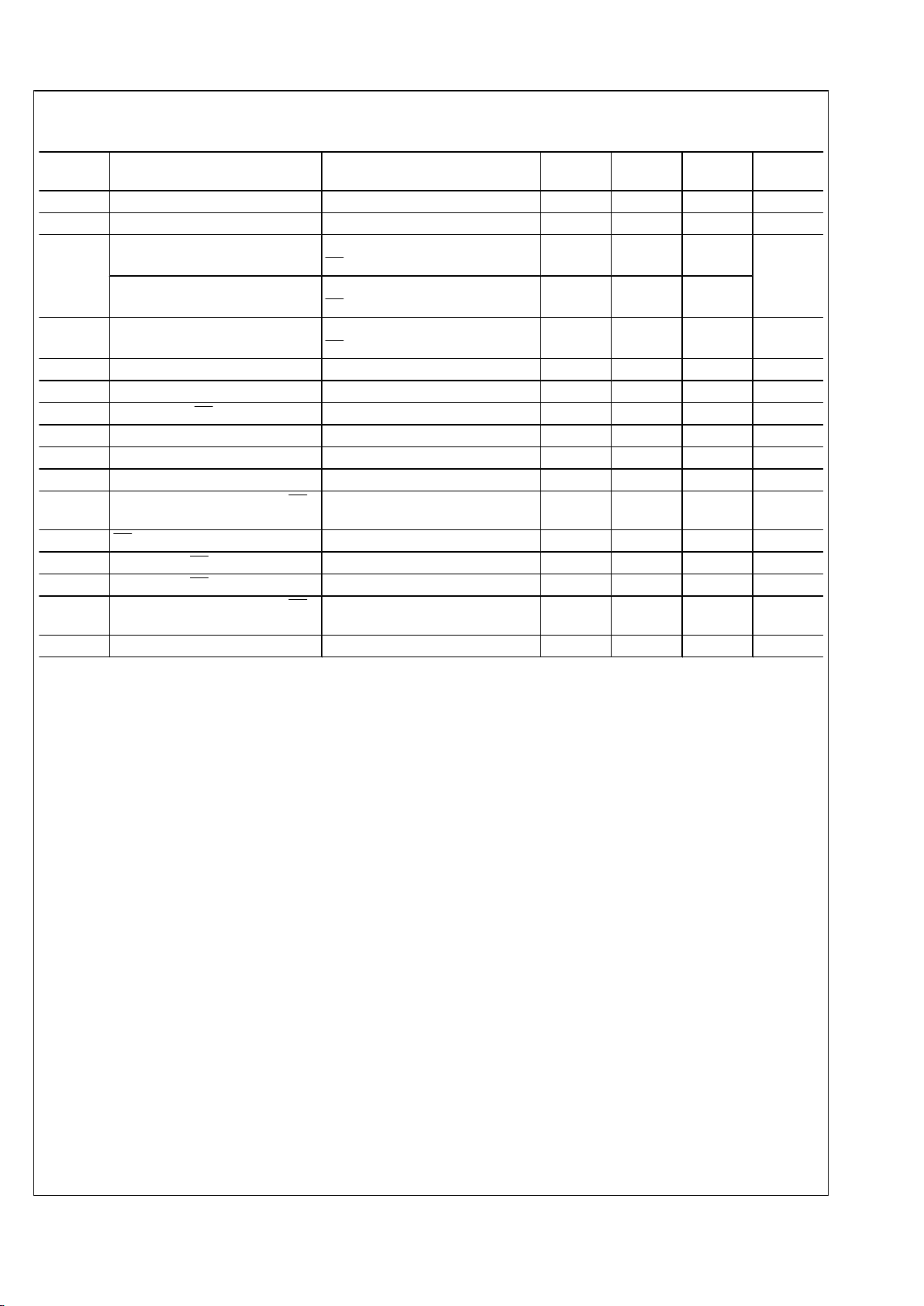
5V Electrical Characteristics
Unless otherwise specified, all limits are guaranteed for TA = 25°C. V+ = 5V , V– = 0V, DGND = 0V, +IN = GRT = V+/2, RL = 10
kΩ to V+/2; Gain = 1 V/V. Boldface limits apply at the temperature extremes.
Symbol Parameter Conditions Min
(Note 6)
Typ
(Note 5)
Max
(Note 6)
Units
Gain Error LMP8100A 0V < +IN (DC) < 3.5V,
1 V/V ≤ Gain ≤ 16 V/V,
0.5V < V
OUT
< 4.5V
0.015 0.03
0.03
%
Gain Error LMP8100 0.015 0.075
0.075
LMP8100 Gain Error (Gain = 1 V/V)
Extended +IN Range
+IN > 3.5V,
0.3V < V
OUT
< 4.7V
0.1
0.2
%
TCGE Gain Drift LMP8100A Gain = 16 0.5 2.2
ppm/°C
LMP8100 Gain = 16 0.8 4.8
V
OS
Input Offset Voltage LMP8100A ±50 ±250
±450
µV
LMP8100 ±50 ±400
±600
TCV
OS
Input Offset Temp Coefficient (Note 8) 1.5 5 µV/°C
I
B
Input Bias Current 0.1 5
100
pA
e
n
Input-Referred Noise Voltage
f = 10 kHz, 1 V/V ≤ Gain ≤ 16 V/V
12
nV/
f = 0.1 Hz to 10 Hz, 1 V/V ≤ Gain
≤ 16 V/V
3.8 µV
PP
BW Bandwidth C1 = C0 = 0, Gain = 1 V/V 33
MHz
C1 = C0 = 0, Gain = 2 V/V 15.5
C1 = C0 = 1, Gain = 16 V/V 9.5
SR Slew Rate (Note 7) 12 V/µs
PSRR Power Supply Rejection Ratio 2.7V < V+ < 5.5V 90
85
100
dB
V
O
Output Swing
High
+IN = 5V 4.9
4.85
4.95
V
Output Swing
Low
+IN = 0V 50 100
150
mV
I
O
Output Current Sourcing and Sinking 15 20 mA
V
IN
Input Voltage Range –0.2
0
5.2
5.0
V
I
S
Supply Current 5.3 6.0
7.2
mA
3 www.national.com
LMP8100
Page 4
Symbol Parameter Conditions Min
(Note 6)
Typ
(Note 5)
Max
(Note 6)
Units
I
PD
Supply Current, Power Down 3.5 20
40
µA
Feedback Resistance 5.6
kΩ
R
IN
Input Impedance f = 10 Hz >10
GΩ
3.3V Electrical Characteristics
Unless otherwise specified, all limits are guaranteed for TA = 25°C. V+ = 3.3V , V– = 0V, DGND = 0V, +IN = GRT = V+/2,
RL = 10 kΩ to V+/2; Gain = 1 V/V. Boldface limits apply at the temperature extremes.
Symbol Parameter Conditions Min
(Note 6)
Typ
(Note 5)
Max
(Note 6)
Units
Gain Error LMP8100A 0V < +IN < 1.8V,
1 V/V ≤ Gain ≤ 16 V/V,
0.3V < V
OUT
< 3.0V
0.015 0.03
0.03
%
Gain Error LMP8100 0.015 0.075
0.075
LMP8100 Gain Error (Gain = 1 V/V)
Extended +IN Range
+IN > 1.8V,
0.3V < V
OUT
< 3.0V
0.1
0.2
%
TCGE Gain Drift LMP8100A Gain = 16 0.5 2.2
ppm/°C
LMP8100 Gain = 16 0.8 4.8
V
OS
Input Offset Voltage LMP8100A ±50 ±250
±450
µV
LMP8100 ±50 ±400
±600
TCV
OS
Input Offset Temp Coefficient (Note 8) 1.5 5 µV/°C
I
B
Input Bias Current 0.1 5
100
pA
e
n
Input-referred Noise Voltage
f = 10 kHz, 1 V/V ≤ Gain ≤ 16 V/V
12
nV/
f = 0.1 Hz to 10 Hz, 1 V/V ≤ Gain ≤
16 V/V
3.8 µV
PP
BW Bandwidth C1 = C0 = 0, Gain = 1 V/V 33
MHzC1 = C0 = 0, Gain = 2 V/V 15.5
C1 = C0 = 1, Gain = 16 V/V 9.5
SR Slew Rate (Note 7) 12 V/µs
PSRR Power Supply Rejection Ratio 2.7V < V+ < 3.6V 90
80
100
dB
V
O
Output Swing
High
+IN = 3.3V 3.2
3.15
3.25
V
Output Swing
Low
+IN = 0V 50 100
150
mV
I
O
Output Current Sourcing and Sinking 15 20 mA
V
IN
Input Voltage Range −0.2
0
3.5
3.3
V
I
S
Supply Current 5.1 5.8
7.0
mA
I
PD
Supply Current, Power Down 1.8 20
40
µA
Feedback Resistance 5.6
kΩ
R
IN
Input Impedance >10
GΩ
www.national.com 4
LMP8100
Page 5
Electrical Characteristics (Serial Interface)
Unless otherwise specified, all limits guaranteed for TA = 25°C, V+ - V− ≥ 2.7V, VD = V+ - DGND ≥ 2.5V.
Symbol Parameter Conditions Min
(Note 6)
Typ
(Note 5)
Max
(Note 6)
Units
V
IL
Logic Low Threshold
0.3 × V
D
V
V
IH
Logic High Threshold
0.7 × V
D
V
I
SDO
Output Source Current, SDO VD = 3.3V or 5.0V,
CS = 0V, VOH = V+ – 0.7V
−7
mA
Output Sink Current, SDO VD = 3.3V or 5.0V,
CS = 0V, VOL = 1.0V
10
I
OZ
Output Tri-state Leakage Current,
SDO
VD = 3.3V or 5.0V,
CS = VD = 3.3V or 5V
±1 µA
t
1
High Period, SCK (Note 9) 100
ns
t
2
Low Period, SCK (Note 9) 100
ns
t
3
Set Up Time, CS to SCK (Note 9) 50
ns
t
4
Set Up Time, SDI to SCK (Note 9) 30
ns
t
5
Hold Time, SCK to SDI (Note 9) 10
ns
t
6
Prop. Delay, SCK to SDO (Note 9)
60 ns
t
7
Hold Time, SCK Transition to CS
Rising Edge
(Note 9) 50
ns
t
8
CS Inactive (Note 9) 50
ns
t
9
Prop. Delay, CS to SDO Active (Note 9)
50 ns
t
10
Prop. Delay, CS to SDO Inactive (Note 9)
50 ns
t
11
Hold Time, SCK Transition to CS
Falling Edge
(Note 9) 10
ns
tR/t
F
Signal Rise and Fall Times (Note 9) 1.5
5 ns
Note 1: Absolute Maximum Ratings indicate limits beyond which damage to the device may occur. Operating Ratings indicate conditions for which the device is
intended to be functional, but for which specific performance is not guaranteed. For guaranteed specifications and the test conditions, see Electrical Characteristics.
Note 2: Human Body Model, applicable std. MIL-STD-883, Method 3015.7. Machine Model, applicable std. JESD22–A115–A (ESD MM std. of JEDEC). FieldInduced Charge-Device Model, applicable std. JESD22–C101–C (ESD FICDM std. of JEDEC).
Note 3: The short circuit test is a momentary test which applies to both single-supply and split-supply operation. Continuous short circuit operation at elevated
ambient temperature can exceed the maximum allowable junction temperature of 150°C.
Note 4: The maximum power dissipation is a function of T
J(MAX)
, θJA. The maximum allowable power dissipation at any ambient temperature is PD = (T
J(MAX)
–
TA)/ θJA. All numbers apply for packages soldered directly onto a PC Board.
Note 5: Typical Values indicate the most likely parametric norm as determined at the time of characterization. Actual typical values may vary over time and will
also depend on the application and configuration. The typical values are not tested and are not guaranteed on shipped production material.
Note 6: All limits are guaranteed by testing or statistical analysis.
Note 7: Slew rate is the average of the rising and falling slew rates.
Note 8: The offset voltage average drift is determined by dividing the value of VOS at the temperature extremes by the total temperature change.
Note 9: Load for these tests is shown in the Timing Diagram Test Circuit.
5 www.national.com
LMP8100
Page 6
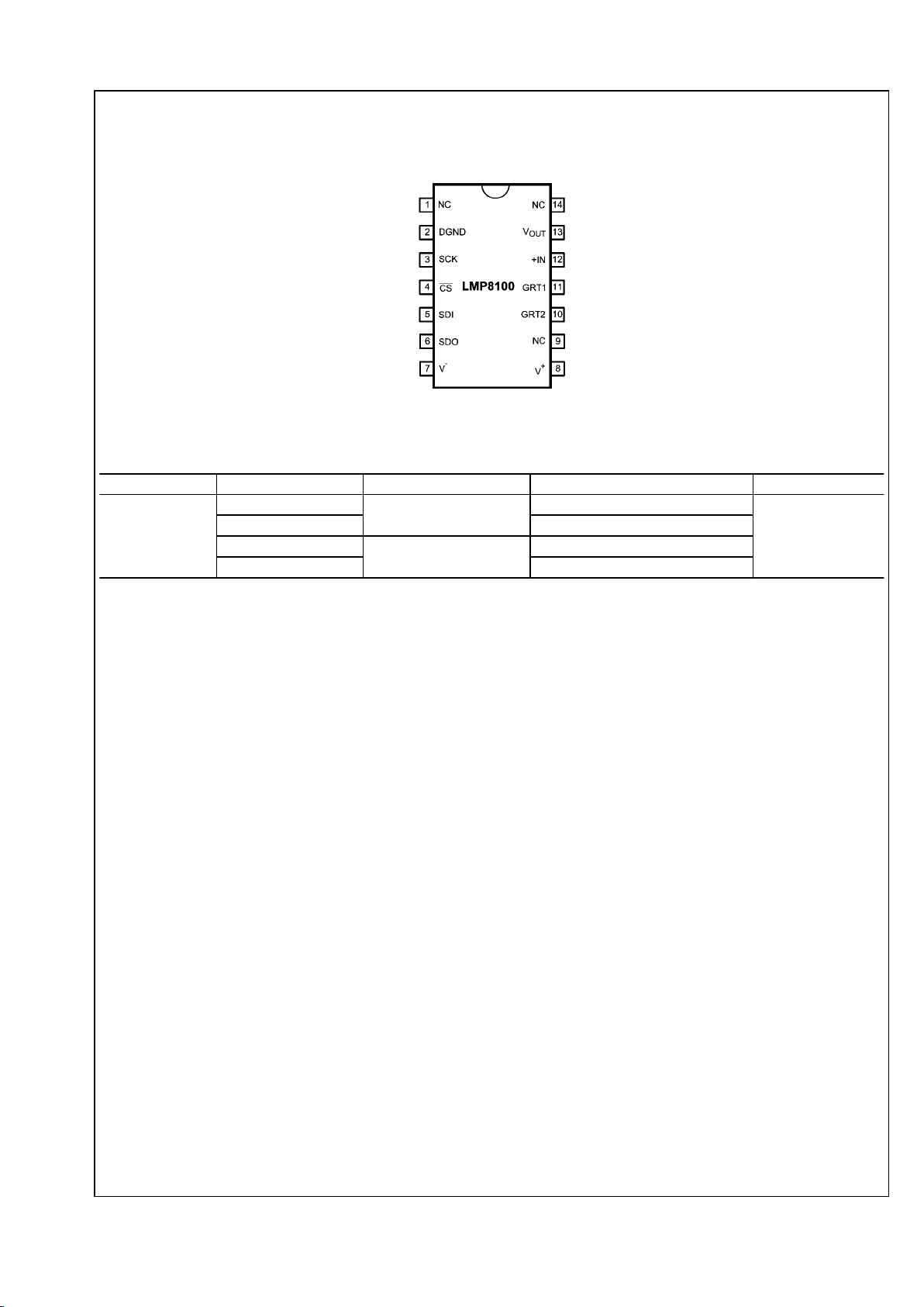
Connection Diagram
14-Pin SOIC
20147601
Top View
Ordering Information
Package Part Number Package Marking Transport Media NSC Drawing
14-Pin SOIC
LMP8100AMA
LMP8100AMA
55 Units/Rail
M14A
LMP8100AMAX 2.5k units Tape and Reel
LMP8100MA
LMP8100MA
55 Units/Rail
LMP8100MAX 2.5k units Tape and Reel
www.national.com 6
LMP8100
Page 7
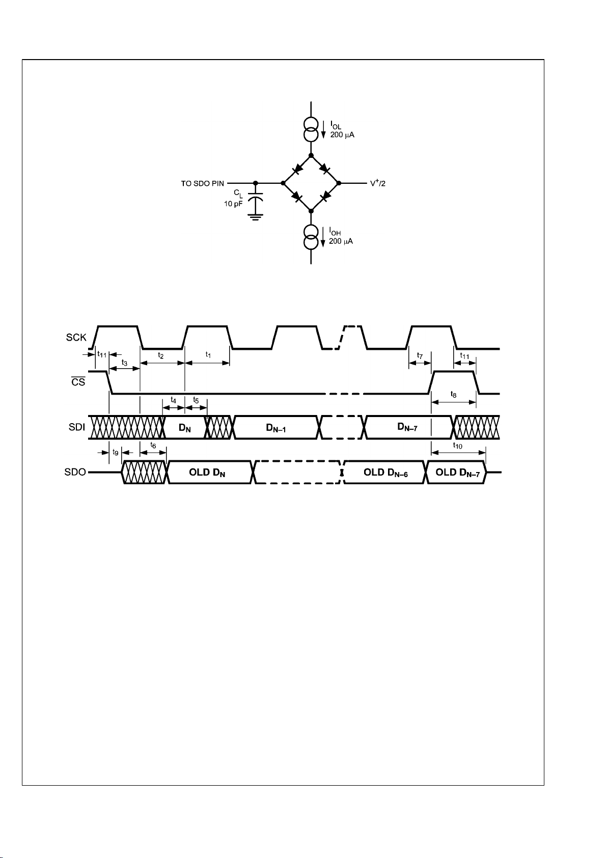
Timing Diagram Test Circuit
20147653
Timing Diagram
20147603
7 www.national.com
LMP8100
Page 8
Test Circuit Diagram
20147609
Test Circuit
www.national.com 8
LMP8100
Page 9
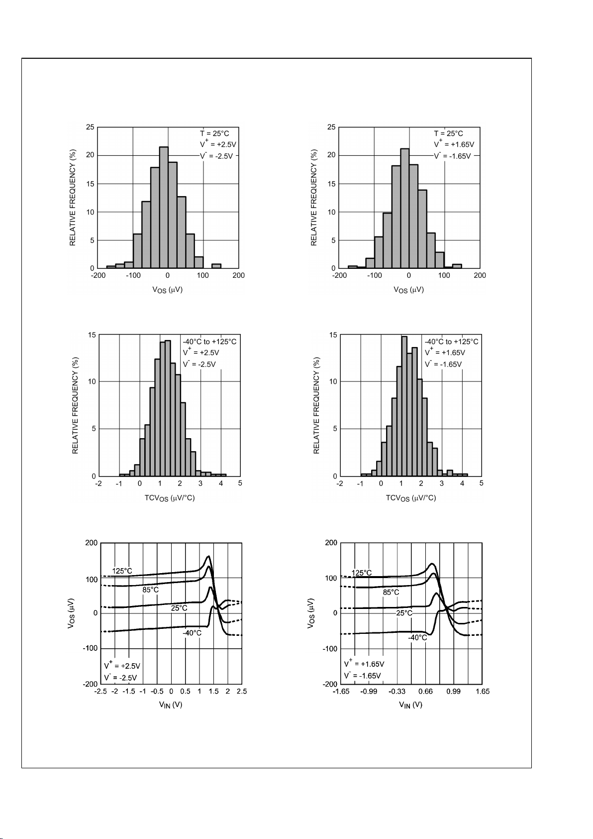
Typical Performance Characteristics
Offset Voltage Distribution
20147685
Offset Voltage Distribution
20147686
TCVOS Distribution
20147683
TCVOS Distribution
20147684
VOS vs. V
IN
20147666
VOS vs. V
IN
20147667
9 www.national.com
LMP8100
Page 10

VOS vs. V
S
20147665
VOS vs. V
S
20147664
IB vs. V
IN
20147662
IB vs. V
IN
20147663
IS vs. V
S
20147660
IS vs. V
S
20147661
www.national.com 10
LMP8100
Page 11

DC Gain Error A = 1
20147689
DC Gain Error A = 1
20147687
DC Gain Error A = 2
20147690
DC Gain Error A = 2
20147688
Small Signal Gain Error vs. +IN DC Level
20147633
Small Signal Gain Error vs. +IN DC Level
20147651
11 www.national.com
LMP8100
Page 12

PSRR vs. Frequency
20147610
PSRR vs. Frequency
20147611
I
OUT
vs. V
OUT
(Source)
20147669
I
OUT
vs. V
OUT
(Sink)
20147668
I
OUT
vs. V
OUT
(Source)
20147671
I
OUT
vs. V
OUT
(Sink)
20147670
www.national.com 12
LMP8100
Page 13

Small Signal Step Response
20147635
Small Signal Step Response
20147636
Small Signal Step Response
20147637
Small Signal Step Response
20147638
Small Signal Step Response
20147639
Small Signal Step Response
20147640
13 www.national.com
LMP8100
Page 14

Small Signal Step Response
20147641
Small Signal Step Response
20147642
Large Signal Step Response
20147643
Large Signal Step Response
20147644
Large Signal Step Response
20147645
Large Signal Step Response
20147646
www.national.com 14
LMP8100
Page 15

Large Signal Step Response
20147647
Large Signal Step Response
20147648
Large Signal Step Response
20147649
Large Signal Step Response
20147650
THD+N vs. Frequency
20147675
THD+N vs. Frequency
20147674
15 www.national.com
LMP8100
Page 16

THD+N vs. V
OUT
20147673
THD+N vs. V
OUT
20147672
Bandwidth vs. Capacitive Load
20147617
Bandwidth vs. Capacitive Load
20147618
Peaking vs. Capacitive Load
20147621
Peaking vs. Capacitive Load
20147622
www.national.com 16
LMP8100
Page 17

Peaking vs. Capacitive Load
20147623
Gain vs. Frequency
20147630
Gain vs. Frequency
20147629
Gain vs. Frequency
20147628
Gain vs. Frequency
20147627
AC Gain Error vs. Frequency
20147656
17 www.national.com
LMP8100
Page 18

AC Gain Error vs. Frequency
20147655
AC Gain Error vs. Frequency
20147657
AC Gain Error vs. Frequency
20147658
AC Gain Error vs. Frequency
20147659
Noise vs. Frequency
20147654
0.1 Hz to 10 Hz Noise
201476a2
www.national.com 18
LMP8100
Page 19

Closed Loop Output Impedance vs. Frequency
20147631
Input Impedance
201476a1
SDO V vs. I
20147634
SDO V vs. I
20147652
19 www.national.com
LMP8100
Page 20

Applications Information
LIFETIME DRIFT
Offset voltage (VOS) and gain are electrical parameters which
may drift over time. This drift, known as lifetime drift, is very
common in operational amplifiers; however, its effect is more
evident in precision amplifiers. This is due to the very low offset voltage specification and very precise gain specification
of the LMP8100. The LMP8100 has an option to zero out the
offset voltage. When the zero bit of the register is set high,
+IN is connected to GRT. Output offset voltage can be measured and adjusted out of the signal path. See the “Input
Zeroing” section, for more information. Numerous reliability
tests have been performed to characterize this drift for the
LMP8100. Prior to each long term reliability test the input offset voltage and gain at 2X and 16X of each LMP8100 was
measured at room temperature.
The long term reliability tests include Operating Life Time
(OPL) performed at 150°C for an extended period of time and
Temperature Humidity Bias Testing (THBT) at 85°C and 85%
humidity for an extended period of time. The offset voltage
and gain of 2X and 16X were measured again at room temperature after each reliability test.
The offset voltage drift is the difference between the initial
measurement and the later measurement, after the reliability
test.
The gain drift is the percentage difference between the initial
measurement and the later measurement, after the reliability
test. Figure 1 – Figure 4 show the offset voltage drift and gain
drift after 1000 hours of OPL.
Figure 5 – Figure 8 show the offset voltage drift and gain drift
after 1000 hours of THBT.
20147691
FIGURE 1. OPL VOS Drift
20147692
FIGURE 2. OPL VOS Drift
20147693
FIGURE 3. OPL Gain Drift, A = 2
20147694
FIGURE 4. OPL Gain Drift, A = 16
www.national.com 20
LMP8100
Page 21

20147695
FIGURE 5. THBT VOS Drift
20147696
FIGURE 6. THBT VOS Drift
20147697
FIGURE 7. THBT Gain Drift, A = 2
20147698
FIGURE 8. THBT Gain Drift, A = 16
POWER-ON RESET
The LMP8100 has a power-up reset feature that sets all the
register bits to 0 when the part is powered up. To implement
this feature the CS
and SCK pins must be held at or above
VIH when the LMP8100 is powered-up. Failure to power up in
this method can lead to an unpredictable state of the register
bits after power-up.
CONTROL REGISTER
The control register retains the information which controls the
amplifier gain, bandwidth compensation, input zeroing, and
power down. The register is loaded by way of the serial control
interface. The register is double buffered so that changes can
be made with minimum effect on amplifier performance. Table
1 shows the organization of the control register. Table 2 gives
the codes for gain setting, input zeroing and power down control. Table 3 shows the codes for the four gain-bandwidth
compensation levels.
TABLE 1. Control Register Format
C1 C0 Zero PD G3 G2 G1 G0
MSB LSB
C0, C1: Compensation setting
Zero: Zero Input
PD: Power Down
G0 to G3: Gain setting
21 www.national.com
LMP8100
Page 22

TABLE 2. Input Zero, Power-Down
and Gain Setting Codes
Zero PD G3 G2 G1 G0 Non-Inverting
Gain
0 0 0 0 0 1
0 0 0 0 1 2
0 0 0 1 0 3
0 0 0 1 1 4
0 0 1 0 0 5
0 0 1 0 1 6
0 0 1 1 0 7
0 0 1 1 1 8
0 1 0 0 0 9
0 1 0 0 1 10
0 1 0 1 0 11
0 1 0 1 1 12
0 1 1 0 0 13
0 1 1 0 1 14
0 1 1 1 0 15
0 1 1 1 1 16
X 1 X X X X Power Down
1 0 X X X X Zero Input
TABLE 3. Amplifier Gain Compensation Codes
C1 C0 Compensation
Level
Condition
0 0 0
Maximum
Compensation
0 1 1
1 0 2
1 1 3
Minimum
Compensation
AMPLIFIER GAIN SETTING AND BANDWIDTH
COMPENSATION CONTROL
The gain of the LMP8100 is set to one of 16 levels under program control by setting the appropriate bits G[3:0] of the
control register with a number from 00h to 15h. This sets the
gain to a level from 1 V/V to 16 V/V respectively.
The gain-bandwidth compensation is also selectable to one
of four levels under program control. The amount of compensation can be decreased to maximize the available bandwidth
as the gain of the amplifier is increased. The compensation
level is selected by setting bits C[1:0] of the control register
with a number from 00b to 11b with 00b being maximum compensation and 11b being minimum compensation. Table 4
shows the bandwidths achieved at several gain and compensation settings. It will be noted that for gains between X1 and
X5, the recommended compensation setting is 00b. For gain
settings between X6 and X10, compensation settings may be
00b and 01b. Gain settings between X11 and X15 may use
the three bandwidth compensation settings between 00b and
10b. At a gain of X16, all bandwidth compensation ranges
may be used. Note that, for lower gains, it is possible to undercompensate the amplifier into instability.
TABLE 4. Amplifier Gain and Compensation
vs. Bandwidth
Gain Compensation Bits 3 dB Bandwidth
(MHz)
V/V dB C1 C0
1 0 0 0 33.0
2 6.02 0 0 15.5
6 15.6 0 0 4.2
6 15.6 0 1 8.3
11 20.8 0 0 2.0
11 20.8 0 1 3.9
11 20.8 1 0 6.6
16 24.1 0 0 1.3
16 24.1 0 1 2.3
16 24.1 1 0 3.8
16 24.1 1 1 9.5
NON-INVERTING AMPLIFIER OPERATION
The principal application of the LMP8100 is as a non-inverting
amplifier as shown in the simplified schematic, Figure 9. The
amplifier supply voltage (V+ to V−) is specified as 5.5V maximum. The V– supply pin is connected to the system ground
for single supply operation. V− can be returned to a negative
voltage when required by the application. The digital supply
voltage for the serial interface is applied between the V+ supply pin and DGND.
20147605
FIGURE 9. Basic Non-Inverting Amplifier
www.national.com 22
LMP8100
Page 23

GRT PINS
The GRT pins must have a low impedance connection to either ground or a reference voltage. Any parasitical impedance
on these pins will affect the gain accuracy of the LMP8100.
Figure 10 shows a simplified schematic of the LMP8100
showing the internal gain resistors and an external parasitical
resistance RP. The gain of the LMP8100 is determined by
RF and RG, the values of which are set by the internal register.
The gain of the amplifier is given by the equation
Any resistance between the GRT pins and either ground or a
reference voltage will change the gain to
20147679
FIGURE 10. LMP8100 with External Parasitical
Resistance
The connection between the GRT pins and ground or a reference voltage should be as short as possible using wide
traces to minimize the parasitical resistance. Figure 11 shows
two suggested methods of connecting the GRT pins to a
ground plane on the same layer or to a ground plane on a
different layer of the PCB.
20147676
FIGURE 11. GRT Connection Methods
The GRT pin can be connected to a reference voltage source
to provide an offset adjustment to the gain function. Any DC
resistance that may be present between the voltage source
and the GRT pin must be kept to an absolute minimum to
avoid introducing gain errors into the circuit.
INPUT ZEROING
Measurements made with the LMP8100 in the signal path
may be adjusted for the output offset voltage of the amplifier.
For example: The measurement of V
OUT
for offset correction
might be made using an ADC under microprocessor control.
Output offset is measured under program control by setting
the ZERO bit in the programming register. In this mode, +IN
is disconnected from the input pin and internally connected to
the GRT input. Figure 12 shows the LMP8100 in the input
zeroing mode.
23 www.national.com
LMP8100
Page 24

20147606
FIGURE 12. Non-Inverting Input Zeroing Function
SERIAL CONTROL INTERFACE OPERATION
The LMP8100 gain, bandwidth compensation, power down,
and input zeroing are controlled by data stored in a programming register. Data to be written into the control register is first
loaded into the LMP8100 via the serial interface. The serial
interface employs an 8-bit shift register. Data is loaded
through the serial data input, SDI. Data passing through the
shift register is output through the serial data output, SDO.
The serial clock, SCK controls the serial loading process. All
eight data bits are required to correctly program the amplifier.
The falling edge of CS enables the shift register to receive
data. The SCK signal must be high during the falling and rising
edge of CS. Each data bit is clocked into the shift register on
the rising edge of SCK. Data is transferred from the shift register to the holding register on the rising edge of CS. Operation
is shown in the timing diagram,Figure 13.
20147624
FIGURE 13. Serial Control Interface Timing
www.national.com 24
LMP8100
Page 25

The serial control pins can be connected in one of two ways
when two or more LMP8100s are used in an application.
Star Configuration
This configuration can be used if each LMP8100 will always
have the same value in each register. The connections are
shown in Figure 14. After the microcontroller writes a byte all
registers will have the same value.
20147680
FIGURE 14. Star Configuration
Daisy Chain Configuration
This configuration can be used to program the same or different values in the register of each LMP8100. The connections are shown in Figure 15. In this configuration the SDO
pin of each LMP8100 is connected to the SDI pin of the fol-
lowing LMP8100. The following two examples show how the
registers are written.
If all three LMP8100s need a gain of 11 with a compensation level of 10. (10001010)
Register of
LMP8100 #1
Register of
LMP8100 #2
Register of
LMP8100 #3
Notes
Power on 00000000 00000000 00000000 Default power on state (see above)
Byte one sent 10001010 00000000 00000000 The data in the register of LMP8100 #1 is
shifted into the register of LMP8100 #2, the
data in the register of LMP8100 #2 is shifted
into the register of LMP8100 #3.
Byte two sent 10001010 10001010 00000000
Byte three sent 10001010 10001010 10001010
If LMP8100 #1 needs a gain of 11 with a compensation level of 10 (10001010), LMP8100 #2 needs a gain of 6 with a compensation
of 00 (00000101), and LMP8100 #3 needs a gain of 2 with a compensation of 00 (00000001).
Register of
LMP8100 #1
Register of
LMP8100 #2
Register of
LMP8100 #3
Notes
Power on 00000000 00000000 00000000 Default power on state (see above)
Byte one sent 00000001 00000000 00000000 The data in the register of LMP8100 #1 is
shifted into the register of LMP8100 #2, the
data in the register of LMP8100 #2 is shifted
into the register of LMP8100 #3.
Byte two sent 00000101 00000001 00000000
Byte three sent 10001010 00000101 00000001
25 www.national.com
LMP8100
Page 26

20147681
FIGURE 15. Daisy Chain Configuration
POWER SUPPLY PURITY AND BYPASSING
Particular attention to power supply purity is needed in order
to preserve the LMP8100's gain accuracy and low noise. The
LMP8100 worst-case PSRR is 85 dB or 56.2 µV/V. Nevertheless, the usable dynamic range, gain accuracy and inherent low noise of the amplifier can be compromised through
the introduction and amplification of power supply noise.
To decouple the LMP8100 from supply line AC noise, a 0.1
µF capacitor should be located on each supply line, close to
the LMP8100. Adding a 10 µF capacitor in parallel with the
0.1 µF capacitor will reduce the noise introduced to the
LMP8100 even more by providing an AC path to ground for
most frequency ranges.
A power supply dropout (V+ -V− < 2.7V) can cause an unintended reset of the register. If a dropout occurs, the register
will need to be reprogrammed with the correct values.
SCALING AMPLIFIER
The LMP8100 is ideally suited for use as an amplifier between
a sensor that has a wide output range and an ADC. As the
signal from the sensor changes the gain of the LMP8100 can
be changed so that the entire input range of the ADC is being
used at all times. Figure 16 shows a data acquisition system
using the LMP8100 and the ADC121S101. The 100Ω resistor
and 390 pF capacitor form an antialiasing filter for the ADC121S101. The capacitor also stores and delivers charge to
the switched capacitor input of the ADC. The capacitive load
on the LMP8100 created by the 390pF capacitor is decreased
by the 100Ω resistor.
20147682
FIGURE 16. Data Acquisition System Using the LMP8100
www.national.com 26
LMP8100
Page 27

BRIDGE AMPLIFIER
In Figure 17 two LMP8100s are used with a LMP7711 to build
an amplifier for the signal from a GMR Magnetic Field Sensor.
The advantage of using the LMP8100 is that as the signal
strength from the Magnetic Field Sensor decreases, the gain
of the LMP8100 can be increased. An example is if the signal
from this composite amplifier is used to drive an ADC. When
the maximum magnetic field to be measured is applied, the
gain of the LMP7711 can be set to supply a full range signal
to the ADC input with the gain of the LMP8100 set to one. As
the magnetic field decreases, the gain of the LMP8100 can
be increased, so that the signal supplied to the ADC uses a
maximum amount of the ADC input range.
The following can be done to maximize performance:
•
Connect the GRT pins directly together and to GND with
a low impedance trace.
•
Make the traces between the Magnetic Field Sensor and
the LMP8100s short to minimize noise pickup.
•
Place 0.1 μF capacitors close to each of the LMP8100
supply pins.
The following can be done to simplify the design:
•
Connect the SCL, SCK, and CS lines in parallel and one
microcontroller can be used to drive both LMP8100s.
•
The SDO pin can be left floating.
The LM317 and LM6171 are used for the supply of the Magnetic Sensor. The 100Ω potentiometer is used to adjust the
supply voltage to the Magnetic Field Sensor. The 2 kΩ potentiometer is used to fine tune the negative supply to set the
Magnetic Field Sensor output to zero.
20147625
FIGURE 17. Bridge Amplifier
27 www.national.com
LMP8100
Page 28

Physical Dimensions inches (millimeters) unless otherwise noted
14-Pin SOIC
NS Package Number M14A
www.national.com 28
LMP8100
Page 29

Notes
29 www.national.com
LMP8100
Page 30

Notes
LMP8100 Programmable Gain Amplifier
THE CONTENTS OF THIS DOCUMENT ARE PROVIDED IN CONNECTION WITH NATIONAL SEMICONDUCTOR CORPORATION
(“NATIONAL”) PRODUCTS. NATIONAL MAKES NO REPRESENTATIONS OR WARRANTIES WITH RESPECT TO THE ACCURACY
OR COMPLETENESS OF THE CONTENTS OF THIS PUBLICATION AND RESERVES THE RIGHT TO MAKE CHANGES TO
SPECIFICATIONS AND PRODUCT DESCRIPTIONS AT ANY TIME WITHOUT NOTICE. NO LICENSE, WHETHER EXPRESS,
IMPLIED, ARISING BY ESTOPPEL OR OTHERWISE, TO ANY INTELLECTUAL PROPERTY RIGHTS IS GRANTED BY THIS
DOCUMENT.
TESTING AND OTHER QUALITY CONTROLS ARE USED TO THE EXTENT NATIONAL DEEMS NECESSARY TO SUPPORT
NATIONAL’S PRODUCT WARRANTY. EXCEPT WHERE MANDATED BY GOVERNMENT REQUIREMENTS, TESTING OF ALL
PARAMETERS OF EACH PRODUCT IS NOT NECESSARILY PERFORMED. NATIONAL ASSUMES NO LIABILITY FOR
APPLICATIONS ASSISTANCE OR BUYER PRODUCT DESIGN. BUYERS ARE RESPONSIBLE FOR THEIR PRODUCTS AND
APPLICATIONS USING NATIONAL COMPONENTS. PRIOR TO USING OR DISTRIBUTING ANY PRODUCTS THAT INCLUDE
NATIONAL COMPONENTS, BUYERS SHOULD PROVIDE ADEQUATE DESIGN, TESTING AND OPERATING SAFEGUARDS.
EXCEPT AS PROVIDED IN NATIONAL’S TERMS AND CONDITIONS OF SALE FOR SUCH PRODUCTS, NATIONAL ASSUMES NO
LIABILITY WHATSOEVER, AND NATIONAL DISCLAIMS ANY EXPRESS OR IMPLIED WARRANTY RELATING TO THE SALE
AND/OR USE OF NATIONAL PRODUCTS INCLUDING LIABILITY OR WARRANTIES RELATING TO FITNESS FOR A PARTICULAR
PURPOSE, MERCHANTABILITY, OR INFRINGEMENT OF ANY PATENT, COPYRIGHT OR OTHER INTELLECTUAL PROPERTY
RIGHT.
LIFE SUPPORT POLICY
NATIONAL’S PRODUCTS ARE NOT AUTHORIZED FOR USE AS CRITICAL COMPONENTS IN LIFE SUPPORT DEVICES OR
SYSTEMS WITHOUT THE EXPRESS PRIOR WRITTEN APPROVAL OF THE CHIEF EXECUTIVE OFFICER AND GENERAL
COUNSEL OF NATIONAL SEMICONDUCTOR CORPORATION. As used herein:
Life support devices or systems are devices which (a) are intended for surgical implant into the body, or (b) support or sustain life and
whose failure to perform when properly used in accordance with instructions for use provided in the labeling can be reasonably expected
to result in a significant injury to the user. A critical component is any component in a life support device or system whose failure to perform
can be reasonably expected to cause the failure of the life support device or system or to affect its safety or effectiveness.
National Semiconductor and the National Semiconductor logo are registered trademarks of National Semiconductor Corporation. All other
brand or product names may be trademarks or registered trademarks of their respective holders.
Copyright© 2007 National Semiconductor Corporation
For the most current product information visit us at www.national.com
National Semiconductor
Americas Customer
Support Center
Email:
new.feedback@nsc.com
Tel: 1-800-272-9959
National Semiconductor Europe
Customer Support Center
Fax: +49 (0) 180-530-85-86
Email: europe.support@nsc.com
Deutsch Tel: +49 (0) 69 9508 6208
English Tel: +49 (0) 870 24 0 2171
Français Tel: +33 (0) 1 41 91 8790
National Semiconductor Asia
Pacific Customer Support Center
Email: ap.support@nsc.com
National Semiconductor Japan
Customer Support Center
Fax: 81-3-5639-7507
Email: jpn.feedback@nsc.com
Tel: 81-3-5639-7560
www.national.com
 Loading...