

Page 1
September 2007
LMP7300
Micropower Precision Comparator and Precision
Reference with Adjustable Hysteresis
General Description
The LMP7300 is a combination comparator and reference
with ideal specifications for precision threshold detecting. The
precision 2.048V reference comes with a 0.25% maximum
error. The comparator features micopower (35 µW), low offset
voltage (.75 mV max), and independent adjustable positive
and negative hysteresis.
Hysteresis control for the comparator is accomplished
through two external pins. The HYSTP pin sets the positive
hysteresis and the HYSTN pin sets the negative hysteresis.
The comparator design isolates the VIN source impedance
and the programmable hysteresis components. This isolation
prevents any undesirable interaction allowing the IC to maintain a precise threshold voltage during level detection.
The combination of low offset voltage, external hysteresis
control, and precision voltage reference provides an easy to
use micropower precision threshold detector.
The LMP7300 open collector output makes it ideal for mixed
voltage system designs. The output voltage upper rail is unconstrained by VCC and can be pulled above VCC to a maximum of 12V. The LMP7300 is a member of the LMP
®
precision amplifier family.
Features
(For VS = 5V, typical unless otherwise noted)
■
Supply current
13 μA
■
Propagation delay
4 μs
■
Input offset voltage 0.3 mV
■
CMRR 100 dB
■
PSRR 100 dB
■
Positive and negative hysteresis control
■
Adjustable hysteresis 1 mV/mV
■
Reference voltage 2.048V
■
Reference voltage accuracy 0.25%
■
Reference voltage source current 1 mA
■
Wide supply voltage range 2.7V to 12V
■
Operating temperature range ambient −40°C to 125°C
Applications
■
Precision threshold detection
■
Battery monitoring
■
Battery management systems
■
Zero crossing detectors
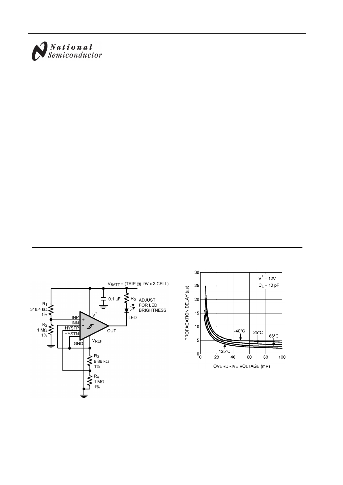
Typical Application
Micropower Precision Battery Low Voltage Detector for 3
Cell Discharge Voltage
20175646
20175642
LMP® is a registered trademark of National Semiconductor Corporation.
© 2007 National Semiconductor Corporation 201756 www.national.com
LMP7300 Micropower Precision Comparator and Precision Reference with Adjustable
Hysteresis
Page 2
Absolute Maximum Ratings (Note 1)
If Military/Aerospace specified devices are required,
please contact the National Semiconductor Sales Office/
Distributors for availability and specifications.
ESD Tolerance (Note 2)
Human Body Model 2000V
Machine Model 200V
V
IN
Differential ±V
S
Supply Voltage (VS = V+ – V−)
13.6V
Voltage at Input/Output Pins V+ + 0.3V, V− − 0.3V
Storage Temperature Range −65°C to +150°C
Junction Temperature (Note 3) +150°C
Soldering Information
Infrared or Convection (20 sec) 235°C
Wave Soldering Lead Temp. (10 sec) 260°C
Operating Ratings (Note 1)
Temperature Range (Note 3) −40°C to 125°C
Supply Voltage (VS = V+ – V−)
2.7V to 12V
Package Thermal Resistance (θJA (Note 3))
8-Pin SOIC 166°C/W
8-Pin MSOP 235°C/W
2.7V Electrical Characteristics (Note 4)
Unless otherwise specified, all limits are guaranteed for TA = 25°C, V+ = 2.7V, V− = 0V, and VCM = V+/2, R
PULLUP
= 100 kΩ,
C
LOAD
= 10 pF. Boldface limits apply at the temperature extremes.
Symbol Parameter Conditions Min
(Note 6)
Typ
(Note 5)
Max
(Note 6)
Units
I
S
Supply Current R
PULLUP
= Open 9 12
17
μA
Comparator
V
OS
Input Offset Voltage VCM = V+/2 ±0.07 ±0.75
±2
mV
TCV
OS
Input Offset Average Drift (Note 8) 1.8
μV/°C
I
B
Input Bias Current (Note 7) |VID| < 2.5V
1.2 3
4
nA
I
OS
Input Offset Current 0.15 0.5 nA
CMRR Common Mode Rejection Ratio 1V < V
CM
< 2.7V 80 100
dB
PSRR Power Supply Rejection Ratio V+ = 2.7V to 12V 80 100 dB
V
OL
Output Low Voltage I
LOAD
= 10 mA 0.25 0.4
0.5
V
I
LEAK
Output Leakage Current Comparator Output in High State 1 pA
HC
LIN
Hysteresis Control Voltage
Linearity
0 < Ref-HYSTP,N < 25 mV 1.000
mV/V
25 mV < Ref-HYSTP,N < 100 mV 0.950
I
HYS
Hysteresis Leakage Current 1.2 3
4
nA
T
PD
Propagation Delay
(High to Low)
Overdrive = 10 mV, CL = 10 pF 12 17
μs
Overdrive = 100 mV, CL = 10 pF 4.5 7.6
Reference
V
O
Reference Voltage 2.043 2.048 2.053 V
Line Regulation VCC = 2.7V to 12V 14 80
μV/V
Load Regulation I
OUT
= 0 to 1 mA 0.2 0.5
mV/mA
TCV
REF/°C
Temperature Coefficient −40°C to 125°C 55 ppm/°C
V
N
Output Noise Voltage 0.1 Hz to 10 Hz 80
μV
PP
10 Hz to 10 kHz 100
μV
RMS
www.national.com 2
LMP7300
Page 3
5V Electrical Characteristics (Note 4)
Unless otherwise specified, all limits are guaranteed for TA = 25°C, V+ = 5V, V− = 0V, and VCM = V+/2, R
PULLUP
= 100 kΩ, C
LOAD
=
10 pF. Boldface limits apply at the temperature extremes.
Symbol Parameter Conditions Min
(Note 6)
Typ
(Note 5)
Max
(Note 6)
Units
I
S
Supply Current R
PULLUP
= Open 10 13
18
μA
Comparator
V
OS
Input Offset Voltage VCM = V+/2 ±0.07 ±0.75
±2
mV
TCV
OS
Input Offset Average Drift (Note 8) 1.8
μV/°C
I
B
Input Bias Current (Note 7) |VID| < 2.5V 1.2 3
4
nA
I
OS
Input Offset Current 0.15 0.5 nA
CMRR Common Mode Rejection Ratio
1 ≤ VCM ≤ 5V
80 100
dB
PSRR Power Supply Rejection Ratio V+ = 2.7V to 12V 80 100 dB
V
OL
Output Voltage Low I
LOAD
= 10 mA 0.25 0.4 V
I
LEAK
Output Leakage Current Comparator Output in High State 1 pA
HC
LIN
Hysteresis Control Voltage
Linearity
0 < Ref-V
HYS
TP,N < 25 mV 1.000
mV/V
25 mV < Ref-V
HYS
TP,N < 100 mV 0.950
I
HYS
Hysteresis Leakage Current 1.2 3
4
nA
TPD Propagation Delay
(High to Low)
Overdrive = 10 mV, CL = 10 pF 12 15
μs
Overdrive = 100 mV, CL = 10 pF 4 7
Reference
V
O
Reference Voltage 2.043 2.048 2.053 V
Line Regulation VCC = 2.7V to 12V 14 80
μV/V
Load Regulation I
OUT
= 0 to 1 mA 0.2 0.5
mV/mA
TCV
REF/°C
Temperature Coefficient −40°C to 125°C 55 ppm/°C
V
N
Output Noise Voltage 0.1 Hz to 10 Hz 80
μV
PP
10 Hz to 10 kHz 100
μV
RMS
12V Electrical Characteristics (Note 4)
Unless otherwise specified, all limits are guaranteed for TA = 25°C, V+ = 12V, V− = 0V, and VCM = V+/2, R
PULLUP
= 100 kΩ,
C
LOAD
= 10 pF. Boldface limits apply at the temperature extremes.
Symbol Parameter Conditions Min
(Note 6)
Typ
(Note 5)
Max
(Note 6)
Units
I
S
Supply Current R
PULLUP
= Open 11 14
20
µA
Comparator
V
OS
Input Offset Voltage VCM = V+/2 ±0.08 ±0.75
±2
mV
TCV
OS
Input Offset Average Drift (Note 8) 1.8
μV/°C
I
B
Input Bias Current (Note 7) |VID| > 2.5V 1.2 3
4
nA
I
OS
Input Offset Current 0.15 0.5 nA
CMRR Common Mode Rejection Ratio
1V ≤ V
CM
≤ 12V
80 100
dB
PSRR Power Supply Rejection Ratio V+ = 2.7V to 12V 80 100 dB
V
OL
Output Voltage Low I
LOAD
= 10 mA 0.25 0.4 V
I
LEAK
Output Leakage Current Comparator Output in High State 1 pA
3 www.national.com
LMP7300
Page 4
Symbol Parameter Conditions Min
(Note 6)
Typ
(Note 5)
Max
(Note 6)
Units
HC
LIN
Hysteresis Control Voltage
Linearity
0 < Ref-V
+HYS
TP,N < 25 mV 1.000
mV/V
25 mV < Ref-V
+HYS
TP,N < 100 mV 0.950
I
HYS
Hysteresis Leakage Current 1.2 3
4
nA
TPD Propagation Delay
(High to Low)
Overdrive = 10 mV, CL = 10 pF 11 15
μs
Overdrive = 100 mV, CL = 10 pF 3.5 6.8
Reference
V
O
Reference Voltage TJ = 25°C 2.043 2.048 2.053 V
Line Regulation VCC = 2.7V to 12V 14 80
μV/V
Load Regulation I
OUT
= 0 to 1 mA 0.2 0.5 mV/mA
TCV
REF/°C
Temperature Coefficient −40°C to +125°C 55 ppm/°C
V
N
Output Noise Voltage 0.1 Hz to 10 Hz 80
μV
PP
10 Hz to 10 kHz 100
μV
RMS
Note 1: Absolute Maximum Ratings indicate limits beyond which damage to the device may occur. Operating Ratings indicate conditions for which the device is
intended to be functional, but specific performance is not guaranteed. For guaranteed specifications and the test conditions, see the Electrical Characteristics
Tables.
Note 2: Human Body Model, applicable std. MIL-STD-883, Method 3015.7. Machine Model, applicable std. JESD22-A115-A (ESD MM std. of JEDEC)
Field-Induced Charge-Device Model, applicable std. JESD22-C101-C (ESD FICDM std. of JEDEC).
Note 3: The maximum power dissipation is a function of T
J(MAX)
, θJA. The maximum allowable power dissipation at any ambient temperature is
PD = (T
J(MAX)
– TA)/ θJA. All numbers apply for packages soldered directly onto a PC Board.
Note 4: Electrical Table values apply only for factory testing conditions at the temperature indicated. Factory testing conditions result in very limited self-heating
of the device such that TJ = TA. No guarantee of parametric performance is indicated in the electrical tables under conditions of internal self-heating where TJ >
TA.
Note 5: Typical values represent the most likely parametric norm as determined at the time of characterization. Actual typical values may vary over time and will
also depend on the application and configuration. The typical values are not tested and are not guaranteed on shipped production material.
Note 6: Limits are 100% production tested at 25°C. Limits over the operating temperature range are guaranteed through correlations using statistical quality
control (SQC) method.
Note 7: Positive current corresponds to current flowing into the device.
Note 8: Offset voltage average drift determined by dividing the change in VOS at temperature extremes, by the total temperature change.
Ordering Information
Package Part Number Package Marking Transport Media NSC Drawing
8-Pin SOIC
LMP7300MA
LMP7300MA
95 Units/Rail
M08A
LMP7300MAX 2.5k Units Tape and Reel
8-Pin MSOP
LMP7300MM
C31A
1k Units Tape and Reel
MUA08A
LMP7300MMX 3.5k Units Tape and Reel
www.national.com 4
LMP7300
Page 5
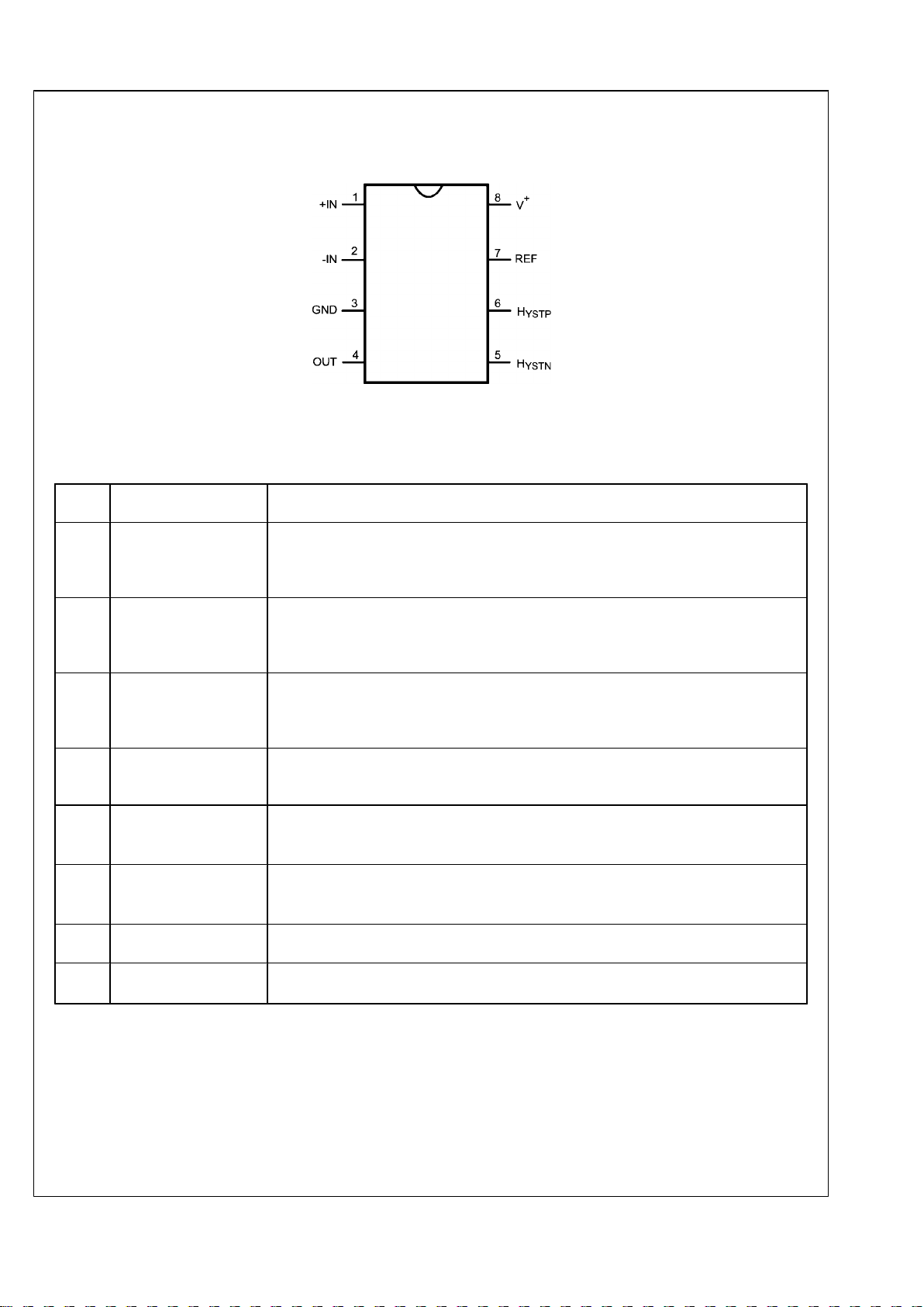
Connection Diagram
8-Pin MSOP/SOIC
20175606
Top View
Pin Descriptions
Pin
Name
Description
+IN Non-Inverting
Comparator Input
The +IN has a common-mode voltage range from 1V above the negative rail to, and including,
the positive rail. Internal ESD diodes, connected from the +IN pin to the rails, protect the input
stage from overvoltage. If the input voltage exceeds the rails, the diodes turn on and clamp
the input to a safe level.
−IN Inverting Comparator
Input
The −IN has a common-mode voltage range from 1V above the negative rail to, and including,
the positive rail. Internal ESD diodes, connected from the −IN pin to the rails, protects the
input stage from overvoltage. If the input voltage exceeds the rails, the diodes turn on and
clamp the input to a safe level.
GND Ground This pin may be connected to a negative DC voltage source for applications requiring a dual
supply. If connected to a negative supply, decouple this pin with 0.1 µF ceramic capacitor to
ground. The internal reference output voltage is referenced to this pin. GND is the die
substrate connection.
OUT Comparator Output The output is an open-collector. It can drive voltage loads by using a pullup resistor, or it can
drive current loads by sinking a maximum output current. This pin may be taken to a
maximum of +12V with respect to the ground pin, irrespective of supply voltage.
HYSTN Negative Hysteresis Pin This pin sets the lower trip voltage VIL. The common mode range is from 1V above the
negative rail to VCC. The input signal must fall below VIL for the comparator to switch from
high to low state.
HYSTP Positive Hysteresis pin This pin sets the upper trip voltage VIH. The common mode range is from 1V above the
negative rail to VCC. The input signal must rise above VIH for the comparator to switch from
low to high state.
REF Reference Voltage
Output Pin
This is the output pin of a 2.048V band gap precision reference.
V
+
Positive Supply Terminal
The supply voltage range is 2.7V to 12V. Decouple this pin with 0.1 μF ceramic capacitor to
ground.
5 www.national.com
LMP7300
Page 6

Typical Performance Characteristics
Supply Current vs. Supply Voltage
20175639
Output Low Voltage vs. Load Current
20175632
Output Low Voltage vs. Load Current
20175633
Output Low Voltage vs. Load Current
20175634
Reference Voltage vs. Supply Voltage
20175635
Reference Voltage vs. Source Current
20175636
www.national.com 6
LMP7300
Page 7

Reference Voltage vs. Sink Current
20175637
Reference Voltage vs. Source Current
20175638
Propagation Delay vs. Overdrive Voltage
20175640
Propagation Delay vs. Overdrive Voltage
20175641
Propagation Delay vs. Overdrive Voltage
20175642
7 www.national.com
LMP7300
Page 8

Application Information
GENERAL DESCRIPTION
The LMP7300 is a unique combination of micropower and
precision. The open collector comparator has low offset, high
CMRR, high PSRR, programmable hysteresis and microamp
supply current. The precision 2.048V reference provides a
DAC or ADC with an accurate binary divisible voltage. The
comparator and reference combination forms an ideal single
IC solution for low power sensor or portable applications.
VOLTAGE REFERENCE
The reference output voltage is a band gap derived 2.048V
that is trimmed to achieve typically 0.2% accuracy over the
full operating temperature range of −40°C to 125°C. The trim
procedure employs a curvature correction algorithm to compensate for the base emitter thermal nonlinearity inherent in
band gap design topologies. The reference accuracy and the
set resistor tolerance determine the magnitude and precision
of the programmable hysteresis. In situations where reference noise filtering is required a 5 µF capacitor in series with
a 190Ω resistor to ground are recommended.
COMPARATOR
Output Stage
The comparator employs an open collector output stage that
can switch microamp loads for micropower precision threshold detection to applications requiring activating a solenoid, a
lamp, or an LED. The wired-OR type output easily interfaces
to TTL, CMOS, or multiple outputs, as in a window comparator
application, over a range of 0.5V to 12V. The output is capable
of driving greater than 10 mA output current and yet maintaining a saturation voltage below 0.4V over temperature. The
supply current increases linearly when driving heavy loads so
a pullup resistor of 100 kΩ or greater is recommended for micropower applications.
Fault Detection Rate
The user’s choice of a pullup resistor and capacitive load determines the minimum response time and the event detection
rate. By optimizing overdrive, the pullup resistor and capactive load fault update rates of 200 kHz to 250 kHz or
greater can be achieved.
HYSTERESIS
False triggering on noise coupled into the signal path is a
common problem for comparator based threshold detectors.
One of the most effective solutions is to add hysteresis. Hysteresis is a circuit signal path characteristic where an amplitude delay is introduced to the normal input. Positive
hysteresis forces the signal to pass the normal switch point
before the output makes a low to high transition while negative
hysteresis does the opposite. This is a memory effect. The
comparator behaves differently based on which direction the
signal is going.
The LM7300 has been designed with a unique way of introducing hysteresis. The set points are completely independent
of each other, the power supply, and the input or output conditions. The HYSTP pin sets positive hysteresis and the
HYSTN pin sets the negative hysteresis in a simple way using
two resistors. The pins can be tied together for the same hysteresis or tied to separate voltage taps for asymmetric hysteresis, or tied to the reference for no hysteresis. When the
precision reference is used to drive the voltage tap resistor
divider precise, stable threshold levels can be obtained. The
maximum recommended hysteresis is about 130 mV. This
places the HYSTP and HYSTN pin voltages at V
REF
– 130 mV
which is approximately the center of their input common mode
range at 2.7V. For the typical example, a differential input
signal voltage, VIN, is applied between INP and INN, the noninverting and inverting inputs of the comparator. A DC switch
or threshold voltage, VTH, is set on the negative input to keep
the output off when the signal is above and on when it goes
below this level. For a precision threshold tie the INN pin to
V
REF
. With the output, off the circuit is in the minimum power
state. Figure 1 through Figure 5 demonstrate the different
configurations for setting the upper threshold VIH and the lower threshold VIL and their relationship to the input trip point
V
REF
, by the following formulas.
20175607
(a)
20175608
(b)
When VID = 0, INN = INP = V
TH
FIGURE 1. Typical Micropower Application to Set
Asymmetric Positive and
Negative Hysteresis of −10 mV, +3 mV
www.national.com 8
LMP7300
Page 9

Figure 2 shows the configuration with no hysteresis when the
HYSTP and HYSTN pins are connected together to V
REF
.
This configuration is not recommended because it has the
highest level of false triggers due to the system noise.
20175611
(a)
20175609
(b)
FIGURE 2. Typical Configuration for No Hysteresis
Figure 3 shows the configuration with symmetric hysteresis
when the HYSTP and HYSTN pins are connected to the same
voltage that is less than V
REF
. The two trip points set a hys-
teresis band around the input threshold voltage V
REF
, such
that the positive band is equal to the negative band.
This configuration controls the false triggering mentioned in
Figure 2. Symmetric hysteresis values less than 5mV to 10
mV are recommended for precise level detection applications.
20175614
(a)
20175612
(b)
FIGURE 3. Symmetric Hysteresis ±5 mV
9 www.national.com
LMP7300
Page 10

Figure 4 shows the case for negative hysteresis by biasing
only the HYSN pin to a voltage less than V
REF
.
20175618
(a)
20175616
(b)
FIGURE 4. Typical Configuration for Negative Hysteresis
= −10 mV
The case for setting only a positive hysteresis is demonstrated in Figure 5.
20175622
(a)
20175620
(b)
FIGURE 5. Connections for Positive Hysteresis = +10 mV
www.national.com 10
LMP7300
Page 11

In the general case, as demonstrated with both positive and
negative hysteresis bands in Figure 6, noise within these
bands will have no affect on the state of the comparator output. In Example #1 the noise is well behaved and in band. The
output is clean and well behaved. In Example #2, a significant
amount of out of band noise is present but due to hysteresis
no false triggers occur on the rising positive or falling negative
edges. The hysteresis forces the signal level to move higher
or lower before the output is set to the opposite state.
20175628
FIGURE 6. Output Response with Input Noise Less than
Hysteresis Band
How Much Hysteresis Is Correct?
An effective way of determining the minimum hysteresis necessary for clean switching is to decrease the amount of hysteresis until false triggering is observed, and then use a
multiple of say three times that amount of hysteresis in the
final circuit. This is most easily accomplished in the bread-
board phase by making R1 and R2 potentiometers. For applications near or above +100°C a minimum of 5 mV hysteresis
is recommended due to peaking of the LMP7300 noise sensitivity at high temperatures.
LAYOUT RECOMMENDATIONS
A good PCB layout is always important to reduce output to
input coupling. Positive feedback noise reduces performance.
For the LMP7300 output coupling is minimized by the unique
package pinout. The output is kept away from the non-inverting and inverting inputs, the reference and the hysteresis pins.
EVALUATION BOARDS
National Semiconductor provides the following PCB boards
as an aid in evaluating the LMP7300 performance.
Device Package Evaluation Board
Ordering ID
LMP7300MA 8-Pin SOIC LMP7300MA-EVAL
LMP7300MM 8-Pin MSOP LMP7300MM-EVAL
WINDOW COMPARATOR
Figure 8 shows two LMP7300s configured as a micropower
window detector in a temperature level detection application.
The circuit shown monitors the ambient temperature change.
If the temperature rises outside the 15°C to 35°C window, either comparator 1 for high temp, or comparator 2 for low temp,
will set low, indicating a fault condition has occurred. The
open collector outputs are pulled up separately but can be
wire-OR’d for a single fault indication. If the temperature returns inside the window it must overcome the 22 mV asymmetric hysteresis band established on either comparator. For
the high side the temperature must drop below 34°C and for
the low side the temperature must rise above 16°C for the
outputs to reset high and remove the fault indication. The
temperature is sensed by a 30 kΩ @ 25°C Omega Precision
NTC Thermistor #44008 (±0.2% tol).
20175629
FIGURE 7. Temperature Controlled Window Detector to Monitor Ambient Temperature
11 www.national.com
LMP7300
Page 12

PRECISION HIGH TEMPERATURE SWITCH
The LMP7300 brings accuracy and stability to simple sensor
switch applications. Figure 9 shows the LMP7300 setup in a
high temperature switch configuration. The input bridge establishes the trip point at 85°C and the reset temperature at
80°C. The comparator is set up with positive hysteresis of
14.3 mV and no negative hysteresis. When the temperature
is rising it trips at 85°C. The 14.3 mV hysteresis allows the
temperature to drop to 80°C before reset.
The temperature sensor used is an Omega 44008 Precision
NTC Thermistor. The 44008 has an accuracy of ±0.2°C. The
resistance at 85°C is 3270.9Ω and at 80°C is 3840.2Ω. The
trip voltage threshold is established by one half of the bridge,
which is the ratio of R
ADJ
and R
SET
. The input signal bias is
set by the second half, which is the ratio of the thermistor resistance RTH and R
SET
. The resistance values are chosen for
∼50 µA bridge current to minimize the power in the thermistor.
The thermistor specification states it has a 1°C/mW dissipa-
tion error. The reference voltage establishes the supply voltage for the bridge to make the circuit independent of supply
voltage variation. Capacitor C1 establishes a low frequency
pole at F
CORNER
= 1/(2πC1*2(R
SET
//R
ADJ
)). With the resistance values chosen C1 should be selected for Fc < 10 Hz.
This will limit the thermal noise in the bridge.
The accuracy of the circuit can be calculated from the nearest
resistance values chosen. For 1% resistors RADJ is 3.24
kΩ, and R
SET
is 78.7 kΩ. The bridge gain becomes
2.488 mV/C at 85°C. In general, the higher the bridge current
is allowed to be, the higher the bridge gain will be. The actual
trip point found during simulation is 85.3°C and the reset point
is 80.04°C. With the values chosen the worst case trip temperature uncertainty is ±1.451°C and the reset uncertainty is
±1.548°C. Accuracy could be maximized with resistors chosen to 0.1% values, 0.1% tolerance and by using the 0.1%
model of the Omega 44008 thermistor.
20175647
FIGURE 8. Precision High Temperature Switch
MICROPOWER PRECISION BATTERY LOW VOLTAGE
DETECTOR
The ability of the LMP7300 to operate at very low supply voltages, makes it an ideal choice for low battery detection application in portable equipment. The circuit in Figure 9
performs the function of low voltage threshold detection in a
3 cell 0.9V discharge voltage, battery monitor application.
R1 and R2 are chosen to set the inverting input voltage equal
to the non-inverting input voltage when the battery voltage is
equal to the minimum operating voltage of the system. Here,
the very precise reference output voltage is directly connected to the non-inverting input on the comparator and sets an
accurate threshold voltage. The hysteresis is set to 0 mV
negative and 20 mV positive. The output is off for voltages
higher than the minimum V
BATT
, and turns on when the circuit
detects a minimum battery voltage condition.
20175631
FIGURE 9. Battery Voltage Monitor for 3 Cell Discharge Voltage
www.national.com 12
LMP7300
Page 13

Physical Dimensions inches (millimeters) unless otherwise noted
8-Pin SOIC
NS Package Number M08A
8-Pin MSOP
NS Package Number MUA08A
13 www.national.com
LMP7300
Page 14

Notes
LMP7300 Micropower Precision Comparator and Precision Reference with Adjustable
Hysteresis
THE CONTENTS OF THIS DOCUMENT ARE PROVIDED IN CONNECTION WITH NATIONAL SEMICONDUCTOR CORPORATION
(“NATIONAL”) PRODUCTS. NATIONAL MAKES NO REPRESENTATIONS OR WARRANTIES WITH RESPECT TO THE ACCURACY
OR COMPLETENESS OF THE CONTENTS OF THIS PUBLICATION AND RESERVES THE RIGHT TO MAKE CHANGES TO
SPECIFICATIONS AND PRODUCT DESCRIPTIONS AT ANY TIME WITHOUT NOTICE. NO LICENSE, WHETHER EXPRESS,
IMPLIED, ARISING BY ESTOPPEL OR OTHERWISE, TO ANY INTELLECTUAL PROPERTY RIGHTS IS GRANTED BY THIS
DOCUMENT.
TESTING AND OTHER QUALITY CONTROLS ARE USED TO THE EXTENT NATIONAL DEEMS NECESSARY TO SUPPORT
NATIONAL’S PRODUCT WARRANTY. EXCEPT WHERE MANDATED BY GOVERNMENT REQUIREMENTS, TESTING OF ALL
PARAMETERS OF EACH PRODUCT IS NOT NECESSARILY PERFORMED. NATIONAL ASSUMES NO LIABILITY FOR
APPLICATIONS ASSISTANCE OR BUYER PRODUCT DESIGN. BUYERS ARE RESPONSIBLE FOR THEIR PRODUCTS AND
APPLICATIONS USING NATIONAL COMPONENTS. PRIOR TO USING OR DISTRIBUTING ANY PRODUCTS THAT INCLUDE
NATIONAL COMPONENTS, BUYERS SHOULD PROVIDE ADEQUATE DESIGN, TESTING AND OPERATING SAFEGUARDS.
EXCEPT AS PROVIDED IN NATIONAL’S TERMS AND CONDITIONS OF SALE FOR SUCH PRODUCTS, NATIONAL ASSUMES NO
LIABILITY WHATSOEVER, AND NATIONAL DISCLAIMS ANY EXPRESS OR IMPLIED WARRANTY RELATING TO THE SALE
AND/OR USE OF NATIONAL PRODUCTS INCLUDING LIABILITY OR WARRANTIES RELATING TO FITNESS FOR A PARTICULAR
PURPOSE, MERCHANTABILITY, OR INFRINGEMENT OF ANY PATENT, COPYRIGHT OR OTHER INTELLECTUAL PROPERTY
RIGHT.
LIFE SUPPORT POLICY
NATIONAL’S PRODUCTS ARE NOT AUTHORIZED FOR USE AS CRITICAL COMPONENTS IN LIFE SUPPORT DEVICES OR
SYSTEMS WITHOUT THE EXPRESS PRIOR WRITTEN APPROVAL OF THE CHIEF EXECUTIVE OFFICER AND GENERAL
COUNSEL OF NATIONAL SEMICONDUCTOR CORPORATION. As used herein:
Life support devices or systems are devices which (a) are intended for surgical implant into the body, or (b) support or sustain life and
whose failure to perform when properly used in accordance with instructions for use provided in the labeling can be reasonably expected
to result in a significant injury to the user. A critical component is any component in a life support device or system whose failure to perform
can be reasonably expected to cause the failure of the life support device or system or to affect its safety or effectiveness.
National Semiconductor and the National Semiconductor logo are registered trademarks of National Semiconductor Corporation. All other
brand or product names may be trademarks or registered trademarks of their respective holders.
Copyright© 2007 National Semiconductor Corporation
For the most current product information visit us at www.national.com
National Semiconductor
Americas Customer
Support Center
Email:
new.feedback@nsc.com
Tel: 1-800-272-9959
National Semiconductor Europe
Customer Support Center
Fax: +49 (0) 180-530-85-86
Email: europe.support@nsc.com
Deutsch Tel: +49 (0) 69 9508 6208
English Tel: +49 (0) 870 24 0 2171
Français Tel: +33 (0) 1 41 91 8790
National Semiconductor Asia
Pacific Customer Support Center
Email: ap.support@nsc.com
National Semiconductor Japan
Customer Support Center
Fax: 81-3-5639-7507
Email: jpn.feedback@nsc.com
Tel: 81-3-5639-7560
www.national.com
 Loading...