

Page 1
February 7, 2008
LMP2231 Single
Micropower, 1.8V, Precision Operational Amplifier with
CMOS Inputs
General Description
The LMP2231 is a single micropower precision amplifier designed for battery powered applications. The 1.8V to 5.0V
guaranteed supply voltage range and quiescent power consumption of only 18 μW extend the battery life in portable
battery operated systems. The LMP2231 is part of the
LMP® precision amplifier family. The high impedance CMOS
input makes it ideal for instrumentation and other sensor interface applications.
The LMP2231 has a maximum offset of 150 µV and maximum
offset voltage drift of only 0.4 µV/°C along with low bias current of only ±20 fA. These precise specifications make the
LMP2231 a great choice for maintaining system accuracy and
long term stability.
The LMP2231 has a rail-to-rail output that swings 15 mV from
the supply voltage, which increases system dynamic range.
The common mode input voltage range extends 200 mV below the negative supply, thus the LMP2231 is ideal for use in
single supply applications with ground sensing.
The LMP2231 is offered in 5-Pin SOT23 and 8-pin SOIC
packages.
The dual and quad versions of this product are also available.
The dual, LMP2232 is offered in 8-pin SOIC and MSOP. The
quad, LMP2234 is offered in 14-pin SOIC and TSSOP.
Features
(For VS = 5V, Typical unless otherwise noted)
■
Supply current 10 µA
■
Operating voltage range 1.6V to 5.5V
■
Low TCV
OS
±0.4 µV/°C (max)
■
V
OS
±150 µV (max)
■
Input bias current 20 fA
■
PSRR 120 dB
■
CMRR 97 dB
■
Open loop gain 120 dB
■
Gain bandwidth product 130 kHz
■
Slew rate 58 V/ms
■
Input voltage noise, f = 1 kHz 60 nV/√Hz
■
Temperature range –40°C to 125°C
Applications
■
Precision instrumentation amplifiers
■
Battery powered medical instrumentation
■
High Impedance Sensors
■
Strain gauge bridge amplifier
■
Thermocouple amplifiers
Typical Application
30033874
Strain Gauge Bridge Amplifier
LMP® is a registered trademark of National Semiconductor Corporation.
© 2008 National Semiconductor Corporation 300338 www.national.com
LMP2231 Single Micropower, 1.8V, Precision, Operational Amplifier with CMOS Inputs
Page 2

Absolute Maximum Ratings (Note 1)
If Military/Aerospace specified devices are required,
please contact the National Semiconductor Sales Office/
Distributors for availability and specifications.
ESD Tolerance (Note 2)
Human Body Model 2000V
Machine Model 100V
Differential Input Voltage ±300 mV
Supply Voltage (VS = V+ - V–)
6V
Voltage on Input/Output Pins V+ + 0.3V, V– – 0.3V
Storage Temperature Range −65°C to 150°C
Junction Temperature (Note 3) 150°C
Mounting Temperature
Infrared or Convection (20 sec.) +235°C
Operating Ratings (Note 1)
Operating Temperature Range (Note 3) −40°C to 125°C
Supply Voltage (VS = V+ - V−)
1.6V to 5.5V
Package Thermal Resistance (θJA) (Note 3)
5-Pin SOT23 160.6 °C/W
8-Pin SOIC 116.2 °C/W
5V DC Electrical Characteristics (Note 4) Unless otherwise specified, all limits guaranteed for T
A
= 25°C,
V+ = 5V, V− = 0V, V
CM
= VO = V+/2, and RL > 1 MΩ. Boldface limits apply at the temperature extremes.
Symbol Parameter Conditions Min
(Note 6)
Typ
(Note 5)
Max
(Note 6)
Units
V
OS
Input Offset Voltage ±10 ±150
±230
μV
TCV
OS
Input Offset Voltage Drift LMP2231A ±0.3 ±0.4
μV/°C
LMP2231B ±0.3 ±2.5
I
BIAS
Input Bias Current 0.02 ±1
±50
pA
I
OS
Input Offset Current 5 fA
CMRR Common Mode Rejection Ratio
0V ≤ VCM ≤ 4V
81
80
97
dB
PSRR Power Supply Rejection Ratio
1.6V ≤ V+ ≤ 5.5V
V− = 0V, VCM = 0V
83
83
120
dB
CMVR Common Mode Voltage Range
CMRR ≥ 80 dB
CMRR ≥ 79 dB
−0.2
−0.2
4.2
4.2
V
A
VOL
Large Signal Voltage Gain VO = 0.3V to 4.7V
RL = 10 kΩ to V+/2
110
108
120
dB
V
O
Output Swing High
RL = 10 kΩ to V+/2
VIN(diff) = 100 mV
17 50
50
mV
from either
rail
Output Swing Low
RL = 10 kΩ to V+/2
VIN(diff) = −100 mV
17 50
50
I
O
Output Current (Note 7) Sourcing, VO to V
–
VIN(diff) = 100 mV
27
19
30
mA
Sinking, VO to V
+
VIN(diff) = −100 mV
17
12
22
I
S
Supply Current 10 16
18
µA
5V AC Electrical Characteristics (Note 4) Unless otherwise specified, all limits guaranteed for T
A
= 25°C,
V+ = 5V, V− = 0V, VCM = VO = V+/2, and RL > 1 MΩ. Boldface limits apply at the temperature extremes.
Symbol Parameter Conditions Min
(Note 6)
Typ
(Note 5)
Max
(Note 6)
Units
GBW Gain-Bandwidth Product
CL = 20 pF, RL = 10 kΩ
130 kHz
SR Slew Rate AV = +1 Falling Edge 33
32
58
V/ms
Rising Edge 33
32
48
θ
m
Phase Margin
CL = 20 pF, RL = 10 kΩ
78 deg
G
m
Gain Margin
CL = 20 pF, RL = 10 kΩ
27
dB
www.national.com 2
LMP2231 Single
Page 3

Symbol Parameter Conditions Min
(Note 6)
Typ
(Note 5)
Max
(Note 6)
Units
e
n
Input-Referred Voltage Noise Density f = 1 kHz 60
nV/
Input-Referred Voltage Noise 0.1 Hz to 10 Hz 2.3
μV
PP
i
n
Input-Referred Current Noise f = 1 kHz 10
fA/
THD+N Total Harmonic Distortion + Noise
f = 100 Hz, RL = 10 kΩ
0.002
%
3.3V DC Electrical Characteristics (Note 4) Unless otherwise specified, all limits guaranteed for
TA = 25°C, V+ = 3.3V, V− = 0V, V
CM
= VO = V+/2, and RL > 1 MΩ. Boldface limits apply at the temperature extremes.
Symbol Parameter Conditions Min
(Note 6)
Typ
(Note 5)
Max
(Note 6)
Units
V
OS
Input Offset Voltage ±10 ±160
±250
μV
TCV
OS
Input Offset Voltage Drift LMP2231A ±0.3 ±0.4
μV/°C
LMP2231B ±0.3 ±2.5
I
BIAS
Input Bias Current 0.02 ±1
±50
pA
I
OS
Input Offset Current 5 fA
CMRR Common Mode Rejection Ratio
0V ≤ VCM ≤ 2.3V
79
77
92
dB
PSRR Power Supply Rejection Ratio
1.6V ≤ V+ ≤ 5.5V
V− = 0V, VCM = 0V
83
83
120
dB
CMVR Common Mode Voltage Range
CMRR ≥ 78 dB
CMRR ≥ 77 dB
−0.2
−0.2
2.5
2.5
V
A
VOL
Large Signal Voltage Gain VO = 0.3V to 3V
RL = 10 kΩ to V+/2
108
107
120
dB
V
O
Output Swing High
RL = 10 kΩ to V+/2
VIN(diff) = 100 mV
14 50
50
mV
from either
rail
Output Swing Low
RL = 10 kΩ to V+/2
VIN(diff) = −100 mV
14 50
50
I
O
Output Current (Note 7) Sourcing, VO to V
–
VIN(diff) = 100 mV
11
8
14
mA
Sinking, VO to V
+
VIN(diff) = −100 mV
8
5
11
I
S
Supply Current 10 15
16
µA
3.3V AC Electrical Characteristics (Note 4) Unless otherwise is specified, all limits guaranteed for
TA = 25°C, V+ = 3.3V, V− = 0V, VCM = VO = V+/2, and RL > 1 MΩ. Boldface limits apply at the temperature extremes.
Symbol Parameter Conditions Min
(Note 6)
Typ
(Note 5)
Max
(Note 6)
Units
GBW Gain-Bandwidth Product
CL = 20 pF, RL = 10 kΩ
128 kHz
SR Slew Rate AV = +1, CL = 20 pF
RL = 10 kΩ
Falling Edge 58
V/ms
Rising Edge 48
θ
m
Phase Margin
CL = 20 pF, RL = 10 kΩ
76 deg
G
m
Gain Margin
CL = 20 pF, RL = 10 kΩ
26 dB
e
n
Input-Referred Voltage Noise Density f = 1 kHz 60
nV/
Input-Referred Voltage Noise 0.1 Hz to 10 Hz 2.4
μV
PP
i
n
Input-Referred Current Noise f = 1 kHz 10
fA/
THD+N Total Harmonic Distortion + Noise
f = 100 Hz, RL = 10 kΩ
0.003
%
3 www.national.com
LMP2231 Single
Page 4
2.5V DC Electrical Characteristics (Note 4) Unless otherwise specified, all limits guaranteed for
TA = 25°C, V+ = 2.5V, V− = 0V, VCM = VO = V+/2, and RL > 1MΩ. Boldface limits apply at the temperature extremes.
Symbol Parameter Conditions Min
(Note 6)
Typ
(Note 5)
Max
(Note 6)
Units
V
OS
Input Offset Voltage ±10 ±190
±275
μV
TCV
OS
Input Offset Voltage Drift LMP2231A ±0.3 ±0.4
μV/°C
LMP2231B ±0.3 ±2.5
I
BIAS
Input Bias Current 0.02 ±1.0
±50
pA
I
OS
Input Offset Current 5 fA
CMRR Common Mode Rejection Ratio
0V ≤ VCM ≤ 1.5V
77
76
91
dB
PSRR Power Supply Rejection Ratio
1.6V ≤ V+ ≤ 5.5V
V− = 0V, VCM = 0V
83
83
120
dB
CMVR Common Mode Voltage Range
CMRR ≥ 77 dB
CMRR ≥ 76 dB
−0.2
−0.2
1.7
1.7
V
A
VOL
Large Signal Voltage Gain VO = 0.3V to 2.2V
RL = 10 kΩ to V+/2
104
104
120
dB
V
O
Output Swing High
RL = 10 kΩ to V+/2
VIN(diff) = 100 mV
12 50
50
mV
from either
rail
Output Swing Low
RL = 10 kΩ to V+/2
VIN (diff) = −100 mV
13 50
50
I
O
Output Current (Note 7) Sourcing, VO to V
−
VIN(diff) = 100 mV
5
4
8
mA
Sinking, VO to V
+
VIN(diff) = −100 mV
3.5
2.5
7
I
S
Supply Current 10 14
15
µA
2.5V AC Electrical Characteristics (Note 4) Unless otherwise specified, all limits guaranteed for
TA = 25°C, V+ = 2.5V, V− = 0V, VCM = VO = V+/2, and RL > 1MΩ. Boldface limits apply at the temperature extremes.
Symbol Parameter Conditions Min
(Note 6)
Typ
(Note 5)
Max
(Note 6)
Units
GBW Gain-Bandwidth Product
CL = 20 pF, RL = 10 kΩ
128 kHz
SR Slew Rate AV = +1, CL = 20 pF
RL = 10 kΩ
Falling Edge 58
V/ms
Rising Edge 48
θ
m
Phase Margin
CL = 20 pF, RL = 10 kΩ
74 deg
G
m
Gain Margin
CL = 20 pF, RL = 10 kΩ
26
dB
e
n
Input-Referred Voltage Noise Density f = 1 kHz 60
nV/
Input-Referred Voltage Noise 0.1 Hz to 10 Hz 2.5
μV
PP
i
n
Input-Referred Current Noise f = 1 kHz 10
fA/
THD+N Total Harmonic Distortion + Noise
f = 100 Hz, RL = 10 kΩ
0.005
%
www.national.com 4
LMP2231 Single
Page 5
1.8V DC Electrical Characteristics (Note 4) Unless otherwise specified, all limits guaranteed for
TA = 25°C, V+ = 1.8V, V− = 0V, VCM = VO = V+/2, and RL > 1 MΩ. Boldface limits apply at the temperature extremes.
Symbol Parameter Conditions Min
(Note 6)
Typ
(Note 5)
Max
(Note 6)
Units
V
OS
Input Offset Voltage ±10 ±230
±325
μV
TCV
OS
Input Offset Voltage Drift LMP2231A ±0.3 ±0.4
μV/°C
LMP2231B ±0.3 ±2.5
I
BIAS
Input Bias Current 0.02 ±1.0
±50
pA
I
OS
Input Offset Current 5
fA
CMRR Common Mode Rejection Ratio
0V ≤ VCM ≤ 0.8V
76
75
92
dB
PSRR Power Supply Rejection Ratio
1.6V ≤ V+ ≤ 5.5V
V− = 0V, VCM = 0V
83
83
120
dB
CMVR Common Mode Voltage Rang
CMRR ≥ 76 dB
CMRR ≥ 75 dB
−0.2
0
1.0
1.0
V
A
VOL
Large Signal Voltage Gain VO = 0.3V to 1.5V
RL = 10 kΩ to V+/2
103
103
120
dB
V
O
Output Swing High
RL = 10 kΩ to V+/2
VIN(diff) = 100 mV
12 50
50
mV
from either
rail
Output Swing Low
RL = 10 kΩ to V+/2
VIN(diff) = −100 mV
13 50
50
I
O
Output Current (Note 7) Sourcing, VO to V
−
VIN(diff) = 100 mV
2.5
2
5
mA
Sinking, VO to V
+
VIN(diff) = −100 mV
2
1.5
5
I
S
Supply Current 10 14
15
µA
1.8V AC Electrical Characteristics (Note 4) Unless otherwise is specified, all limits guaranteed for
TA = 25°C, V+ = 1.8V, V− = 0V, VCM = VO = V+/2, and RL > 1 MΩ. Boldface limits apply at the temperature extremes.
Symbol Parameter Conditions Min
(Note 6)
Typ
(Note 5)
Max
(Note 6)
Units
GBW Gain-Bandwidth Product
CL = 20 pF, RL = 10 kΩ
127 kHz
SR Slew Rate AV = +1, CL = 20 pF
RL = 10 kΩ
Falling Edge 58
V/ms
Rising Edge 48
θ
m
Phase Margin
CL = 20 pF, RL = 10 kΩ
70 deg
G
m
Gain Margin
CL = 20 pF, RL = 10 kΩ
25
dB
e
n
Input-Referred Voltage Noise Density f = 1 kHz 60
nV/
Input-Referred Voltage Noise 0.1 Hz to 10 Hz 2.4
μV
PP
i
n
Input-Referred Current Noise f = 1 kHz 10
fA/
THD+N Total Harmonic Distortion + Noise
f = 100 Hz, RL = 10 kΩ
0.005 %
5 www.national.com
LMP2231 Single
Page 6
Note 1: Absolute Maximum Ratings indicate limits beyond which damage may occur. Operating Ratings indicate conditions for which the device is intended to
be functional, but specific performance is not guaranteed. For guaranteed specifications and test conditions, see the Electrical Characteristics.
Note 2: Human Body Model, applicable std. MIL-STD-883, Method 3015.7. Machine Model, applicable std. JESD22-A115-A (ESD MM std. of JEDEC)
Field-Induced Charge-Device Model, applicable std. JESD22-C101-C (ESD FICDM std. of JEDEC).
Note 3: The maximum power dissipation is a function of T
J(MAX)
, θJA. The maximum allowable power dissipation at any ambient temperature is
PD = (T
J(MAX)
– TA)/ θJA. All numbers apply for packages soldered directly onto a PC Board.
Note 4: Electrical Table values apply only for factory testing conditions at the temperature indicated. Factory testing conditions result in very limited self-heating
of the device such that TJ = TA. No guarantee of parametric performance is indicated in the electrical tables under conditions of internal self-heating where TJ >
TA. Absolute Maximum Ratings indicate junction temperature limits beyond which the device may be permanently degraded, either mechanically or electrically.
Note 5: Typical values represent the most likely parametric norm at the time of characterization. Actual typical values may vary over time and will also depend
on the application and configuration. The typical values are not tested and are not guaranteed on shipped production material.
Note 6: All limits are guaranteed by testing, statistical analysis or design.
Note 7: The short circuit test is a momentary open loop test.
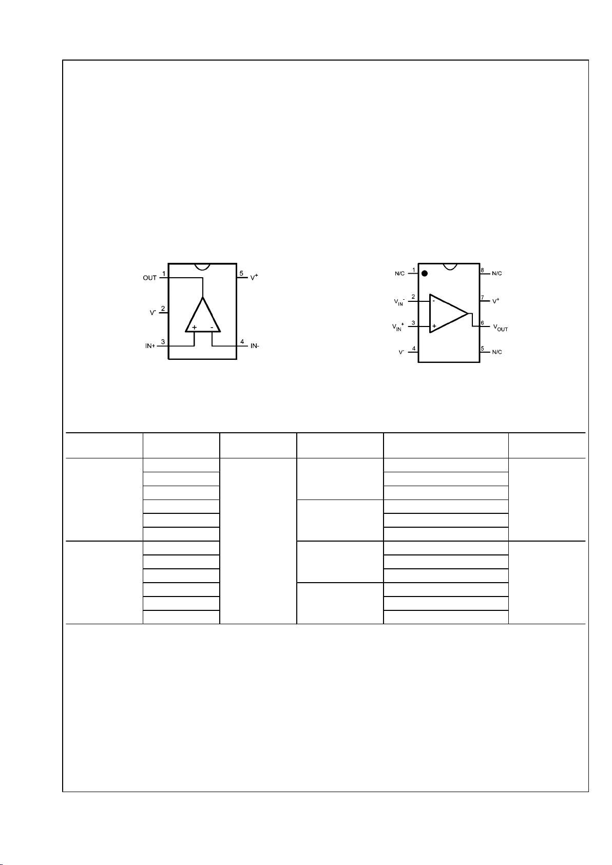
Connection Diagrams
5-Pin SOT23
30033802
Top View
8-Pin SOIC
30033842
Top View
Ordering Information
Package Part Number Temperature
Range
Package Marking Transport Media NSC Drawing
5-Pin SOT23
LMP2231AMF
−40°C to 125°C
AL5A
1k Units Tape and Reel
MF05A
LMP2231AMFE 250 Units Tape and Reel
LMP2231AMFX 3k Units Tape and Reel
LMP2231BMF
AL5B
1k Units Tape and Reel
LMP2231BMFE 250 Units Tape and Reel
LMP2231BMFX 3k Units Tape and Reel
8-Pin SOIC
LMP2231AMA
LMP2231AMA
95 Units/Rail
M08A
LMP2231AMAE 250 Units Tape and Reel
LMP2231AMAX 2.5k Units Tape and Reel
LMP2231BMA
LMP2231BMA
95 Units/Rail
LMP2231BMAE 250 Units Tape and Reel
LMP2231BMAX 2.5k Units Tape and Reel
www.national.com 6
LMP2231 Single
Page 7

Typical Performance Characteristics Unless otherwise Specified: T
A
= 25°C, VS = 5V, VCM = VS/2, where
VS = V+ - V
−
Offset Voltage Distribution
30033807
TCVOS Distribution
30033811
Offset Voltage Distribution
30033806
TCVOS Distribution
30033810
Offset Voltage Distribution
30033805
TCVOS Distribution
30033809
7 www.national.com
LMP2231 Single
Page 8

Offset Voltage Distribution
30033873
TCVOS Distribution
30033869
Offset Voltage vs. V
CM
30033818
Offset Voltage vs. V
CM
30033865
Offset Voltage vs. V
CM
30033864
Offset Voltage vs. V
CM
30033872
www.national.com 8
LMP2231 Single
Page 9

Offset Voltage vs. Temperature
30033871
Offset Voltage vs. Supply Voltage
30033870
Time Domain Voltage Noise
30033833
Time Domain Voltage Noise
30033834
Time Domain Voltage Noise
30033832
Time Domain Voltage Noise
30033831
9 www.national.com
LMP2231 Single
Page 10

Input Bias Current vs. V
CM
30033855
Input Bias Current vs. V
CM
30033856
Input Bias Current vs. V
CM
30033857
Input Bias Current vs. V
CM
30033858
Input Bias Current vs. V
CM
30033859
Input Bias Current vs. V
CM
30033860
www.national.com 10
LMP2231 Single
Page 11

Input Bias Current vs. V
CM
30033861
Input Bias Current vs. V
CM
30033862
PSRR vs. Frequency
30033866
Supply Current vs. Supply Voltage
30033812
Sinking Current vs. Supply Voltage
30033813
Sourcing Current vs. Supply Voltage
30033814
11 www.national.com
LMP2231 Single
Page 12

Output Swing High vs. Supply Voltage
30033815
Output Swing Low vs. Supply Voltage
30033816
Open Loop Frequency Response
30033821
Open Loop Frequency Response
30033822
Phase Margin vs. Capacitive Load
30033863
Slew Rate vs. Supply Voltage
30033830
www.national.com 12
LMP2231 Single
Page 13

THD+N vs. Amplitude
30033828
THD+N vs. Frequency
30033829
Large Signal Step Response
30033824
Small Signal Step Response
30033823
Large Signal Step Response
30033826
Small Signal Step Response
30033825
13 www.national.com
LMP2231 Single
Page 14

CMRR vs. Frequency
30033867
Input Voltage Noise vs. Frequency
30033819
www.national.com 14
LMP2231 Single
Page 15

Application Information
LMP2231
The LMP2231 is a single CMOS precision amplifier that offer
low offset voltage and low offset voltage drift, and high gain
while only consuming 10 μA of current per channel.
The LMP2231 is a micropower op amp, consuming only
10 μA of current. Micropower op amps extend the run time of
battery powered systems and reduce energy consumption in
energy limited systems. The guaranteed supply voltage range
of 1.8V to 5.0V along with the ultra-low supply current extend
the battery run time in two ways. The extended guaranteed
power supply voltage range of 1.8V to 5.0V enables the op
amp to function when the battery voltage has depleted from
its nominal value down to 1.8V. In addition, the lower power
consumption increases the life of the battery.
The LMP2231 has an input referred offset voltage of only
±150 μV maximum at room temperature. This offset is guaranteed to be less than ±230 μV over temperature. This minimal offset voltage along with very low TCVOS of only
0.3 µV/°C typical allows more accurate signal detection and
amplification in precision applications.
The low input bias current of only ±20 fA gives the LMP2231
superiority for use in high impedance sensor applications.
Bias Current of an amplifier flows through source resistance
of the sensor and the voltage resulting from this current flow
appears as a noise voltage on the input of the amplifier. The
low input bias current enables the LMP2231 to interface with
high impedance sensors while generating negligible voltage
noise. Thus the LMP2231 provides better signal fidelity and
a higher signal-to-noise ration when interfacing with high
impedance sensors.
National Semiconductor is heavily committed to precision
amplifiers and the market segment they serve. Technical support and extensive characterization data is available for sensitive applications or applications with a constrained error
budget.
The operating supply voltage range of 1.8V to 5.5V over the
extensive temperature range of −40°C to 125°C makes the
LMP2231 an excellent choice for low voltage precision applications with extensive temperature requirements.
The LMP2231 is offered in the space saving 5-Pin SOT23 and
8-pin SOIC package. These small packages are ideal solutions for area constrained PC boards and portable electronics.
TOTAL NOISE CONTRIBUTION
The LMP2231 has a very low input bias current, very low input
current noise, and low input voltage noise for micropower
amplifier. As a result, this amplifier makes a great choice for
circuits with high impedance sensor applications.
Figure 1 shows the typical input noise of the LMP2231 as a
function of source resistance where:
en denotes the input referred voltage noise
ei is the voltage drop across source resistance due to input
referred current noise or ei = RS * i
n
et shows the thermal noise of the source resistance
eni shows the total noise on the input.
Where:
The input current noise of the LMP2231 is so low that it will
not become the dominant factor in the total noise unless
source resistance exceeds 300 MΩ, which is an unrealistically high value. As is evident in Figure 1, at lower RS values,
total noise is dominated by the amplifier’s input voltage noise.
Once RS is larger than a 100 kΩ, then the dominant noise
factor becomes the thermal noise of RS. As mentioned before,
the current noise will not be the dominant noise factor for any
practical application.
30033848
FIGURE 1. Total Input Noise
VOLTAGE NOISE REDUCTION
The LMP2231 has an input voltage noise of 60 nV/
. While
this value is very low for micropower amplifiers, this input
voltage noise can be further reduced by placing N amplifiers
in parallel as shown in Figure 2. The total voltage noise on the
output of this circuit is divided by the square root of the number of amplifiers used in this parallel combination. This is
because each individual amplifier acts as an independent
noise source, and the average noise of independent sources
is the quadrature sum of the independent sources divided by
the number of sources. For N identical amplifiers, this means:
15 www.national.com
LMP2231 Single
Page 16

Figure 2 shows a schematic of this input voltage noise reduction circuit. Typical resistor values are: RG = 10Ω, RF = 1 kΩ,
and RO = 1 kΩ.
30033846
FIGURE 2. Noise Reduction Circuit
PRECISION INSTRUMENTATION AMPLIFIER
Measurement of very small signals with an amplifier requires
close attention to the input impedance of the amplifier, gain
of the overall signal on the inputs, and the gain on each input
of the amplifier. This is because the difference of the input
signal on the two inputs is of the interest and the common
signal is considered noise. A classic circuit implementation is
an instrumentation amplifier. Instrumentation amplifiers have
a finite, accurate, and stable gain. They also have extremely
high input impedances and very low output impedances. Finally they have an extremely high CMRR so that the amplifier
can only respond to the differential signal. A typical instrumentation amplifier is shown in Figure 3.
30033836
FIGURE 3. Instrumentation Amplifier
There are two stages in this amplifier. The last stage, output
stage, is a differential amplifier. In an ideal case the two amplifiers of the first stage, input stage, would be set up as
buffers to isolate the inputs. However they cannot be connected as followers because of mismatch of amplifiers. That
is why there is a balancing resistor between the two. The
product of the two stages of gain will give the gain of the instrumentation amplifier. Ideally, the CMRR should be infinite.
However the output stage has a small non-zero common
mode gain which results from resistor mismatch.
In the input stage of the circuit, current is the same across all
resistors. This is due to the high input impedance and low
input bias current of the LMP2231.
(1)
By Ohm’s Law:
(2)
However:
(3)
So we have:
VO1–VO2 = (2a+1)(V1–V2) (4)
Now looking at the output of the instrumentation amplifier:
(5)
Substituting from Equation 4:
(6)
This shows the gain of the instrumentation amplifier to be:
−K(2a+1)
Typical values for this circuit can be obtained by setting:
a = 12 and K= 4. This results in an overall gain of −100.
www.national.com 16
LMP2231 Single
Page 17

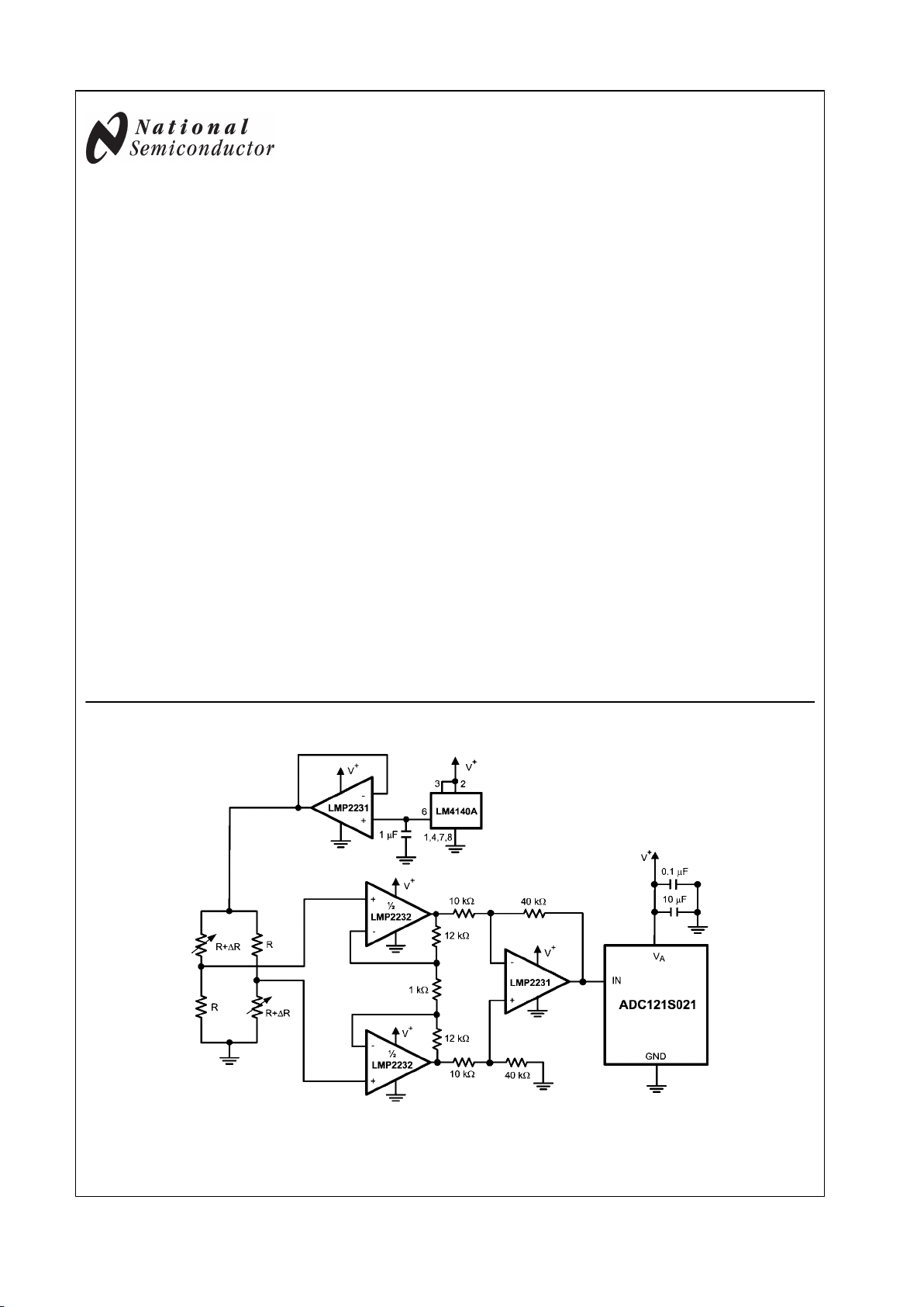
SINGLE SUPPLY STRAIN GAGE BRIDGE AMPLIFIER
Strain gauges are popular electrical elements used to measure force or pressure. Strain gauges are subjected to an
unknown force which is measured as a the deflection on a
previously calibrated scale. Pressure is often measured using
the same technique; however this pressure needs to be converted into force using an appropriate transducer. Strain
gauges are often resistors which are sensitive to pressure or
to flexing. Sense resistor values range from tens of ohms to
several hundred kilo ohms. The resistance change which is a
result of applied force across the strain gauge might be 1% of
its total value. An accurate and reliable system is needed to
measure this small resistance change. Bridge configurations
offer a reliable method for this measurement.
Bridge sensors are formed of four resistors, connected as a
quadrilateral. A voltage source or a current source is used
across one of the diagonals to excite the bridge while a voltage detector across the other diagonal measures the output
voltage.
Bridges are mainly used as null circuits or to measure a differential voltages. Bridges will have no output voltage if the
ratios of two adjacent resistor values are equal. This fact is
used in null circuit measurements. These are particularly
used in feedback systems which involve electrochemical elements or human interfaces. Null systems force an active
resistor, such as a strain gauge, to balance the bridge by influencing the measured parameter.
Often in sensor applications at lease one of the resistors is a
variable resistor, or a sensor. The deviation of this active element from its initial value is measured as an indication of
change in the measured quantity. A change in output voltage
represents the sensor value change. Since the sensor value
change is often very small, the resulting output voltage is very
small in magnitude as well. This requires an extensive and
very precise amplification circuitry so that signal fidelity does
not change after amplification.
Sensitivity of a bridge is the ratio of its maximum expected
output change to the excitation voltage change.
Figure 4 (a) shows a typical bridge sensor and Figure 4(b)
shows the bridge with four sensors. R in Figure 4(b) is the
nominal value of the sense resistor and the deviations from R
are proportional to the quantity being measured.
30033850
30033851
FIGURE 4. Bridge Sensor
Instrumentation amplifiers are great for interfacing with bridge
sensors. Bridge sensors often sense a very small differential
signal in the presence of a larger common mode voltage. Instrumentation amplifiers reject this common mode signal.
Figure 5 shows a strain gauge bridge amplifier. In this application the LMP2231 is used to buffer the LM4140's precision
output voltage. The LM4140A is a precision voltage refer-
ence. The other three LMP2231s are used to form an instrumentation amplifier. This instrumentation amplifier uses the
LMP2231's high CMRR and low VOS and TCVOS to accurately
amplify the small differential signal generated by the output of
the bridge sensor. This amplified signal is then fed into the
ADC121S021 which is a 12-bit analog to digital converter.
This circuit works on a single supply voltage of 5V.
17 www.national.com
LMP2231 Single
Page 18

30033874
FIGURE 5. Strain Gauge Bridge Amplifier
PORTABLE GAS DETECTION SENSOR
Gas sensors are used in many different industrial and medical
applications. They generate a current which is proportional to
the percentage of a particular gas sensed in an air sample.
This current goes through a load resistor and the resulting
voltage drop is measured. Depending on the sensed gas and
sensitivity of the sensor, the output current can be in the order
of tens of microamperes to a few milliamperes. Gas sensor
datasheets often specify a recommended load resistor value
or they suggest a range of load resistors to choose from.
Oxygen sensors are used when air quality or oxygen delivered to a patient needs to be monitored. Fresh air contains
20.9% oxygen. Air samples containing less than 18% oxygen
are considered dangerous. Oxygen sensors are also used in
industrial applications where the environment must lack oxygen. An example is when food is vacuum packed. There are
two main categories of oxygen sensors, those which sense
oxygen when it is abundantly present (i.e. in air or near an
oxygen tank) and those which detect traces of oxygen in ppm.
Figure 6 shows a typical circuit used to amplify the output of
an oxygen detector. The LMP2231 makes an excellent choice
for this application as it only draws 10 µA of current and operates on supply voltages down to 1.8V. This application
detects oxygen in air. The oxygen sensor outputs a known
current through the load resistor. This value changes with the
amount of oxygen present in the air sample. Oxygen sensors
usually recommend a particular load resistor value or specify
a range of acceptable values for the load resistor. Oxygen
sensors typically have a life of one to two years. The use of
the micropower LMP2231 means minimal power usage by the
op amp and it enhances the battery life. Depending on other
components present in the circuit design, the battery could
last for the entire life of the oxygen sensor. The precision
specifications of the LMP2231, such as its very low offset
voltage, low TCVOS , low input bias current, low CMRR, and
low PSRR are other factors which make the LMP2231 a great
choice for this application.
30033849
FIGURE 6. Precision Oxygen Sensor
www.national.com 18
LMP2231 Single
Page 19

Physical Dimensions inches (millimeters) unless otherwise noted
5-Pin SOT23
NS Package Number MF0A5
8-Pin SOIC
NS Package Number M08A
19 www.national.com
LMP2231 Single
Page 20

Notes
LMP2231 Single Micropower, 1.8V, Precision, Operational Amplifier with CMOS Inputs
For more National Semiconductor product information and proven design tools, visit the following Web sites at:
Products Design Support
Amplifiers www.national.com/amplifiers WEBENCH www.national.com/webench
Audio www.national.com/audio Analog University www.national.com/AU
Clock Conditioners www.national.com/timing App Notes www.national.com/appnotes
Data Converters www.national.com/adc Distributors www.national.com/contacts
Displays www.national.com/displays Green Compliance www.national.com/quality/green
Ethernet www.national.com/ethernet Packaging www.national.com/packaging
Interface www.national.com/interface Quality and Reliability www.national.com/quality
LVDS www.national.com/lvds Reference Designs www.national.com/refdesigns
Power Management www.national.com/power Feedback www.national.com/feedback
Switching Regulators www.national.com/switchers
LDOs www.national.com/ldo
LED Lighting www.national.com/led
PowerWise www.national.com/powerwise
Serial Digital Interface (SDI) www.national.com/sdi
Temperature Sensors www.national.com/tempsensors
Wireless (PLL/VCO) www.national.com/wireless
THE CONTENTS OF THIS DOCUMENT ARE PROVIDED IN CONNECTION WITH NATIONAL SEMICONDUCTOR CORPORATION
(“NATIONAL”) PRODUCTS. NATIONAL MAKES NO REPRESENTATIONS OR WARRANTIES WITH RESPECT TO THE ACCURACY
OR COMPLETENESS OF THE CONTENTS OF THIS PUBLICATION AND RESERVES THE RIGHT TO MAKE CHANGES TO
SPECIFICATIONS AND PRODUCT DESCRIPTIONS AT ANY TIME WITHOUT NOTICE. NO LICENSE, WHETHER EXPRESS,
IMPLIED, ARISING BY ESTOPPEL OR OTHERWISE, TO ANY INTELLECTUAL PROPERTY RIGHTS IS GRANTED BY THIS
DOCUMENT.
TESTING AND OTHER QUALITY CONTROLS ARE USED TO THE EXTENT NATIONAL DEEMS NECESSARY TO SUPPORT
NATIONAL’S PRODUCT WARRANTY. EXCEPT WHERE MANDATED BY GOVERNMENT REQUIREMENTS, TESTING OF ALL
PARAMETERS OF EACH PRODUCT IS NOT NECESSARILY PERFORMED. NATIONAL ASSUMES NO LIABILITY FOR
APPLICATIONS ASSISTANCE OR BUYER PRODUCT DESIGN. BUYERS ARE RESPONSIBLE FOR THEIR PRODUCTS AND
APPLICATIONS USING NATIONAL COMPONENTS. PRIOR TO USING OR DISTRIBUTING ANY PRODUCTS THAT INCLUDE
NATIONAL COMPONENTS, BUYERS SHOULD PROVIDE ADEQUATE DESIGN, TESTING AND OPERATING SAFEGUARDS.
EXCEPT AS PROVIDED IN NATIONAL’S TERMS AND CONDITIONS OF SALE FOR SUCH PRODUCTS, NATIONAL ASSUMES NO
LIABILITY WHATSOEVER, AND NATIONAL DISCLAIMS ANY EXPRESS OR IMPLIED WARRANTY RELATING TO THE SALE
AND/OR USE OF NATIONAL PRODUCTS INCLUDING LIABILITY OR WARRANTIES RELATING TO FITNESS FOR A PARTICULAR
PURPOSE, MERCHANTABILITY, OR INFRINGEMENT OF ANY PATENT, COPYRIGHT OR OTHER INTELLECTUAL PROPERTY
RIGHT.
LIFE SUPPORT POLICY
NATIONAL’S PRODUCTS ARE NOT AUTHORIZED FOR USE AS CRITICAL COMPONENTS IN LIFE SUPPORT DEVICES OR
SYSTEMS WITHOUT THE EXPRESS PRIOR WRITTEN APPROVAL OF THE CHIEF EXECUTIVE OFFICER AND GENERAL
COUNSEL OF NATIONAL SEMICONDUCTOR CORPORATION. As used herein:
Life support devices or systems are devices which (a) are intended for surgical implant into the body, or (b) support or sustain life and
whose failure to perform when properly used in accordance with instructions for use provided in the labeling can be reasonably expected
to result in a significant injury to the user. A critical component is any component in a life support device or system whose failure to perform
can be reasonably expected to cause the failure of the life support device or system or to affect its safety or effectiveness.
National Semiconductor and the National Semiconductor logo are registered trademarks of National Semiconductor Corporation. All other
brand or product names may be trademarks or registered trademarks of their respective holders.
Copyright© 2008 National Semiconductor Corporation
For the most current product information visit us at www.national.com
National Semiconductor
Americas Technical
Support Center
Email:
new.feedback@nsc.com
Tel: 1-800-272-9959
National Semiconductor Europe
Technical Support Center
Email: europe.support@nsc.com
German Tel: +49 (0) 180 5010 771
English Tel: +44 (0) 870 850 4288
National Semiconductor Asia
Pacific Technical Support Center
Email: ap.support@nsc.com
National Semiconductor Japan
Technical Support Center
Email: jpn.feedback@nsc.com
www.national.com
 Loading...