

Page 1
LMP2021/LMP2022
Zero Drift, Low Noise, EMI Hardened Amplifiers
LMP2021/LMP2022 Zero Drift, Low Noise, EMI Hardened Amplifiers
November 6, 2008
General Description
The LMP2021/LMP2022 are single and dual precision operational amplifiers offering ultra low input offset voltage, near
zero input offset voltage drift, very low input voltage noise and
very high open loop gain. They are part of the LMP® precision
family and are ideal for instrumentation and sensor interfaces.
The LMP2021/LMP2022 have only 0.004 µV/°C of input offset
voltage drift, and 0.4 µV of input offset voltage. These attributes provide great precision in high accuracy applications.
The proprietary continuous correction circuitry guarantees
impressive CMRR and PSRR, removes the 1/f noise component, and eliminates the need for calibration in many circuits.
With only 260 nVPP (0.1 Hz to 10 Hz) of input voltage noise
and no 1/f noise component, the LMP2021/LMP2022 are suitable for low frequency applications such as industrial precision weigh scales. The low input bias current of 23 pA makes
these excellent choices for high source impedance circuits
such as non-invasive medical instrumentation as well as test
and measurement equipment. The extremely high open loop
gain of 160 dB drastically reduces gain error in high gain applications. With ultra precision DC specifications and very low
noise, the LMP2021/LMP2022 are ideal for position sensors,
bridge sensors, pressure sensors, medical equipment and
other high accuracy applications with very low error budgets.
The LMP2021 is offered in 5-Pin SOT-23 and 8-Pin SOIC
packages. The LMP2022 is offered in 8-Pin MSOP and 8-Pin
SOIC packages.
Features
(Typical Values, TA = 25°C, VS = 5V)
Input offset voltage (typical) −0.4 µV
■
Input offset voltage (max) ±5 µV
■
Input offset voltage drift (typical) -0.004 µV/°C
■
Input offset voltage drift (max) ±0.02 µV/°C
■
Input voltage noise, AV = 1000 11 nV/√Hz
■
Open loop gain 160 dB
■
CMRR 139 dB
■
PSRR 130 dB
■
Supply voltage range 2.2V to 5.5V
■
Supply current (per amplifier) 1.1 mA
■
Input bias current ±25 pA
■
GBW 5 MHz
■
Slew rate 2.6 V/µs
■
Operating temperature range −40°C to 125°C
■
5-Pin SOT-23, 8-Pin MSOP and 8-Pin SOIC Packages
■
Applications
Precision instrumentation amplifiers
■
Battery powered instrumentation
■
Thermocouple amplifiers
■
Bridge amplifiers
■
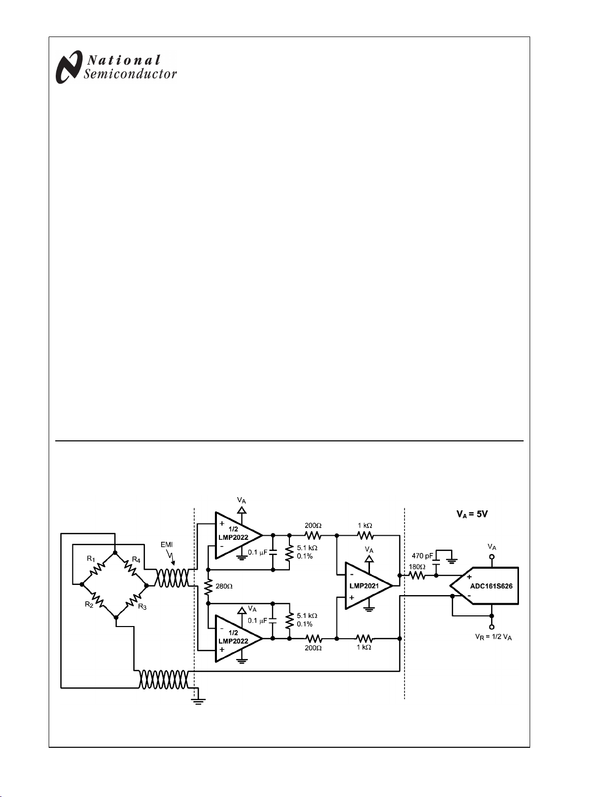
Typical Application
Bridge Amplifier
The LMP2021/LMP2022 support systems with up to 24 bits of accuracy.
LMP® is a registered trademark of National Semiconductor Corporation.
© 2008 National Semiconductor Corporation 300149 www.national.com
30014972
Page 2
Absolute Maximum Ratings (Note 1)
If Military/Aerospace specified devices are required,
please contact the National Semiconductor Sales Office/
Distributors for availability and specifications.
ESD Tolerance (Note 2)
Human Body Model 2000V
Machine Model 200V
LMP2021/LMP2022
Charge Device Model 1000V
VIN Differential ±V
Supply Voltage (VS = V+ – V−)
Output Short-Circuit Duration to V+ or V
(Note 3)
Storage Temperature Range −65°C to 150°C
−
6.0V
5s
Soldering Information
Infrared or Convection (20 sec) 235°C
Wave Soldering Lead Temperature
(10 sec) 260°C
Operating Ratings (Note 1)
Temperature Range −40°C to 125°C
Supply Voltage (VS = V+ – V–)
Package Thermal Resistance (θJA)
S
5-Pin SOT-23 164 °C/W
8-Pin SOIC (LMP2021) 106 °C/W
8-Pin SOIC (LMP2022) 106 °C/W
8-Pin MSOP 217 °C/W
Junction Temperature (Note 4) 150°C max
2.5V Electrical Characteristics (Note 5)
Unless otherwise specified, all limits are guaranteed for TA = 25°C, V+ = 2.5V, V− = 0V, VCM = V+/2, RL >10 kΩ to V+/2. Boldface limits apply at the temperature extremes.
Symbol Parameter Conditions Min
(Note 7)
V
OS
TCV
I
B
I
OS
CMRR Common Mode Rejection Ratio
CMVR Input Common-Mode Voltage Range
Input Offset Voltage –0.9 ±5
Input Offset Voltage Drift (Note 8) 0.001 ±0.02
OS
Input Bias Current ±23 ±100
Input Offset Current ±57 ±200
−0.2V ≤ VCM ≤ 1.7V
0V ≤ VCM ≤ 1.5V
Large Signal CMRR ≥ 105 dB
105
102
−0.2
Large Signal CMRR ≥ 102 dB
EMIRR Electro-Magnetic Interference
Rejection Ratio
(Note 9)
IN+
and
IN−
V
= 100 mVP (−20 dBVP)
RF-PEAK
f = 400 MHz
V
= 100 mVP (−20 dBVP)
RF-PEAK
f = 900 MHz
V
= 100 mVP (−20 dBVP)
RF-PEAK
f = 1800 MHz
V
= 100 mVP (−20 dBVP)
RF-PEAK
f = 2400 MHz
PSRR Power Supply Rejection Ratio
2.5V ≤ V+ ≤ 5.5V, VCM = 0
115
112
2.2V ≤ V+ ≤ 5.5V, VCM = 0
A
VOL
Large Signal Voltage Gain
RL = 10 kΩ to V+/2
V
= 0.5V to 2V
OUT
RL = 2 kΩ to V+/2
V
= 0.5V to 2V
OUT
110 130
124
119
120
115
0
40
48
67
79
Typ
(Note 6)
141
130
150
150
(Note 7)
2.2V to 5.5V
Max
±10
±300
±250
1.7
1.5
Units
μV
μV/°C
pA
pA
dB
V
dB
dB
dB
www.national.com 2
Page 3
LMP2021/LMP2022
Symbol Parameter Conditions Min
(Note 7)
V
OUT
Output Swing High
RL = 10 kΩ to V+/2
38 50
Typ
(Note 6)
Max
(Note 7)
Units
70
62 85
115
30 45
55
58 75
mV
from either
rail
Output Swing Low
RL = 2 kΩ to V+/2
RL = 10 kΩ to V+/2
RL = 2 kΩ to V+/2
95
I
OUT
I
S
SR Slew Rate (Note 10)
GBW Gain Bandwidth Product
G
M
Φ
M
C
IN
e
n
i
n
t
r
Linear Output Current Sourcing, V
Sinking, V
= 2V 30 50
OUT
= 0.5V 30 50
OUT
Supply Current Per Amplifier 0.95 1.10
1.37
2.5
5 MHz
10 dB
60 deg
Gain Margin
Phase Margin
AV = +1, CL = 20 pF, RL = 10 kΩ
VO = 2 V
PP
CL = 20 pF, RL = 10 kΩ
CL = 20 pF, RL = 10 kΩ
CL = 20 pF, RL = 10 kΩ
Input Capacitance Common Mode 12
Differential Mode 12
Input-Referred Voltage Noise
Density
f = 0.1 kHz or 10 kHz, AV = 1000 11
f = 0.1 kHz or 10 kHz, AV = 100 15
Input-Referred Voltage Noise 0.1 Hz to 10 Hz 260
0.01 Hz to 10 Hz 330
Input-Referred Current Noise f = 1 kHz 350
Recovery time
to 0.1%, RL = 10 kΩ, AV = −50,
V
= 1.25 VPP Step, Duration = 50 μs
OUT
50 µs
mA
mA
V/μs
pF
nV/
nV
fA/
CT Cross Talk LMP2022, f = 1 kHz 150 dB
PP
5V Electrical Characteristics (Note 5)
Unless otherwise specified, all limits are guaranteed for TA = 25°C, V+ = 5V, V− = 0V, VCM = V+/2, RL > 10 kΩ to V+/2. Boldface
limits apply at the temperature extremes.
Symbol Parameter Conditions Min
(Note 7)
V
OS
TCV
I
B
I
OS
CMRR Common Mode Rejection Ratio
CMVR Input Common-Mode Voltage Range
Input Offset Voltage −0.4 ±5
Input Offset Voltage Drift (Note 8) −0.004 ±0.02
OS
Input Bias Current ±25 ±100
Input Offset Current ±48 ±200
−0.2V ≤ VCM ≤ 4.2V
0V ≤ VCM ≤ 4.0V
Large Signal CMRR ≥ 120 dB
120
115
–0.2
Large Signal CMRR ≥ 115 dB
0
Typ
(Note 6)
139
4.2
Max
(Note 7)
±10
±300
±250
4.0
Units
μV
μV/°C
pA
pA
dB
V
3 www.national.com
Page 4
Symbol Parameter Conditions Min
EMIRR Electro-Magnetic Interference
Rejection Ratio
(Note 9)
LMP2021/LMP2022
IN+
and
IN−
V
= 100 mVP (−20 dBVP)
RF-PEAK
f = 400 MHz
V
= 100 mVP (−20 dBVP)
RF-PEAK
f = 900 MHz
V
= 100 mVP (−20 dBVP)
RF-PEAK
f = 1800 MHz
V
= 100 mVP (−20 dBVP)
RF-PEAK
(Note 7)
58
64
72
82
Typ
(Note 6)
Max
(Note 7)
f = 2400 MHz
PSRR Power Supply Rejection Ratio
2.5V ≤ V+ ≤ 5.5V, VCM = 0
115
130
112
2.2V ≤ V+ ≤ 5.5V, VCM = 0
A
VOL
Large Signal Voltage Gain
RL = 10 kΩ to V+/2
V
= 0.5V to 4.5V
OUT
RL = 2 kΩ to V+/2
V
= 0.5V to 4.5V
OUT
V
OUT
Output Swing High
RL = 10 kΩ to V+/2
110 130
125
160
120
123
160
118
83 135
170
RL = 2 kΩ to V+/2
120 160
204
Output Swing Low
RL = 10 kΩ to V+/2
65 80
105
RL = 2 kΩ to V+/2
103 125
158
I
OUT
I
S
Linear Output Current Sourcing, V
Sinking, V
= 4.5V 30 50
OUT
= 0.5V 30 50
OUT
Supply Current Per Amplifier 1.1 1.25
1.57
SR Slew Rate (Note 10)
GBW Gain Bandwidth Product
G
M
Φ
M
C
IN
Gain Margin
Phase Margin
Input Capacitance Common Mode 12
AV = +1, CL = 20 pF, RL = 10 kΩ
VO = 2 V
PP
CL = 20 pF, RL = 10 kΩ
CL = 20 pF, RL = 10 kΩ
CL = 20 pF, RL = 10 kΩ
2.6
5 MHz
10 dB
60 deg
Differential Mode 12
e
n
Input-Referred Voltage Noise Density f = 0.1 kHz or 10 kHz, AV= 1000 11
f = 0.1 kHz or 10 kHz, AV= 100 15
Input-Referred Voltage Noise 0.1 Hz to 10 Hz Noise 260
0.01 Hz to 10 Hz Noise 330
i
n
t
r
Input-Referred Current Noise f = 1 kHz 350
Input Overload Recovery time
to 0.1%, RL = 10 kΩ, AV = −50,
V
= 2.5 VPP Step, Duration = 50 μs
OUT
50
CT Cross Talk LMP2022, f = 1 kHz 150 dB
Units
dB
dB
dB
mV
from
either rail
mA
mA
V/μs
pF
nV/
nV
PP
fA/
μs
www.national.com 4
Page 5
Note 1: Absolute Maximum Ratings indicate limits beyond which damage to the device may occur. Operating Ratings indicate conditions for which the device is
intended to be functional, but specific performance is not guaranteed. For guaranteed specifications and the test conditions, see the Electrical Characteristics
Tables.
Note 2: Human Body Model per MIL-STD-883, Method 3015.7. Machine Model, per JESD22-A115-A. Field-Induced Charge-Device Model, per JESD22-C101C.
Note 3: Package power dissipation should be observed.
Note 4: The maximum power dissipation is a function of T
PD = (T
Note 5: Electrical Table values apply only for factory testing conditions at the temperature indicated. Factory testing conditions result in very limited self-heating
of the device such that TJ = TA. No guarantee of parametric performance is indicated in the electrical tables under conditions of internal self-heating where
TJ > TA.
Note 6: Typical values represent the most likely parametric norm at the time of characterization. Actual typical values may vary over time and will also depend
on the application and configuration. The typical values are not tested and are not guaranteed on shipped production material.
Note 7: All limits are guaranteed by testing, statistical analysis or design.
Note 8: Offset voltage temperature drift is determined by dividing the change in VOS at the temperature extremes by the total temperature change.
Note 9: The EMI Rejection Ratio is defined as EMIRR = 20Log ( V
Note 10: The number specified is the average of rising and falling slew rates and is measured at 90% to 10%.
- TA)/ θJA. All numbers apply for packages soldered directly onto a PC board.
J(MAX)
, θJA, and TA. The maximum allowable power dissipation at any ambient temperature is
J(MAX)
/ΔVOS).
R
F-PEAK
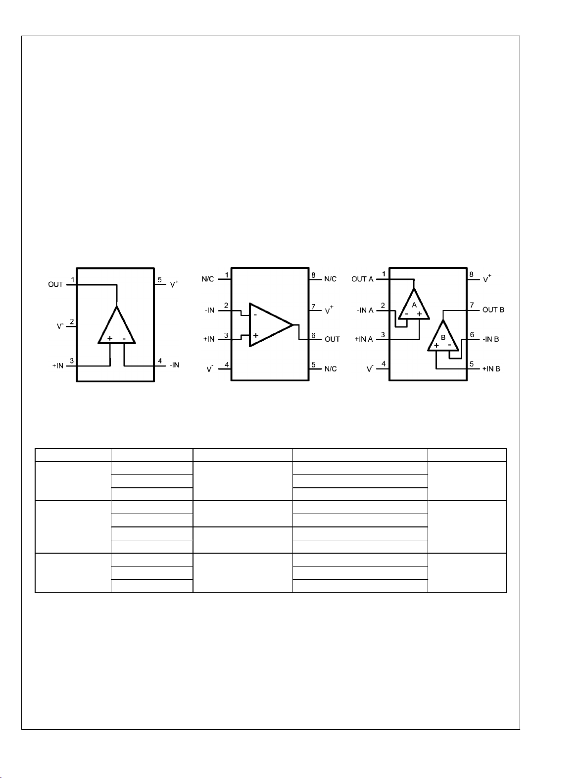
Connection Diagrams
LMP2021/LMP2022
5-Pin SOT-23
Top View
30014902
8-Pin SOIC (LMP2021)
Top View
8-Pin SOIC/MSOP (LMP2022)
30014953
Ordering Information
Package Part Number Package Marking Transport Media NSC Drawing
5-Pin SOT-23
8-Pin SOIC
8-Pin MSOP
LMP2021MF
AF5A
LMP2021MFX 3k Units Tape and Reel
LMP2021MA
LMP2021MAX 2.5k Units Tape and Reel
LMP2022MA
LMP2022MAX 2.5k Units Tape and Reel
LMP2021MA
LMP2022MA
LMP2022MM
AV5A
LMP2022MMX 3.5k Units Tape and Reel
1k Units Tape and Reel
95 Units/Rail
95 Units/Rail
1k Units Tape and Reel
30014903
MF05ALMP2021MFE 250 Units Tape and Reel
M08A
MUA08ALMP2022MME 250 Units Tape and Reel
5 www.national.com
Page 6
Typical Performance Characteristics Unless otherwise noted: T
VS= 5V, VCM = VS/2.
= 25°C, RL > 10 kΩ, VS= V+ – V–,
A
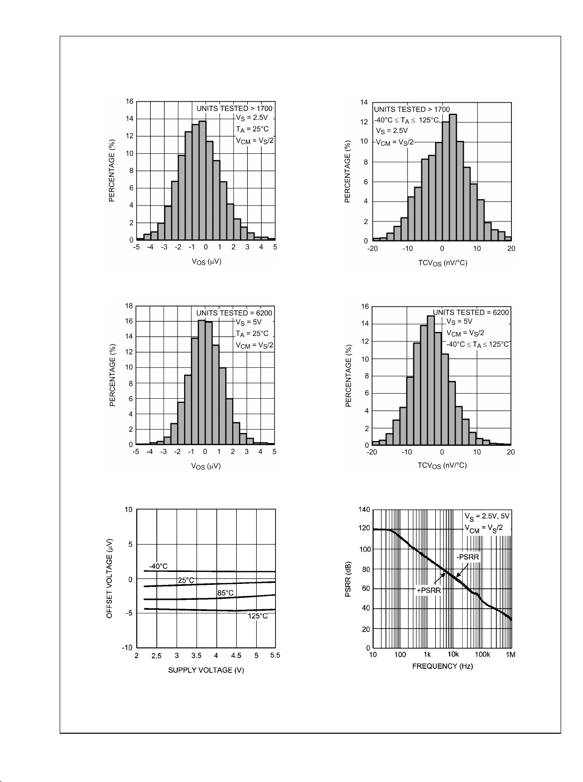
Offset Voltage Distribution
LMP2021/LMP2022
Offset Voltage Distribution
30014912
TCVOS Distribution
30014914
TCVOS Distribution
30014913
Offset Voltage vs. Supply Voltage
30014905
www.national.com 6
30014915
PSRR vs. Frequency
30014930
Page 7
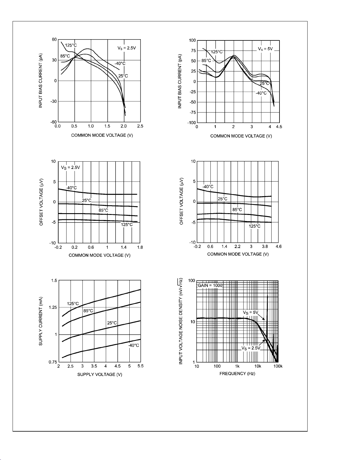
LMP2021/LMP2022
Input Bias Current vs. V
Offset Voltage vs. V
CM
CM
30014962
Input Bias Current vs. V
Offset Voltage vs. V
CM
30014961
CM
30014906
Supply Current vs. Supply Voltage (Per Amplifier)
30014904
30014907
Input Voltage Noise vs. Frequency
30014926
7 www.national.com
Page 8

Open Loop Frequency Response
LMP2021/LMP2022
Open Loop Frequency Response
30014922
Open Loop Frequency Response Over Temperature
30014923
EMIRR vs. Input Power
30014921
EMIRR vs. Frequency
30014934
EMIRR vs. Input Power
30014932
www.national.com 8
30014933
Page 9

LMP2021/LMP2022
Time Domain Input Voltage Noise
CMRR vs. Frequency
30014928
Time Domain Input Voltage Noise
30014929
Slew Rate vs. Supply Voltage
Output Swing High vs. Supply Voltage
30014931
30014909
30014916
Output Swing Low vs. Supply Voltage
30014911
9 www.national.com
Page 10

Output Swing High vs. Supply Voltage
LMP2021/LMP2022
Output Swing Low vs. Supply Voltage
Overload Recovery Time
Large Signal Step Response
30014908
30014942
30014910
Overload Recovery Time
30014943
Small Signal Step Response
30014920
www.national.com 10
30014918
Page 11

LMP2021/LMP2022
Large Signal Step Response
30014919
Output Voltage vs. Output Current
Small Signal Step Response
30014917
Cross Talk Rejection Ratio vs. Frequency (LMP2022)
30014924
30014973
11 www.national.com
Page 12

Application Information
LMP2021/LMP2022
The LMP2021/LMP2022 are single and dual precision operational amplifiers with ultra low offset voltage, ultra low offset
voltage drift, and very low input voltage noise with no 1/f and
extended supply voltage range. The LMP2021/LMP2022 offer on chip EMI suppression circuitry which greatly enhances
LMP2021/LMP2022
the performance of these precision amplifiers in the presence
of radio frequency signals and other disturbances.
The LMP2021/LMP2022 utilize proprietary techniques to
measure and continuously correct the input offset error voltage. The LMP2021/LMP2022 have a DC input offset voltage
with a maximum value of ±5 μV and an input offset voltage
drift maximum value of 0.02 µV/°C. The input voltage noise of
the LMP2021/LMP2022 is less than 11 nV/
gain of 1000 V/V and has no flicker noise component. This
makes the LMP2021/LMP2022 ideal for high accuracy, low
frequency applications where lots of amplification is needed
and the input signal has a very small amplitude.
The proprietary input offset correction circuitry enables the
LMP2021/LMP2022 to have superior CMRR and PSRR performances. The combination of an open loop voltage gain of
160 dB, CMRR of 142 dB, PSRR of 130 dB, along with the
ultra low input offset voltage of only −0.4 µV, input offset voltage drift of only −0.004 µV/°C, and input voltage noise of only
260 nV
great choices for high gain transducer amplifiers, ADC buffer
amplifiers, DAC I-V conversion, and other applications requiring precision and long-term stability. Other features are
rail-to-rail output, low supply current of 1.1 mA per amplifier,
and a gain-bandwidth product of 5 MHz.
The LMP2021/LMP2022 have an extended supply voltage
range of 2.2V to 5.5V, making them ideal for battery operated
portable applications. The LMP2021 is offered in 5-pin
SOT-23 and 8-pin SOIC packages. The LMP2022 is offered
in 8-pin MSOP and 8-Pin SOIC packages.
EMI SUPPRESSION
The near-ubiquity of cellular, bluetooth, and Wi-Fi signals and
the rapid rise of sensing systems incorporating wireless radios make electromagnetic interference (EMI) an evermore
important design consideration for precision signal paths.
Though RF signals lie outside the op amp band, RF carrier
switching can modulate the DC offset of the op amp. Also
some common RF modulation schemes can induce downconverted components. The added DC offset and the induced
signals are amplified with the signal of interest and thus corrupt the measurement. The LMP2021/LMP2022 use on chip
filters to reject these unwanted RF signals at the inputs and
power supply pins; thereby preserving the integrity of the precision signal path.
Twisted pair cabling and the active front-end’s common-mode
rejection provide immunity against low frequency noise (i.e.
60 Hz or 50 Hz mains) but are ineffective against RF interference. Figure 12 displays this. Even a few centimeters of PCB
trace and wiring for sensors located close to the amplifier can
pick up significant 1 GHz RF. The integrated EMI filters of
LMP2021/LMP2022 reduce or eliminate external shielding
and filtering requirements, thereby increasing system robustness. A larger EMIRR means more rejection of the RF interference. For more information on EMIRR, please refer to
AN-1698.
at 0.1 Hz to 10 Hz make the LMP2021/LMP2022
PP
at a voltage
INPUT VOLTAGE NOISE
The input voltage noise density of the LMP2021/LMP2022
has no 1/f corner, and its value depends on the feedback network used. This feature of the LMP2021/LMP2022 differentiates this family from other products currently available from
other vendors. In particular, the input voltage noise density
decreases as the closed loop voltage gain of the LMP2021/
LMP2022 increases. The input voltage noise of the LMP2021/
LMP2022 is less than 11 nV/
when the closed loop voltage gain of the op amp is 1000. Higher voltage gains are
required for smaller input signals. When the input signal is
smaller, a lower input voltage noise is quite advantageous
and increases the signal to noise ratio.
Figure 1 shows the input voltage noise of the LMP2021/
LMP2022 as the closed loop gain increases.
30014959
FIGURE 1. Input Voltage Noise Density decreases with
Gain
Figure 2 shows the input voltage noise density does not have
the 1/f component.
30014951
FIGURE 2. Input Voltage Noise Density with no 1/f
With smaller and smaller input signals and high precision applications with lower error budget, the reduced input voltage
noise and no 1/f noise allow more flexibility in circuit design.
www.national.com 12
Page 13

ACHIEVING LOWER NOISE WITH FILTERING
The low input voltage noise of the LMP2021/LMP2022, and
no 1/f noise make these suitable for many applications with
noise sensitive designs. Simple filtering can be done on the
LMP2021/LMP2022 to remove high frequency noise. Figure
3 shows a simple circuit that achieves this.
In Figure 3 CF and the corner frequency of the filter resulting
from CF and RF will reduce the total noise.
30014936
FIGURE 3. Noise Reducing Filter for Lower Gains
In order to achieve lower noise floors for even more noise
stringent applications, a simple filter can be added to the op
amp’s output after the amplification stage. Figure 4 shows the
schematic of a simple circuit which achieves this objective.
Low noise amplifiers such as the LMV771 can be used to
create a single pole low pass filter on the output of the
LMP2021/LMP2022. The noise performance of the filtering
amplifier, LMV771 in this circuit, will not be dominant as the
input signal on LMP2021/LMP2022 has already been significantly gained up and as a result the effect of the input voltage
noise of the LMV771 is effectively not noticeable.
30014956
FIGURE 4. Enhanced Filter to Further Reduce Noise at
Higher Gains
Using the circuit in Figure 4 has the advantage of removing
the non-linear filter bandwidth dependency which is seen
when the circuit in Figure 3 is used. The difference in noise
performance of the circuits in Figures 3, 4 becomes apparent
only at higher gains. At voltage gains of 10 V/V or less, there
is no difference between the noise performance of the two
circuits.
30014974
FIGURE 5. RMS Input Referred Noise vs. Frequency
Figure 5 shows the total input referred noise vs. 3 dB corner
of both filters of Figure 3 and Figure 4 at gains of 100V/V and
1000V/V. For these measurements and using Figure 3's cir-
cuit, RF = 49.7 kΩ and RIN = 497Ω. Value of CF has been
changed to achieve the desired 3 dB filter corner frequency.
In the case of Figure 4's circuit, RF = 49.7 kΩ and RIN =
497Ω, R
achieve the desired 3 dB filter corner frequency. Figure 5
= 49.7 kΩ, and C
FILT
has been changed to
FILT
compares the RMS noise of these two circuits. As Figure 5
shows, the RMS noise measured the circuit in Figure 4 has
lower values and also depicts a more linear shape.
DIGITAL ACQUISITION SYSTEMS
High resolution ADC’s with 16-bits to 24-bits of resolution can
be limited by the noise of the amplifier driving them. The circuit
configuration, the value of the resistors used and the source
impedance seen by the amplifier can affect the noise of the
amplifier. The total noise at the output of the amplifier can be
dominated by one of several sources of noises such as: white
noise or broad band noise, 1/f noise, thermal noise, and current noise. In low frequency applications such as medical
instrumentation, the source impedance is generally low
enough that the current noise coupled into it does not impact
the total noise significantly. However, as the 1/f or flicker noise
is paramount to many application, the use of an auto correcting stabilized amplifier like the LMP2021/LMP2022 reduces
the total noise.
Table 1: RMS Input Noise Performance summarizes the input
and output referred RMS noise values for the LMP2021/
LMP2022 compared to that of Competitor A. As described in
previous sections, the outstanding noise performance of the
LMP2021/LMP2022 can be even further improved by adding
a simple low pass filter following the amplification stage.
The use of an additional filter, as shown in Figure 4 benefits
applications with higher gain. For this reason, at a gain of 10,
only the results of circuit in Figure 3 are shown. The RMS
input noise of the LMP2021/LMP2022 are compared with
Competitor A's input noise performance. Competitor A's RMS
input noise behaves the same with or without an additional
filter.
LMP2021/LMP2022
13 www.national.com
Page 14

Table 1: RMS Input Noise Performance
Amplifier
Gain
(V/V)
LMP2021/LMP2022
10
100
System
Bandwidth
Requirement
(Hz)
100 229 * 300
1000 763 * 1030
100 229 196 300
1000 763 621 1030
RMS Input Noise (nV)
LMP2021/LMP2022
Figure 3
Circuit
Figure 4
Circuit
10 71 46 95
1000
100 158 146 300
1000 608 462 1030
* No significant difference in Noise measurements at
AV = 10V/V
INPUT BIAS CURRENT
The bias current of the LMP2021/LMP2022 behaves differently than a conventional amplifier due to the dynamic tran-
Competitor
A
Figures 4, 3
Circuit
sient currents created on the input of an auto-zero circuit. The
input bias current is affected by the charge and discharge
current of the input auto-zero circuit. The amount of current
sunk or sourced from that stage is dependent on the combination of input impedance (resistance and capacitance), as
well as the balance and matching of these impedances across
the two inputs. This current, integrated in the auto-zero circuit,
causes a shift in the apparent "bias current". Because of this,
there is an apparent "bias current vs. input impedance" interaction. In the LMP2021/LMP2022 for an input resistive
impedance of 1 GΩ, the shift in input bias current can be up
to 40 pA. This input bias shift is caused by varying the input's
capacitive impedance. Since the input bias current is dependent on the input impedance, it is difficult to estimate what the
actual bias current is without knowing the end circuit and associated capacitive strays.
Figure 6 shows the input bias current of the LMP2021/
LMP2022 and that of another commercially available amplifier from a competitor. As it can be seen, the shift in LMP2021/
LMP2022 bias current is much lower than that of other chopper style or auto zero amplifiers available from other vendors.
FIGURE 6. Input Bias Current of LMP2021/LMP2022 is lower than Competitor A
LOWERING THE INPUT BIAS CURRENT
As mentioned in the INPUT BIAS CURRENT section, the input bias current of an auto zero amplifier such as the
LMP2021/LMP2022 varies with input impedance and feedback impedance. Once the value of a certain input resistance,
i.e. sensor resistance, is known, it is possible to optimize the
input bias current for this fixed input resistance by choosing
the capacitance value that minimizes that current. Figure 7
shows the input bias current vs. input impedance of the
LMP2021/LMP2022. The value of RG or input resistance in
this test is 1 GΩ. When this value of input resistance is used,
and when a parallel capacitance of 22 pF is placed on the
circuit, the resulting input bias current is nearly 0 pA.
Figure 7 can be used to extrapolate capacitor values for other
sensor resistances. For this purpose, the total impedance
seen by the input of the LMP2021/LMP2022 needs to be calculated based on Figure 7. By knowing the value of RG, one
can calculate the corresponding CG which minimizes the noninverting input bias current, positive bias current, value.
www.national.com 14
30014975
30014964
FIGURE 7. Input Bias Current vs. CG with RG = 1 GΩ
Page 15

LMP2021/LMP2022
In a typical I-V converter, the output voltage will be the sum
of DC offset plus bias current and the applied signal through
the feedback resistor. In a conventional input stage, the inverting input's capacitance has very little effect on the circuit.
This effect is generally on settling time and the dielectric
soakage time and can be ignored. In auto zero amplifiers, the
input capacitance effect will add another term to the output.
This additional term means that the baseline reading on the
output will be dependent on the input capacitance. The term
input capacitance for this purpose includes circuit strays and
any input cable capacitances. There is a slight variation in the
capacitive offset as the duty cycle and amplitude of the pulses
vary from part to part, depending on the correction at the time.
The lowest input current will be obtained when the
impedances, both resistive and capacitive, are matched between the inputs. By balancing the input capacitances, the
effect can be minimized. A simple way to balance the input
impedance is adding a capacitance in parallel to the feedback
resistance. The addition of this feedback capacitance reduces the bias current and increases the stability of the
operational amplifier. Figure 8 shows the input bias current of
the LMP2021/LMP2022 when RF is set to 1 GΩ. As it can be
seen from Figure 8, choosing the optimum value of CF will
help reducing the input bias current.
SENSOR IMPEDANCE
The sensor resistance, or the resistance connected to the inputs of the LMP2021/LMP2022, contributes to the total
impedance seen by the auto correcting input stage.
30014967
30014968
FIGURE 9. AUTO CORRECTING INPUT STAGE MODEL
As shown in Figure 9, the sum of RIN and R
a low pass filter with C
increases, the time constant of this filter increases, resulting
during correction cycles. As R
OUT
ON-SWITCH
will form
in a slower output signal which could have the effect of reducing the open loop gain, A
In order to prevent this reduction in A
impedance sensors or other high resistances connected to
, of the LMP2021/LMP2022.
VOL
in presence of high
VOL
the input of the LMP2021/LMP2022, a capacitor can be
placed in parallel to this input resistance. This is shown in
Figure 10
IN
30014965
FIGURE 8. Input Bias Current vs. CF with RF = 1 GΩ
The effect of bias current on a circuit can be estimated with
the following:
AV*I
Where AV is the closed loop gain of the system and I
I
denote the positive and negative bias current, respec-
BIAS−
tively. It is common to show the average of these bias currents
in product datasheets. If I
specified, use the I
tables for this calculation.
value provided in datasheet graphs or
BIAS
BIAS+*ZS
BIAS+
- I
BIAS−*ZF
and I
are not individually
BIAS−
BIAS+
and
For the application circuit shown in Figure 12, the LMP2022
amplifiers each have a gain of 18. With a sensor impedance
of 500Ω for the bridge, and using the above equation, the total
error due to the bias current on the outputs of the LMP2022
amplifier will be less than 200 nV.
30014969
30014970
FIGURE 10. Sensor Impedance with Parallel Capacitance
15 www.national.com
Page 16

CIN in Figure 10 adds a zero to the low pass filter and hence
eliminating the reduction in A
An alternative circuit to achieve this is shown in Figure 11.
of the LMP2021/LMP2022.
VOL
LMP2021/LMP2022
FIGURE 11. Alternative Sensor Impedance Circuit
TRANSIENT RESPONSE TO FAST INPUTS
On chip continuous auto zero correction circuitry eliminates
the 1/f noise and significantly reduces the offset voltage and
offset voltage drift; all of which are very low frequency events.
For slow changing sensor signals this correction is transparent. For excitations which may otherwise cause the output to
swing faster than 40 mV/µs, there are additional considerations which can be viewed two perspectives: for sine waves
and for steps.
For sinusoidal inputs, when the output is swinging rail-to-rail
on ±2.5V supplies, the auto zero circuitry will introduce distortions above 2.55 kHz. For smaller output swings, higher
frequencies can be amplified without the auto zero slew limitation as shown in table below. Signals above 20 kHz, are not
affected, though normally, closed loop bandwidth should be
kept below 20 kHz so as to avoid aliasing from the auto zero
circuit.
V
OUT-PEAK
For step-like inputs, such as those arising from disturbances
to a sensing system, the auto zero slew rate limitation manifests itself as an extended ramping and settling time, lasting
~100 µs.
DIFFERENTIAL BRIDGE SENSOR
Bridge sensors are used in a variety of applications such as
pressure sensors and weigh scales. Bridge sensors typically
have a very small differential output signal. This very small
signal needs to be accurately amplified before it can be fed
into an ADC. As discussed in the previous sections, the accuracy of the op amp used as the ADC driver is essential to
maintaining total system accuracy.
The high DC performance of the LMP2021/LMP2022 make
these amplifiers ideal choices for use with a bridge sensor.
The LMP2021/LMP2022 have very low input offset voltage
and very low input offset voltage drift. The open loop gain of
the LMP2021/LMP2022 is 160 dB.
(V) f
MAX-SINE WAVE
0.32 20
1 6.3
2.5 2.5
(kHz)
30014971
The on chip EMI rejection filters available on the LMP2021/
LMP2022 help remove the EMI interference introduced to the
signal and hence improve the overall system performance.
The circuit in Figure 12 shows a signal path solution for a typical bridge sensor using the LMP2021/LMP2022. Bridge sensors are created by replacing at least one, and up to all four,
of the resistors in a typical bridge with a sensor whose resistance varies in response to an external stimulus. Using four
sensors has the advantage of increasing output dynamic
range. Typical output voltage of one resistive pressure sensor
is 2 mV per 1V of bridge excitation voltage. Using four sensors, the output of the bridge is 8 mV per 1V. The bridge
voltage is this system is chosen to be 1/2 of the analog supply
voltage and equal to the reference voltage of the ADC161S626, 2.5V. This excitation voltage results in 2.5V * 8
mV = 20 mV of differential output signal on the bridge. This
20 mV signal must be accurately amplified by the amplifier to
best match the dynamic input range of the ADC. This is done
by using one LMP2022 and one LMP2021 in front of the ADC161S626. The gaining of this 20 mV signal is achieved in 2
stages and through an instrumentation amplifier. The
LMP2022 in Figure 12 amplifies each side of the differential
output of the bridge sensor by a gain 18. Bridge sensor measurements are usually done up to 10s of Hz. Placing a
300 Hz filter on the LMP2022 helps removing the higher frequency noise from this circuit. This filter is created by placing
two capacitors in the feedback path of the LMP2022 amplifiers. Using the LMP2022 with a gain of 18 reduces the input
referred voltage noise of the op amps and the system as a
result. Also, this gain allows direct filtering of the signal on the
LMP2022 without compromising noise performance. The differential output of the two amplifiers in the LMP2022 are then
fed into a LMP2021 configured as a difference amplifier. This
stage has a gain of 5, with a total system having a gain of
(18*2+1)*5 = 185. The LMP2021 has an outstanding CMRR
value of 139. This impressive CMRR improves system performance by removing the common mode signal introduced
by the bridge. With an overall gain of 185, the 20 mV differential input signal is gained up to 3.7V. This utilizes the
amplifiers output swing as well as the ADC's input dynamic
range.
This amplified signal is then fed into the ADC161S626. The
ADC161S626 is a 16-bit, 50 kSPS to 250 kSPS 5V ADC. In
order to utilize the maximum number of bits of the ADC161S626 in this configuration, a 2.5V reference voltage is
used. This 2.5V reference is also used to power the bridge
sensor and the inverting input of the ADC. Using the same
voltage source for these three points helps reducing the total
system error by eliminating error due to source variations.
With this system, the output signal of the bridge sensor which
can be up to 20 mV is accurately gained to the full scale of
the ADC and then digitized for further processing. The
LMP2021/LMP2022 introduced minimal error to the system
and improved the signal quality by removing common model
signals and high frequency noise.
www.national.com 16
Page 17

FIGURE 12. LMP2021/LMP2022 used with ADC161S626
LMP2021/LMP2022
30014972
17 www.national.com
Page 18

Physical Dimensions inches (millimeters) unless otherwise noted
LMP2021/LMP2022
5-Pin SOT-23
NS Package Number MF05A
NS Package Number M08A
www.national.com 18
8-Pin SOIC
Page 19

LMP2021/LMP2022
NS Package Number MUA08A
8-Pin MSOP
19 www.national.com
Page 20

Notes
For more National Semiconductor product information and proven design tools, visit the following Web sites at:
Products Design Support
Amplifiers www.national.com/amplifiers WEBENCH® Tools www.national.com/webench
Audio www.national.com/audio App Notes www.national.com/appnotes
Clock and Timing www.national.com/timing Reference Designs www.national.com/refdesigns
Data Converters www.national.com/adc Samples www.national.com/samples
Interface www.national.com/interface Eval Boards www.national.com/evalboards
LVDS www.national.com/lvds Packaging www.national.com/packaging
Power Management www.national.com/power Green Compliance www.national.com/quality/green
Switching Regulators www.national.com/switchers Distributors www.national.com/contacts
LDOs www.national.com/ldo Quality and Reliability www.national.com/quality
LED Lighting www.national.com/led Feedback/Support www.national.com/feedback
Voltage Reference www.national.com/vref Design Made Easy www.national.com/easy
PowerWise® Solutions www.national.com/powerwise Solutions www.national.com/solutions
Serial Digital Interface (SDI) www.national.com/sdi Mil/Aero www.national.com/milaero
Temperature Sensors www.national.com/tempsensors Solar Magic® www.national.com/solarmagic
Wireless (PLL/VCO) www.national.com/wireless Analog University® www.national.com/AU
THE CONTENTS OF THIS DOCUMENT ARE PROVIDED IN CONNECTION WITH NATIONAL SEMICONDUCTOR CORPORATION
(“NATIONAL”) PRODUCTS. NATIONAL MAKES NO REPRESENTATIONS OR WARRANTIES WITH RESPECT TO THE ACCURACY
OR COMPLETENESS OF THE CONTENTS OF THIS PUBLICATION AND RESERVES THE RIGHT TO MAKE CHANGES TO
SPECIFICATIONS AND PRODUCT DESCRIPTIONS AT ANY TIME WITHOUT NOTICE. NO LICENSE, WHETHER EXPRESS,
IMPLIED, ARISING BY ESTOPPEL OR OTHERWISE, TO ANY INTELLECTUAL PROPERTY RIGHTS IS GRANTED BY THIS
DOCUMENT.
TESTING AND OTHER QUALITY CONTROLS ARE USED TO THE EXTENT NATIONAL DEEMS NECESSARY TO SUPPORT
NATIONAL’S PRODUCT WARRANTY. EXCEPT WHERE MANDATED BY GOVERNMENT REQUIREMENTS, TESTING OF ALL
PARAMETERS OF EACH PRODUCT IS NOT NECESSARILY PERFORMED. NATIONAL ASSUMES NO LIABILITY FOR
APPLICATIONS ASSISTANCE OR BUYER PRODUCT DESIGN. BUYERS ARE RESPONSIBLE FOR THEIR PRODUCTS AND
APPLICATIONS USING NATIONAL COMPONENTS. PRIOR TO USING OR DISTRIBUTING ANY PRODUCTS THAT INCLUDE
NATIONAL COMPONENTS, BUYERS SHOULD PROVIDE ADEQUATE DESIGN, TESTING AND OPERATING SAFEGUARDS.
EXCEPT AS PROVIDED IN NATIONAL’S TERMS AND CONDITIONS OF SALE FOR SUCH PRODUCTS, NATIONAL ASSUMES NO
LIABILITY WHATSOEVER, AND NATIONAL DISCLAIMS ANY EXPRESS OR IMPLIED WARRANTY RELATING TO THE SALE
AND/OR USE OF NATIONAL PRODUCTS INCLUDING LIABILITY OR WARRANTIES RELATING TO FITNESS FOR A PARTICULAR
LMP2021/LMP2022 Zero Drift, Low Noise, EMI Hardened Amplifiers
PURPOSE, MERCHANTABILITY, OR INFRINGEMENT OF ANY PATENT, COPYRIGHT OR OTHER INTELLECTUAL PROPERTY
RIGHT.
LIFE SUPPORT POLICY
NATIONAL’S PRODUCTS ARE NOT AUTHORIZED FOR USE AS CRITICAL COMPONENTS IN LIFE SUPPORT DEVICES OR
SYSTEMS WITHOUT THE EXPRESS PRIOR WRITTEN APPROVAL OF THE CHIEF EXECUTIVE OFFICER AND GENERAL
COUNSEL OF NATIONAL SEMICONDUCTOR CORPORATION. As used herein:
Life support devices or systems are devices which (a) are intended for surgical implant into the body, or (b) support or sustain life and
whose failure to perform when properly used in accordance with instructions for use provided in the labeling can be reasonably expected
to result in a significant injury to the user. A critical component is any component in a life support device or system whose failure to perform
can be reasonably expected to cause the failure of the life support device or system or to affect its safety or effectiveness.
National Semiconductor and the National Semiconductor logo are registered trademarks of National Semiconductor Corporation. All other
brand or product names may be trademarks or registered trademarks of their respective holders.
Copyright© 2008 National Semiconductor Corporation
For the most current product information visit us at www.national.com
www.national.com
National Semiconductor
Americas Technical
Support Center
Email: support@nsc.com
Tel: 1-800-272-9959
National Semiconductor Europe
Technical Support Center
Email: europe.support@nsc.com
German Tel: +49 (0) 180 5010 771
English Tel: +44 (0) 870 850 4288
National Semiconductor Asia
Pacific Technical Support Center
Email: ap.support@nsc.com
National Semiconductor Japan
Technical Support Center
Email: jpn.feedback@nsc.com
Page 21

 Loading...