

Page 1
March 6, 2008
LMK01000/LMK01010/LMK01020
1.6 GHz High Performance Clock Buffer, Divider, and
Distributor
General Description
The LMK01000/LMK01010/LMK01020 family provides an
easy way to divide and distribute high performance clock signals throughout the system. These devices provide best-inclass noise performance and are designed to be pin-to-pin
and footprint compatible with LMK03000/LMK02000 family of
precision clock conditioners.
The LMK01000/LMK01010/LMK01020 family features two
programmable clock inputs (CLKin0 and CLKin1) that allow
the user to dynamically switch between different clock domains.
Each device features 8 clock outputs with independently programmable dividers and delay adjustments. The outputs of
the device can be easily synchronized by an external pin
(SYNC*).
Target Applications
■
High performance Clock Distribution
■
Wireless Infrastructure
■
Medical Imaging
■
Wired Communications
■
Test and Measurement
■
Military / Aerospace
Features
■
30 fs additive jitter (100 Hz to 20 MHz)
■
Dual clock inputs
■
Programmable output channels (0 to 1600 MHz)
—
LMK01000: 3 LVDS outputs (CLKout0 - CLKout2) + 5
LVPECL outputs (CLKout3 - CLKout7)
—
LMK01010: 8 LVDS outputs
—
LMK01020: 8 LVPECL outputs
—
Channel divider values of 1, 2 to 510 (even divides)
—
Programmable output skew control
■
External synchronization
■
Pin compatible family of clocking devices
■
3.15 to 3.45 V operation
■
Package: 48 pin LLP (7.0 x 7.0 x 0.8 mm)
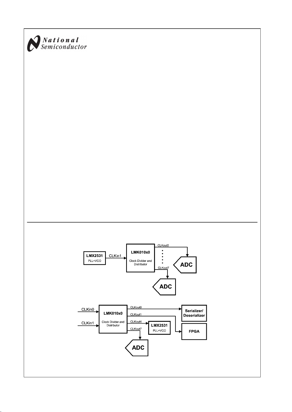
System Diagram
30042806
TRI-STATE® is a registered trademark of National Semiconductor Corporation.
© 2008 National Semiconductor Corporation 300428 www.national.com
LMK01000/LMK01010/LMK01020 1.6 GHz High Performance Clock Buffer, Divider, and
Distributor
Page 2
Functional Block Diagram
30042801
Connection Diagram
48-Pin LLP Package
30042802
www.national.com 2
LMK01000/LMK01010/LMK01020
Page 3
Pin Descriptions
Pin # Pin Name I/O Description
1, 25 GND - Ground
2, 7, 9,10, 32 NC - No Connect. Pin is not connected to the die.
3, 8, 13, 16, 19, 22, 26,
30, 31, 33, 37, 40, 43, 46
Vcc1, Vcc2, Vcc3, Vcc4, Vcc5, Vcc6, Vcc7,
Vcc8, Vcc9, Vcc10, Vcc11, Vcc12, Vcc13, Vcc14
- Power Supply
4 CLKuWire I MICROWIRE Clock Input
5 DATAuWire I MICROWIRE Data Input
6 LEuWire I MICROWIRE Latch Enable Input
11 GOE I Global Output Enable
12 Test O
This is an output pin used strictly for test purposes
and should be not connected for normal operation.
However, any load of an impedance of more than 1
kΩ is acceptable.
14, 15 CLKout0, CLKout0* O Clock Output 0
17, 18 CLKout1, CLKout1* O Clock Output 1
20, 21 CLKout2, CLKout2* O Clock Output 2
23, 24 CLKout3, CLKout3* O Clock Output 3
27 SYNC* I Global Clock Output Synchronization
28, 29 CLKin0,CLKin0* I CLKin 0 Input; Must be AC coupled
34, 35 CLKin1, CLKin1* I CLKin 1 Input; Must be AC coupled
36 Bias I Bias Bypass
38, 39 CLKout4, CLKout4* O Clock Output 4
41, 42 CLKout5, CLKout5* O Clock Output 5
44, 45 CLKout6, CLKout6* O Clock Output 6
47, 48 CLKout7, CLKout7* O Clock Output 7
DAP DAP - Die Attach Pad should be connected to ground.
The LMK01000 family is footprint compatible with the LMK03000/02000 family of devices. All CLKout pins are pin-to-pin compatible,
and CLKin0 and CLKin1 are equivalent to OSCin and Fin, respectively .
3 www.national.com
LMK01000/LMK01010/LMK01020
Page 4
Absolute Maximum Ratings (Notes 1, 2)
If Military/Aerospace specified devices are required, please contact the National Semiconductor Sales Office/ Distributors
for availability and specifications.
Parameter Symbol Ratings Units
Power Supply Voltage
V
CC
-0.3 to 3.6 V
Input Voltage
V
IN
-0.3 to (VCC + 0.3)
V
Storage Temperature Range
T
STG
-65 to 150 °C
Lead Temperature (solder 4 s)
T
L
+260 °C
Junction Temperature
T
J
125 °C
Recommended Operating Conditions
Parameter Symbol Min Typ Max Units
Ambient Temperature
T
A
-40 25 85 °C
Power Supply Voltage
V
CC
3.15 3.3 3.45 V
Note 1: "Absolute Maximum Ratings" indicate limits beyond which damage to the device may occur, including inoperability and degradation of device reliability
and/or performance. Functional operation of the device and/or non-degradation at the Absolute Maximum Ratings or other conditions beyond those indicated in
the Recommended Operating Conditions is not implied. The Recommended Operating Conditions indicate conditions at which the device is functional and the
device should not be operated beyond such conditions.
Note 2: This device is a high performance integrated circuit with ESD handling precautions. Handling of this device should only be done at ESD protected work
stations. The device is rated to a HBM-ESD of > 2 kV, a MM-ESD of > 200 V, and a CDM-ESD of > 1.2 kV.
Package Thermal Resistance
Package
θ
JA
θ
J-PAD (Thermal Pad)
48-Lead LLP (Note 3) 27.4° C/W 5.8° C/W
Note 3: Specification assumes 16 thermal vias connect the die attach pad to the embedded copper plane on the 4-layer JEDEC board. These vias play a key
role in improving the thermal performance of the LLP. It is recommended that the maximum number of vias be used in the board layout.
Electrical Characteristics (Note 4)
(3.15 V ≤ Vcc ≤ 3.45 V, -40 °C ≤ TA ≤ 85 °C, Differential Inputs/Outputs; except as specified. Typical values represent most likely
parametric norms at Vcc = 3.3 V, TA = 25 °C, and at the Recommended Operation Conditions at the time of product characterization
and are not guaranteed).
Symbol Parameter Conditions Min Typ Max Units
Current Consumption
I
CC
Power Supply Current
(Note 5)
All outputs
enabled, no
divide or delay
( CLKoutX_MUX
= Bypassed )
LMK01000 271
mA
LMK01010 160
LMK01020 338
Per channel, no
divide or delay
(CLKoutX_MUX
= Bypassed )
LVDS 17.8
LVPECL
(Includes Emitter
Resistors)
40
ICCPD
Power Down Current POWERDOWN = 1 1
CLKin0, CLKin0*, CLKin1, CLKin1*
f
CLKin
CLKin Frequency Range 1 1600 MHz
SLEW
CLKin
CLKin Frequency Input Slew Rate (Notes 6, 8) 0.5 V/ns
DUTY
CLKin
CLKin Frequency Input Duty Cycle
f
CLKin
≤ 800 MHz
30 70
%
f
CLKin
> 800 MHz
40 60
P
CLKin
Input Power Range for CLKin or
CLKin*
AC coupled -13 5 dBm
www.national.com 4
LMK01000/LMK01010/LMK01020
Page 5
Symbol Parameter Conditions Min Typ Max Units
Clock Distribution Section--Delays
Delay
CLKout
Maximum Allowable Delay(Note 8)
f
CLKoutX
≤ 1 GHz
(Delay is limited to maximum
programmable value)
2250
ps
f
CLKoutX
> 1 GHz
(Delay is limited to 1/2 of a period)
0.5/
f
CLKoutX
Clock Distribution Section - Divides
Divide
CLKoutX
Allowable divide range. (Note that 1 is
the only allowable odd divide value)
f
CLKinX
≤ 1300 MHz
1 510
n/a
1300 MHz < f
CLKinX
≤ 1600 MHz
1 2
Clock Distribution Section - LVDS Clock Outputs
Jitter
ADD
Additive RMS Jitter (Note 7)
RL = 100 Ω
Bandwidth =
100 Hz to 20 MHz
Vboost = 1
f
CLKoutX
= 200 MHz
80
fs
f
CLKoutX
= 800 MHz
30
f
CLKoutX
= 1600 MHz
25
Noise Floor Divider Noise Floor(Note 7)
RL = 100
Vboost = 1
f
CLKoutX
= 200 MHz
-156
dBc/Hz
f
CLKoutX
= 800 MHz
-153
f
CLKoutX
= 1600 MHz
-148
t
SKEW
CLKoutX to CLKoutY (Note 8)
Equal loading and identical clock
configuration
RL = 100 Ω
-30 ±4 30 ps
V
OD
Differential Output Voltage (Note 9)
Vboost=0 250 350 450
mV
Vboost=1 390
ΔV
OD
Change in magnitude of VOD for
complementary output states
RL = 100 Ω
-50 50 mV
V
OS
Output Offset Voltage
RL = 100 Ω
1.070 1.25 1.370 V
ΔV
OS
Change in magnitude of VOS for
complementary output states
RL = 100 Ω
-35 35 mV
I
SA
I
SB
Clock Output Short Circuit Current
single ended
Single ended outputs shorted to GND -24 24 mA
I
SAB
Clock Output Short Circuit Current
differential
Complementary outputs tied together -12 12 mA
5 www.national.com
LMK01000/LMK01010/LMK01020
Page 6
Symbol Parameter Conditions Min Typ Max Units
Clock Distribution Section - LVPECL Clock Outputs
Jitter
ADD
Additive RMS Jitter(Note 7)
RL = 100 Ω
Bandwidth =
100 Hz to 20 MHz
Vboost = 1
f
CLKoutX
= 200 MHz
65
fs
f
CLKoutX
= 800 MHz
25
f
CLKoutX
= 1600 MHz
25
Noise Floor Divider Noise Floor(Note 7)
RL = 100
Vboost = 1
f
CLKoutX
= 200 MHz
-158
dBc/Hz
f
CLKoutX
= 800 MHz
-154
f
CLKoutX
= 1600 MHz
-148
t
SKEW
CLKoutX to CLKoutY (Note 8)
Equal loading and identical clock
configuration
Termination = 50 Ω to Vcc - 2 V
-30 ±3 30 ps
V
OH
Output High Voltage
Termination = 50 Ω to Vcc - 2 V
Vcc -
0.98
V
V
OL
Output Low Voltage
Vcc -
1.8
V
V
OD
Differential Output Voltage (Note 9)
Vboost = 0 660 810 965
mV
Vboost = 1 865
Digital LVTTL Interfaces (Note 10)
V
IH
High-Level Input Voltage 2.0 Vcc V
V
IL
Low-Level Input Voltage 0.8 V
I
IH
High-Level Input Current
VIH = Vcc
-5.0 5.0 µA
I
IL
Low-Level Input Current
VIL = 0
-40.0 5.0 µA
V
OH
High-Level Output Voltage
IOH = +500 µA
Vcc -
0.4
V
V
OL
Low-Level Output Voltage
IOL = -500 µA
0.4 V
www.national.com 6
LMK01000/LMK01010/LMK01020
Page 7

Symbol Parameter Conditions Min Typ Max Units
Digital MICROWIRE Interfaces (Note 11)
V
IH
High-Level Input Voltage 1.6 Vcc V
V
IL
Low-Level Input Voltage 0.4 V
I
IH
High-Level Input Current
VIH = Vcc
-5.0 5.0 µA
I
IL
Low-Level Input Current
VIL = 0
-5.0 5.0 µA
MICROWIRE Timing
t
CS
Data to Clock Set Up Time See Data Input Timing 25 ns
t
CH
Data to Clock Hold Time See Data Input Timing 8 ns
t
CWH
Clock Pulse Width High See Data Input Timing 25 ns
t
CWL
Clock Pulse Width Low See Data Input Timing 25 ns
t
ES
Clock to Enable Set Up Time See Data Input Timing 25 ns
t
CES
Enable to Clock Set Up Time See Data Input Timing 25 ns
t
EWH
Enable Pulse Width High See Data Input Timing 25 ns
Note 4: The Electrical Characteristics tables list guaranteed specifications under the listed Recommended Operating Conditions except as otherwise modified
or specified by the Electrical Characteristics Conditions and/or Notes. Typical specifications are estimations only and are not guaranteed.
Note 5: See section 3.2 for more current consumption / power dissipation calculation information.
Note 6: For all frequencies the slew rate, SLEW
CLKin1
, is measured between 20% and 80%.
Note 7: The noise floor of the divider is measured as the far out phase noise of the divider. Typically this offset is 40 MHz, but for lower frequencies this
measurement offset can be as low as 5 MHz due to measurement equipment limitations. If the delay is used, then use section 1.3.
Note 8: Specification is guaranteed by characterization and is not tested in production.
Note 9: See characterization plots to see how this parameter varies over frequency.
Note 10: Applies to GOE, LD, and SYNC*.
Note 11: Applies to CLKuWire, DATAuWire, and LEuWire.
Serial Data Timing Diagram
30042803
Data bits set on the DATAuWire signal are clocked into a shift register, MSB first, on each rising edge of the CLKuWire signal. On
the rising edge of the LEuWire signal, the data is sent from the shift register to the addressed register determined by the LSB bits.
After the programming is complete the CLKuWire, DATAuWire, and LEuWire signals should be returned to a low state. The slew
rate of CLKuWire, DatauWire, and LEuWire should be at least 30 V/µs.
7 www.national.com
LMK01000/LMK01010/LMK01020
Page 8

Typical Performance Characteristics
LVDS Single-Ended Peak to Peak Voltage
30042807
LVPECL Single-Ended Peak to Peak Voltage
30042808
LVDS Output Noise Floor
30042809
LVPECL Output Noise Floor
30042810
Delay Noise Floor (Adds to Output Noise Floor)
30042811
www.national.com 8
LMK01000/LMK01010/LMK01020
Page 9

1.0 Functional Description
The LMK010X0 family of clock distribution devices include a
programmable divider, a phase synchronization circuit, a programmable delay, a clock output mux, and an LVDS or
LVPECL output buffer in each channel. This allows multiple
integer-related and phase-adjusted copies of the reference to
be distributed to up to eight system components.
This family of devices comes in a 48-pin LLP package that is
pin-to-pin and footprint compatible with other LMK02000/
LMK03000 family of clocking devices.
1.1 BIAS PIN
To properly use the device, bypass Bias (pin 36) with a low
leakage 1 µF capacitor connected to Vcc. This is important
for low noise performance.
1.2 CLKin0/CLKin0* and CLKin1/CLKin1 INPUT PORTS
The device can be driven either by the CLKin0/CLKin0* or the
CLKin1/CLKin1* pins. The choice of which one to use is software selectable. These input ports must be AC coupled. To
drive these inputs in a single ended fashion, AC ground the
complementary input with a 0.1 µF capacitor.
1.3 CLKout DELAYS
Each individual clock output includes a delay adjustment.
Clock output delay registers (CLKoutX_DLY) support a 150
ps step size and range from 0 to 2250 ps of total delay. When
the delay is enabled it adds to the output noise floor; the total
additive noise is 10(log( 10^(Output Noise Floor/10) + 10^
(Delay Noise Floor/10) ). Refer to the Typical Performance
Characteristics plots for the Delay Noise Floor information.
1.4 LVDS/LVPECL OUTPUTS
Each LVDS or LVPECL output may be disabled individually
by programming the CLKoutX_EN bits. All the outputs may
be disabled simultaneously by pulling the GOE pin low or
programming EN_CLKout_Global to 0.
1.5 GLOBAL CLOCK OUTPUT SYNCHRONIZATION
The SYNC* pin synchronizes the clock outputs. When the
SYNC* pin is held in a logic low state, the divided outputs are
also held in a logic low state. When the SYNC* pin goes high,
the divided clock outputs are activated and will transition to a
high state simultaneously. Clocks in the Bypassed state are
not affected by SYNC* and are always synchronized with the
divided outputs.
The SYNC* pin must be held low for greater than one clock
cycle of the Frequency Input port, also known as the distribution path. Once this low event has been registered, the outputs will not reflect the low state for four more cycles. When
the SYNC* pin becomes high, the outputs will not simultaneously transition high until four more distribution path clock
cycles have passed. See the SYNC* timing diagram for further detail. In the timing diagram below the clocks are programmed as CLKout0_MUX = Bypassed, CLKout1_MUX =
Divided, CLKout1_DIV = 2, CLKout2_MUX = Divided, and
CLKout2_DIV = 4.
SYNC* Timing Diagram
30042804
The SYNC* pin provides an internal pull-up resistor as shown
on the functional block diagram. If the SYNC* pin is not terminated externally the clock outputs will operate normally. If
the SYNC* function is not used, clock output synchronization
is not guaranteed.
1.6 CONNECTION TO LVDS OUTPUTS
LMK01000/10 LVDS outputs can be connected in AC or DC
coupling configurations; however, in DC coupling configuration, proper conditions must be presented by the LVDS receiver. To ensure such conditions, we recommend the usage
of LVDS receivers without fail-safe or internal input bias such
as DS90LV110T. LMK01000/10 LVDS drivers will provide the
adequate DC bias for the LVDS receiver. We recommend AC
coupling when using LVDS receivers with fail-safe or internal
input bias.
1.7 CLKout OUTPUT STATES
Each clock output may be individually enabled with the
CLKoutX_EN bits. Each individual output enable control bit is
gated with the Global Output Enable input pin (GOE) and the
Global Output Enable bit (EN_CLKout_Global).
All clock outputs can be disabled simultaneously if the GOE
pin is pulled low by an external signal or EN_CLKout_Global
is set to 0.
CLKoutX
_EN bit
EN_CLKout
_Global bit
GOE pin Clock X
Output State
1 1 Low Low
Don't care 0 Don't care Off
0 Don't care Don't care Off
1 1
High / No
Connect
Enabled
When an LVDS output is in the Off state, the outputs are at a
voltage of approximately 1.5 volts. When an LVPECL output
is in the Off state, the outputs are at a voltage of approximately
1 volt.
1.8 GLOBAL OUTPUT ENABLE
The GOE pin provides an internal pull-up resistor. If it is not
terminated externally, the clock output states are determined
by the Clock Output Enable bits (CLKoutX_EN) and the
EN_CLKout_Global bit.
1.9 POWER-ON-RESET
When supply voltage to the device increases monotonically
from ground to Vcc, the power-on-reset circuit sets all registers to their default values, which are specified in the General
Programming Information section. Voltage should be applied
to all Vcc pins simultaneously.
9 www.national.com
LMK01000/LMK01010/LMK01020
Page 10

2.0 General Programming
Information
The LMK01000/LMK01010/LMK01020 device is programmed using several 32-bit registers which control the
device's operation. The registers consist of a data field and
an address field. The last 4 register bits, ADDR[3:0] form the
address field. The remaining 28 bits form the data field DATA
[27:0].
During programming, LEuWire is low and serial data is
clocked in on the rising edge of clock (MSB first). When
LEuWire goes high, data is transferred to the register bank
selected by the address field. Only registers R0 to R7 and R14
need to be programmed for proper device operation.
It is required to program register R14.
2.1 RECOMMENDED PROGRAMMING SEQUENCE
The recommended programming sequence involves programming R0 with the reset bit set (RESET = 1) to ensure the
device is in a default state. It is not necessary to program R0
again, but if R0 is programmed again, the reset bit is programmed clear (RESET = 0). An example programming sequence is shown below.
•
Program R0 with the reset bit set (RESET = 1). This
ensures the device is in a default state. When the reset bit
is set in R0, the other R0 bits are ignored.
—
If R0 is programmed again, the reset bit is programmed
clear (RESET = 0).
•
Program R0 to R7 as necessary with desired clocks with
appropriate enable, mux, divider, and delay settings.
•
Program R14 with global clock output bit, power down
setting.
—
R14 must be programmed in accordance with the
register map as shown in the register map (see 2.2).
www.national.com 10
LMK01000/LMK01010/LMK01020
Page 11

2.2 LMK01000/LMK01010/LMK01020 REGISTER MAP
Register
31 30 29 28 27 26 25 24 23 22 21 20 19 18 17 16 15 14 13 12 11 10 9 8 7 6 5 4 3 2 1 0
Data [27:0] A3 A2 A1 A0
R0
RESET
0 0 0 0 0 0 0 0 0 0 0 0
CLKout0
_MUX
[1:0]
CLKout0
_EN
CLKout0_DIV
[7:0]
CLKout0_DLY
[3:0]
0 0 0 0
R1 0 0 0 0 0 0 0 0 0 0 0 0 0
CLKout1
_MUX
[1:0]
CLKout1
_EN
CLKout1_DIV
[7:0]
CLKout1_DLY
[3:0]
0 0 0 1
R2 0 0 0 0 0 0 0 0 0 0 0 0 0
CLKout2
_MUX
[1:0]
CLKout2
_EN
CLKout2_DIV
[7:0]
CLKout2_DLY
[3:0]
0 0 1 0
R3 0 0 0 0 0 0 0 0 0 0 0 0 0
CLKout3
_MUX
[1:0]
CLKout3
_EN
CLKout3_DIV
[7:0]
CLKout3_DLY
[3:0]
0 0 1 1
R4 0 0 0 0 0 0 0 0 0 0 0 0 0
CLKout4
_MUX
[1:0]
CLKout4
_EN
CLKout4_DIV
[7:0]
CLKout4_DLY
[3:0]
0 1 0 0
R5 0 0 0 0 0 0 0 0 0 0 0 0 0
CLKout5
_MUX
[1:0]
CLKout5
_EN
CLKout5_DIV
[7:0]
CLKout5_DLY
[3:0]
0 1 0 1
R6 0 0 0 0 0 0 0 0 0 0 0 0 0
CLKout6
_MUX
[1:0]
CLKout6
_EN
CLKout6_DIV
[7:0]
CLKout6_DLY
[3:0]
0 1 1 0
R7 0 0 0 0 0 0 0 0 0 0 0 0 0
CLKout7
_MUX
[1:0]
CLKout7
_EN
CLKout7_DIV
[7:0]
CLKout7_DLY
[3:0]
0 1 1 1
R9 1 0 1 0 0 0 0 0 0 0 0 0 0 0 1
Vbo
ost
0 0 1 0 1 0 1 0 0 0 0 0 1 0 0 1
R14 0 0 0
CLKin
_SELECT
EN_CLKout
_Global
POWERDOWN
0 0 0 0 0 0 0 0 0 0 0 0 0 0 0 0 0 0 0 0 0 0 1 1 1 0
11 www.national.com
LMK01000/LMK01010/LMK01020
Page 12

2.3 REGISTER R0 to R7
Registers R0 through R7 control the eight clock outputs. Register R0 controls CLKout0, Register R1 controls CLKout1, and
so on. There is one additional bit in register R0 called RESET.
Aside from this, the functions of these bits are identical. The
X in CLKoutX_MUX, CLKoutX_DIV, CLKoutX_DLY, and
CLKoutX_EN denote the actual clock output which may be
from 0 to 7.
Default Register Settings after Power-on-Reset
Bit Name
Default
Bit Value
Bit State Bit Description Register
Bit
Location
RESET 0 No reset, normal operation Reset to power on defaults R0 31
CLKoutX_MUX 0 Bypassed CLKoutX mux mode
R0 to R7
18:17
CLKoutX_EN 0 Disabled CLKoutX enable 16
CLKoutX_DIV 1 Divide by 2 CLKoutX clock divide 15:8
CLKoutX_DLY 0 0 ps CLKoutX clock delay 7:4
CLKin_SELECT 0 CLKin1 Select CLKin0 or CLKin1
R14
28
EN_CLKout_Global 1 Normal - CLKouts normal Global clock output enable 27
POWERDOWN 0 Normal - Device active Device power down 26
2.3.1 RESET Bit -- R0 only
This bit is only in register R0. The use of this bit is optional
and it should be set to '0' if not used. Setting this bit to a '1'
forces all registers to their power-on-reset condition and
therefore automatically clears this bit. If this bit is set, all other
R0 bits are ignored and R0 needs to be programmed again if
used with its proper values and RESET = 0.
2.3.2 CLKoutX_MUX[1:0] -- Clock Output Multiplexers
These bits control the Clock Output Multiplexer for each clock
output. Changing between the different modes changes the
blocks in the signal path and therefore incurs a delay relative
to the Bypassed mode. The different MUX modes and associated delays are listed below.
CLKoutX_MUX
[1:0]
Mode Added Delay
Relative to
Bypassed Mode
0 Bypassed (default) 0 ps
1 Divided 100 ps
2 Delayed
400 ps
(In addition to the
programmed
delay)
3
Divided and
Delayed
500 ps
(In addition to the
programmed
delay)
2.3.3 CLKoutX_DIV[7:0] -- Clock Output Dividers
These bits control the clock output divider value. In order for
these dividers to be active, the respective CLKoutX_MUX
(See 2.3.2) bit must be set to either "Divided" or "Divided and
Delayed" mode. After all the dividers are programed, the
SYNC* pin must be used to ensure that all edges of the clock
outputs are aligned (See 1.7). By adding the divider block to
the output path a fixed delay of approximately 100 ps is incurred.
The actual Clock Output Divide value is twice the binary value
programmed as listed in the table below.
CLKoutX_DIV[7:0] Clock Output
Divider value
0 0 0 0 0 0 0 0 Invalid
0 0 0 0 0 0 0 1 2 (default)
CLKoutX_DIV[7:0] Clock Output
Divider value
0 0 0 0 0 0 1 0 4
0 0 0 0 0 0 1 1 6
0 0 0 0 0 1 0 0 8
0 0 0 0 0 1 0 1 10
. . . . . . . . ...
1 1 1 1 1 1 1 1 510
2.3.4 CLKoutX_DLY[3:0] -- Clock Output Delays
These bits control the delay stages for each clock output. In
order for these delays to be active, the respective
CLKoutX_MUX (See 2.3.2) bit must be set to either "Delayed"
or "Divided and Delayed" mode. By adding the delay block to
the output path a fixed delay of approximately 400 ps is incurred in addition to the delay shown in the table below.
CLKoutX_DLY[3:0] Delay (ps)
0 0 (default)
1 150
2 300
3 450
4 600
5 750
6 900
7 1050
8 1200
9 1350
10 1500
11 1650
12 1800
13 1950
14 2100
15 2250
2.3.5 CLKoutX_EN bit -- Clock Output Enables
These bits control whether an individual clock output is enabled or not. If the EN_CLKout_Global bit is set to zero or if
GOE pin is held low, all CLKoutX_EN bit states will be ignored
and all clock outputs will be disabled.
www.national.com 12
LMK01000/LMK01010/LMK01020
Page 13

CLKoutX_EN bit Conditions CLKoutX State
0 EN_CLKout_Global
bit = 1
GOE pin = High / No
Connect 1
Disabled (default)
1 Enabled
2.4 REGISTER R9 and R14
The LMK01000 family requires register R14 to be programmed as shown in the register map (see 2.2). R9 only
needs to be programmed if Vboost is set to 1.
2.4.1 Vboost - Voltage Boost Bit
Enabling this bit sets all clock outputs in voltage boost mode
which increases the voltage at these outputs. This can improve the noise floor performance of the output, but also
increases current consumption, and can cause the outputs to
be too high to meet the LVPECL/LVDS specifications.
Vboost
bit
f
CLKoutX
< 1300
MHz
1300 MHz ≤
f
CLKoutX
<
1500 MHz
1500 MHz ≤
f
CLKoutX
≤
1600 MHz
0 Recommended to
hit voltage level
specifications for
LVPECL/LVDS
Insufficient voltage level for
LVDS/LVPECL
specifications, but saves
current
1 Voltage May
overdrive LVPECL/
LVDS
specifications, but
noise floor is about
2-4 dB better and
current
consumption is
increased
Voltage is
sufficient for
LVDS/
LEVPECL
specifications
. Current
consumption
is increased,
but noise floor
is about the
same.
Insufficient
voltage for
LVDS/
LVPECL
specifications
, but still
higher than
when
Vboost=0.
Increased
current
consumption.
2.4.2 POWERDOWN Bit -- Device Power Down
This bit can power down the device. Enabling this bit powers
down the entire device and all blocks, regardless of the state
of any of the other bits or pins.
POWERDOWN bit Mode
0 Normal Operation (default)
1 Entire Device Powered Down
2.4.3 INPUT_MUX Bit -- Device CLKin Select
This bit determines which CLKin pin is used.
CLKin bit Mode
0 CLKin1 (default)
1 CLKin0
13 www.national.com
LMK01000/LMK01010/LMK01020
Page 14

3.0 Application Information
3.1 SYSTEM LEVEL DIAGRAM
The following shows the LMK01000LMK01010/LMK01020 in
a typical application. In this setup the clock may be divided,
skewed, and redistributed.
30042870
FIGURE 1. Typical Application
www.national.com 14
LMK01000/LMK01010/LMK01020
Page 15

3.2 CURRENT CONSUMPTION / POWER DISSIPATION
CALCULATIONS ( Vcc = 3.3 V, TA = 25° C )
Block Condition
Current
Consumptio
n at 3.3 V
(mA)
Power
Dissipated
in device
(mW)
Power
Dissipated in
LVPECL emitter
resistors (mW)
Core Current All outputs disabled. Includes input buffer currents. 19 62.7 -
Low clock buffer
(internal)
The low clock buffer is enabled anytime one of CLKout0
through CLKout3 are enabled
9 29.7 -
High clock
buffer (internal)
The high clock buffer is enabled anytime one of the CLKout4
through CLKout7 are enabled
9 29.7 -
Output buffers
LVDS output, Bypassed mode 17.8 58.7 -
LVPECL output, Bypassed mode
(includes 120 Ω emitter resistors)
40 72 60
LVPECL output, disabled mode
(includes 120 Ω emitter resistors)
17.4 38.3 19.1
LVPECL output, disabled mode.
No emitter resistors placed; open outputs
0 0 -
Vboost
Additional current per channel due
to setting Vboost from 0 to 1.
LVPECL Output 0.5 1.65 -
LVDS Output 1.5 5.0
Divide circuitry
per output
Divide enabled, divide = 2 5.3 17.5 -
Divide enabled, divide > 2 8.5 28.0 -
Delay circuitry
per output
Delay enabled, delay < 8 5.8 19.1 -
Delay enabled, delay > 7 9.9 32.7 -
Entire device
CLKout0 &
CLKout4
enabled in
Bypassed mode
LMK01000 85.8 223.1 60
LMK01010 63.6 209.9 -
LMK01020 108 236.4 120
Entire device
all outputs
enabled with no
delay and divide
value of 2
LMK01000 323.8 768.5 300
LMK01010 212.8 702.3 -
LMK01020 390.4 808.3 480
From the above table, the current can be calculated in any
configuration. For example, the current for the entire device
with 1 LVDS (CLKout0) & 1 LVPECL (CLKout4) output in Bypassed mode can be calculated by adding up the following
blocks: core current, low clock buffer, high clock buffer, one
LVDS output buffer current, and one LVPECL output buffer
current. There will also be one LVPECL output drawing emitter current, but some of the power from the current draw is
dissipated in the external 120 Ω resistors which doesn't add
to the power dissipation budget for the device. If delays or
divides are switched in, then the additional current for these
stages needs to be added as well.
For power dissipated by the device, the total current entering
the device is multiplied by the voltage at the device minus the
power dissipated in any emitter resistors connected to any of
the LVPECL outputs. If no emitter resistors are connected to
the LVPECL outputs, this power will be 0 watts. For example,
in the case of 1 LVDS (CLKout0) & 1 LVPECL (CLKout4) operating at 3.3 volts for LMK01000, we calculate 3.3 V × (10 +
9 + 9 + 17.8 + 40) mA = 3.3 V × 85.8 mA = 283.1 mW. Because
the LVPECL output (CLKout4) has the emitter resistors
hooked up and the power dissipated by these resistors is 60
mW, the total power dissipation is 283.1 mW - 60 mW = 223.1
mW. When the LVPECL output is active, ~1.9 V is the average
voltage on each output as calculated from the LVPECL Voh
& Vol typical specification. Therefore the power dissipated in
each emitter resistor is approximately (1.9 V)2 / 120 Ω = 30
mW. When the LVPECL output is disabled, the emitter resistor voltage is ~1.07 V. Therefore the power dissipated in each
emitter resistor is approximately (1.07 V)2 / 120 Ω = 9.5 mW.
15 www.national.com
LMK01000/LMK01010/LMK01020
Page 16

3.3 THERMAL MANAGEMENT
Power consumption of the LMK01000/LMK01010/LMK01020
can be high enough to require attention to thermal management. For reliability and performance reasons the die temperature should be limited to a maximum of 125 °C. That is,
as an estimate, TA (ambient temperature) plus device power
consumption times θJA should not exceed 125 °C.
The package of the device has an exposed pad that provides
the primary heat removal path as well as excellent electrical
grounding to the printed circuit board. To maximize the removal of heat from the package a thermal land pattern including multiple vias to a ground plane must be incorporated
on the PCB within the footprint of the package. The exposed
pad must be soldered down to ensure adequate heat conduction out of the package. A recommended land and via
pattern is shown in Figure 2. More information on soldering
LLP packages can be obtained at www.national.com.
30042873
FIGURE 2.
To minimize junction temperature it is recommended that a
simple heat sink be built into the PCB (if the ground plane
layer is not exposed). This is done by including a copper area
of about 2 square inches on the opposite side of the PCB from
the device. This copper area may be plated or solder coated
to prevent corrosion but should not have conformal coating (if
possible), which could provide thermal insulation. The vias
shown in Figure 2 should connect these top and bottom copper layers and to the ground layer. These vias act as “heat
pipes” to carry the thermal energy away from the device side
of the board to where it can be more effectively dissipated.
www.national.com 16
LMK01000/LMK01010/LMK01020
Page 17

Physical Dimensions inches (millimeters) unless otherwise noted
Leadless Leadframe Package (Bottom View)
48 Pin LLP (SQA48A) Package
Order Number Package Marking Packing LVDS Outputs LVPECL
Outputs
LMK01000ISQ K01000 I 250 Unit Tape and Reel 3 5
LMK01000ISQX K01000 I 2500 Unit Tape and Reel 3 5
LMK01010ISQ K01010 I 250 Unit Tape and Reel 8 -
LMK01010ISQX K01010 I 2500 Unit Tape and Reel 8 -
LMK01020ISQ K01020 I 250 Unit Tape and Reel - 8
LMK01020ISQX K01020 I 2500 Unit Tape and Reel - 8
17 www.national.com
LMK01000/LMK01010/LMK01020
Page 18

Notes
LMK01000/LMK01010/LMK01020 1.6 GHz High Performance Clock Buffer, Divider, and
Distributor
For more National Semiconductor product information and proven design tools, visit the following Web sites at:
Products Design Support
Amplifiers www.national.com/amplifiers WEBENCH www.national.com/webench
Audio www.national.com/audio Analog University www.national.com/AU
Clock Conditioners www.national.com/timing App Notes www.national.com/appnotes
Data Converters www.national.com/adc Distributors www.national.com/contacts
Displays www.national.com/displays Green Compliance www.national.com/quality/green
Ethernet www.national.com/ethernet Packaging www.national.com/packaging
Interface www.national.com/interface Quality and Reliability www.national.com/quality
LVDS www.national.com/lvds Reference Designs www.national.com/refdesigns
Power Management www.national.com/power Feedback www.national.com/feedback
Switching Regulators www.national.com/switchers
LDOs www.national.com/ldo
LED Lighting www.national.com/led
PowerWise www.national.com/powerwise
Serial Digital Interface (SDI) www.national.com/sdi
Temperature Sensors www.national.com/tempsensors
Wireless (PLL/VCO) www.national.com/wireless
THE CONTENTS OF THIS DOCUMENT ARE PROVIDED IN CONNECTION WITH NATIONAL SEMICONDUCTOR CORPORATION
(“NATIONAL”) PRODUCTS. NATIONAL MAKES NO REPRESENTATIONS OR WARRANTIES WITH RESPECT TO THE ACCURACY
OR COMPLETENESS OF THE CONTENTS OF THIS PUBLICATION AND RESERVES THE RIGHT TO MAKE CHANGES TO
SPECIFICATIONS AND PRODUCT DESCRIPTIONS AT ANY TIME WITHOUT NOTICE. NO LICENSE, WHETHER EXPRESS,
IMPLIED, ARISING BY ESTOPPEL OR OTHERWISE, TO ANY INTELLECTUAL PROPERTY RIGHTS IS GRANTED BY THIS
DOCUMENT.
TESTING AND OTHER QUALITY CONTROLS ARE USED TO THE EXTENT NATIONAL DEEMS NECESSARY TO SUPPORT
NATIONAL’S PRODUCT WARRANTY. EXCEPT WHERE MANDATED BY GOVERNMENT REQUIREMENTS, TESTING OF ALL
PARAMETERS OF EACH PRODUCT IS NOT NECESSARILY PERFORMED. NATIONAL ASSUMES NO LIABILITY FOR
APPLICATIONS ASSISTANCE OR BUYER PRODUCT DESIGN. BUYERS ARE RESPONSIBLE FOR THEIR PRODUCTS AND
APPLICATIONS USING NATIONAL COMPONENTS. PRIOR TO USING OR DISTRIBUTING ANY PRODUCTS THAT INCLUDE
NATIONAL COMPONENTS, BUYERS SHOULD PROVIDE ADEQUATE DESIGN, TESTING AND OPERATING SAFEGUARDS.
EXCEPT AS PROVIDED IN NATIONAL’S TERMS AND CONDITIONS OF SALE FOR SUCH PRODUCTS, NATIONAL ASSUMES NO
LIABILITY WHATSOEVER, AND NATIONAL DISCLAIMS ANY EXPRESS OR IMPLIED WARRANTY RELATING TO THE SALE
AND/OR USE OF NATIONAL PRODUCTS INCLUDING LIABILITY OR WARRANTIES RELATING TO FITNESS FOR A PARTICULAR
PURPOSE, MERCHANTABILITY, OR INFRINGEMENT OF ANY PATENT, COPYRIGHT OR OTHER INTELLECTUAL PROPERTY
RIGHT.
LIFE SUPPORT POLICY
NATIONAL’S PRODUCTS ARE NOT AUTHORIZED FOR USE AS CRITICAL COMPONENTS IN LIFE SUPPORT DEVICES OR
SYSTEMS WITHOUT THE EXPRESS PRIOR WRITTEN APPROVAL OF THE CHIEF EXECUTIVE OFFICER AND GENERAL
COUNSEL OF NATIONAL SEMICONDUCTOR CORPORATION. As used herein:
Life support devices or systems are devices which (a) are intended for surgical implant into the body, or (b) support or sustain life and
whose failure to perform when properly used in accordance with instructions for use provided in the labeling can be reasonably expected
to result in a significant injury to the user. A critical component is any component in a life support device or system whose failure to perform
can be reasonably expected to cause the failure of the life support device or system or to affect its safety or effectiveness.
National Semiconductor and the National Semiconductor logo are registered trademarks of National Semiconductor Corporation. All other
brand or product names may be trademarks or registered trademarks of their respective holders.
Copyright© 2008 National Semiconductor Corporation
For the most current product information visit us at www.national.com
National Semiconductor
Americas Technical
Support Center
Email:
new.feedback@nsc.com
Tel: 1-800-272-9959
National Semiconductor Europe
Technical Support Center
Email: europe.support@nsc.com
German Tel: +49 (0) 180 5010 771
English Tel: +44 (0) 870 850 4288
National Semiconductor Asia
Pacific Technical Support Center
Email: ap.support@nsc.com
National Semiconductor Japan
Technical Support Center
Email: jpn.feedback@nsc.com
www.national.com
 Loading...