

Page 1
January 2007
LMH6733
Single Supply, 1.0 GHz, Triple Operational Amplifier
General Description
The LMH6733 is a triple, wideband, operational amplifier designed specifically for use where high speed and low power
are required. Input voltage range and output voltage swing
are optimized for operation on supplies as low as 3V and up
to ±6V. Benefiting from National’s current feedback architecture, the LMH6733 offers a gain range of ±1 to ±10 while
providing stable operation without external compensation,
even at unity gain. These amplifiers provide 650 MHz small
signal bandwidth at a gain of 2 V/V , a low 2.1 nV/
input
referred noise and only consume 5.5 mA (per amplifier) from
a single 5V supply.
The LMH6733 is offered in a 16-Pin SSOP package with flow
through pinout for ease of layout and is also pin compatible
with the LMH6738. Each amplifier has an individual shutdown
pin.
Features
■
Supply range 3 to 12V single supply
■
Supply range ±1.5V to ±6V split supply
■
1.0 GHz −3 dB small signal bandwidth
(AV = +1, VS = ±5V)
■
650 MHz −3 dB small signal bandwidth
(AV = +2, VS = 5V)
■
Low supply current (5.5 mA per op amp, VS = 5V)
■
2.1 nV/
input noise voltage
■
3750 V/μs slew rate
■
70 mA linear output current
■
CMIR and output swing to 1V from each supply rail
Applications
■
HDTV component video driver
■
High resolution projectors
■
Flash A/D driver
■
D/A transimpedance buffer
■
Wide dynamic range IF amp
■
Radar/communication receivers
■
DDS post-amps
■
Wideband inverting summer
■
Line driver
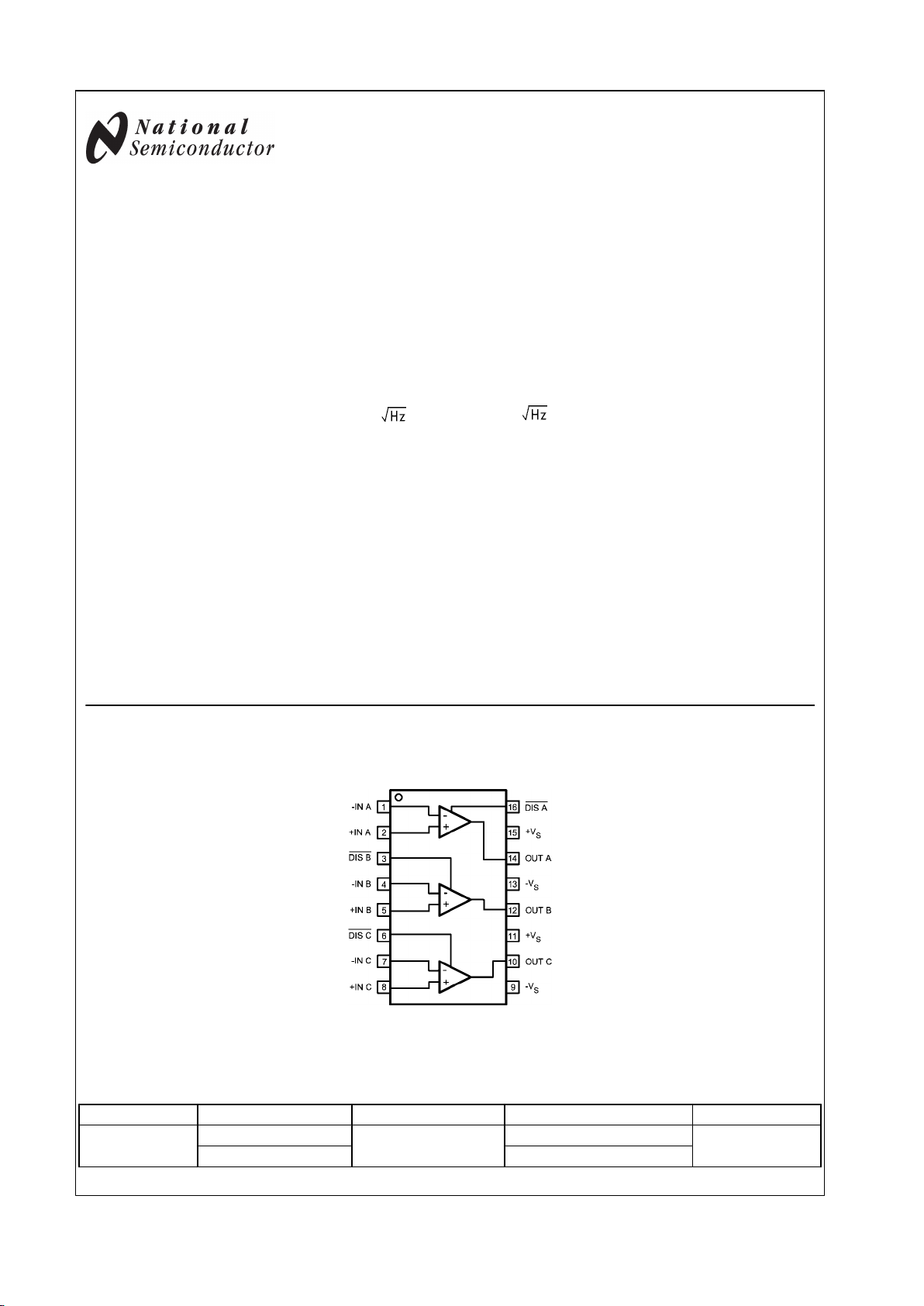
Connection Diagram
16-Pin SSOP
20199110
Top View
Ordering Information
Package Part Number Package Marking Transport Media NSC Drawing
16-pin SSOP
LMH6733MQ
LH6733MQ
95 Units/Rail
MQA16
LMH6733MQX 2.5k Units Tape and Reel
VIP10™ is a trademark of National Semiconductor Corporation.
© 2007 National Semiconductor Corporation 201991 www.national.com
LMH6733 Single Supply, 1.0 GHz, Triple Operational Amplifier
Page 2
Absolute Maximum Ratings (Note 1)
If Military/Aerospace specified devices are required,
please contact the National Semiconductor Sales Office/
Distributors for availability and specifications.
ESD Tolerance (Note 2)
Human Body Model 2000V
Machine Model 200V
Supply Voltage (V+ - V–)
13.2V
I
OUT
(Note 3)
Common Mode Input Voltage ±V
CC
Maximum Junction Temperature +150°C
Storage Temperature Range −65°C to +150°C
Soldering Information
Infrared or Convection (20 sec.) 235°C
Wave Soldering (10 sec.) 260°C
Storage Temperature Range −65°C to +150°C
Operating Ratings (Note 1)
Thermal Resistance
Package
(θJC)
(θJA)
16-Pin SSOP 36°C/W 120°C/W
Temperature Range (Note 4) −40°C +85°C
Supply Voltage (V+ - V–) 3V to 12V
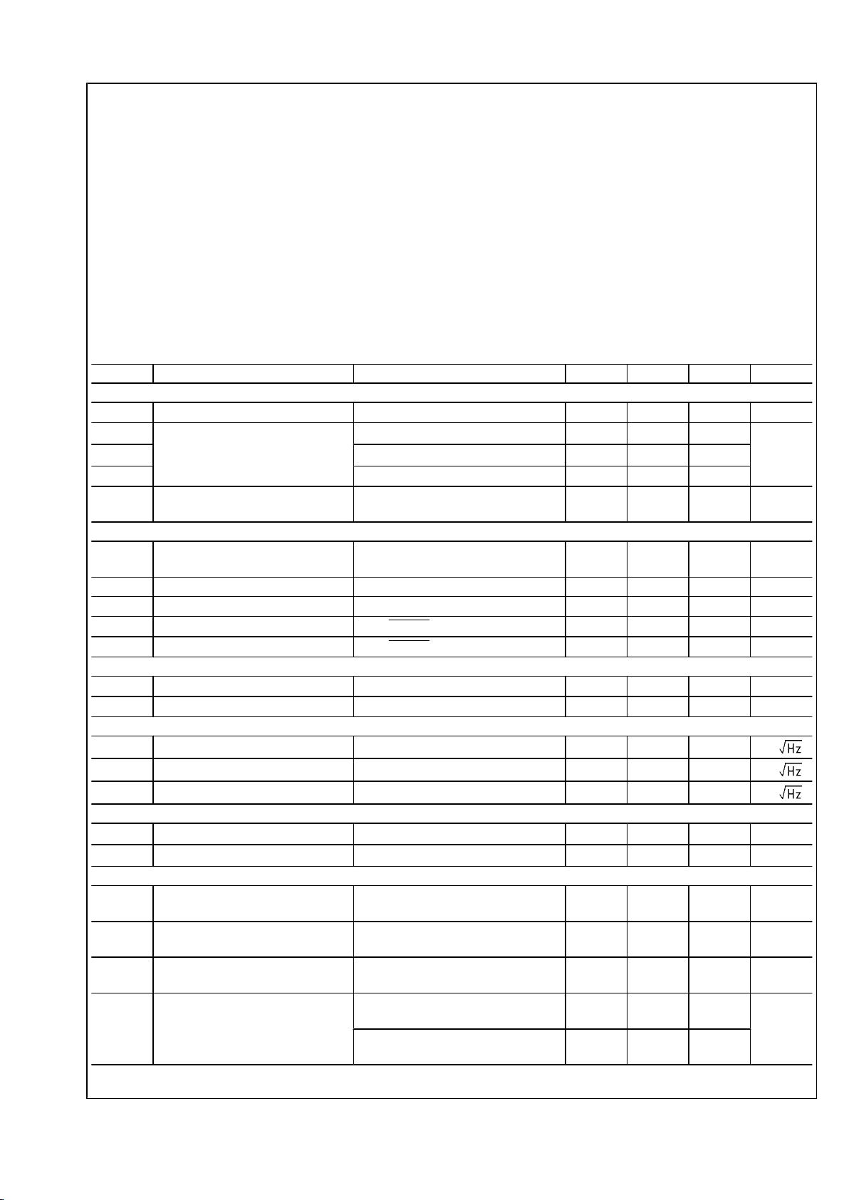
5V Electrical Characteristics (Note 5)
AV = +2, VCC = 5V, RL = 100Ω, RF = 340Ω; unless otherwise specified.
Symbol Parameter Conditions Min Typ Max Units
Frequency Domain Performance
UGBW −3 dB Bandwidth Unity Gain, V
OUT
= 200 mV
PP
870
MHz
SSBW −3 dB Bandwidth
V
OUT
= 200 mVPP, RL = 100Ω
650
MHz
SSBW
V
OUT
= 200 mVPP, RL = 150Ω
685
LSBW V
OUT
= 2 V
PP
480
0.1 dBBW0.1 dB Gain Flatness V
OUT
= 200 mV
PP
320 MHz
Time Domain Response
TRS Rise and Fall Time
(10% to 90%)
2V Step 0.8 ns
SR Slew Rate 2V Step 1900 V/µs
t
s
Settling Time to 0.1% 2V Step 10 ns
t
e
Enable Time From Disable = Rising Edge 10 ns
t
d
Disable Time From Disable = Falling Edge 15 ns
Distortion
HD2L 2nd Harmonic Distortion 2 VPP, 10 MHz −63 dBc
HD3L 3rd Harmonic Distortion 2 VPP, 10 MHz −73 dBc
Equivalent Input Noise
V
N
Non-Inverting Voltage >10 MHz 2.1
nV/
I
CN
Inverting Current >10 MHz 18.6
pA/
N
CN
Non-Inverting Current >10 MHz 26.9
pA/
Video Performance
DG Differential Gain
4.43 MHz, RL = 150Ω
0.03 %
DP Differential Phase
4.43 MHz, RL = 150Ω
0.025 deg
Static, DC Performance
VIO Input Offset Voltage (Note 7) 0.4 2.0
2.5
mV
IBN Input Bias Current (Note 7) Non-Inverting 2 16.7 28
32
µA
IBI Input Bias Current (Note 7) Inverting 1.0 17
19
μA
PSRR Power Supply Rejection Ratio
(Note 7)
+PSRR 59
59
61
dB
−PSRR 58
57
61
www.national.com 2
LMH6733
Page 3
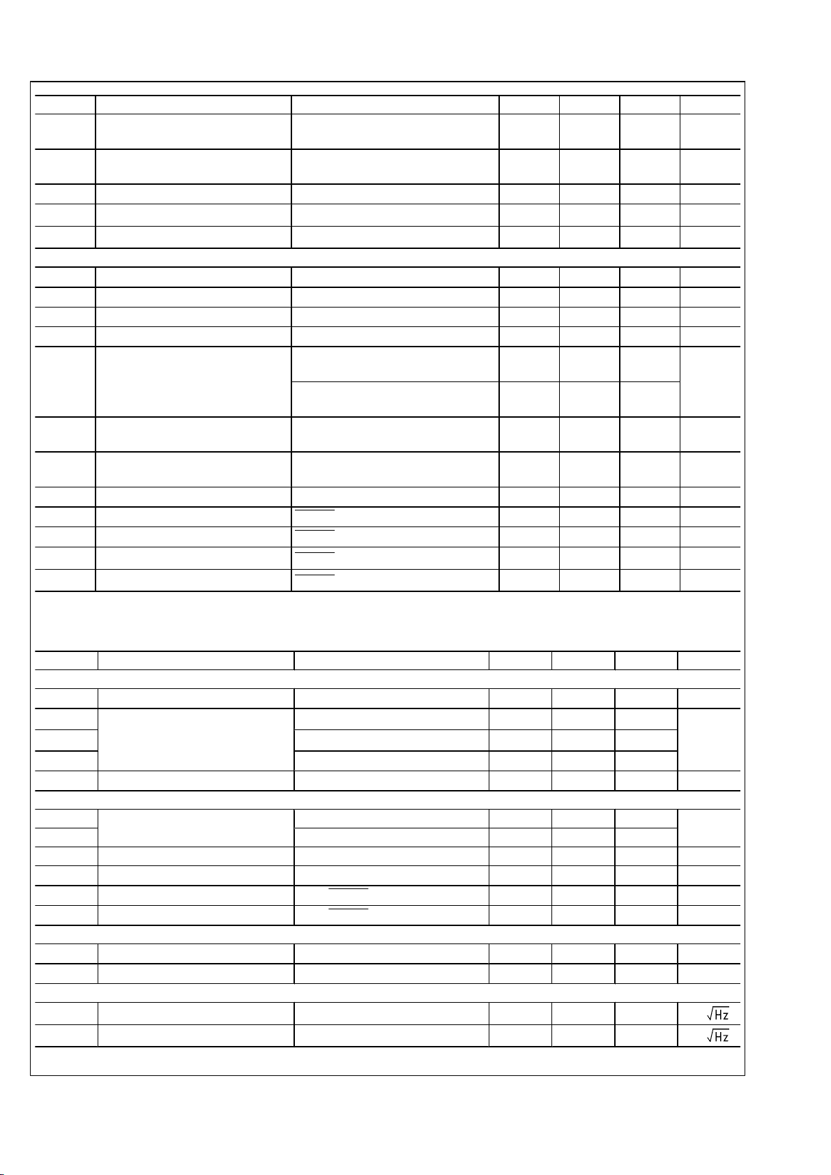
Symbol Parameter Conditions Min Typ Max Units
CMRR Common Mode Rejection Ratio
(Note 7)
52
51.5
54.5
dB
XTLK Crosstalk Input Referred, f = 10 MHz, Drive
Channels A,C Measure Channel B
−80 dB
I
CC
Supply Current (Note 7) All Three Amps Enabled, No Load 16.7 18 mA
Supply Current Disabled V
+
RL = ∞
1.54 1.8 mA
Supply Current Disabled V
−
RL = ∞
0.75 1.8 mA
Miscellaneous Performance
RIN+ Non-Inverting Input Resistance 200
kΩ
CIN+ Non-Inverting Input Capacitance 1 pF
RIN− Inverting Input Impedance Output Impedance of Input Buffer. 27
Ω
R
O
Output Impedance DC 0.05
Ω
V
O
Output Voltage Range (Note 7)
RL = 100Ω
1.25-3.75
1.3-3.7
1.12-3.88
V
RL = ∞
1.11-3.89
1.15-3.85
1.03-3.97
CMIR Common Mode Input Range
(Note 7)
CMRR > 40 dB 1.1-3.9
1.2-3.8
1.0–4.0
V
I
O
Linear Output Current
(Notes 3, 7)
VIN = 0V, V
OUT
< ±42 mV ±50 ±60 mA
I
SC
Short Circuit Current (Note 6) VIN = 2V Output Shorted to Ground 170 mA
I
IH
Disable Pin Bias Current High Disable Pin = V
+
−72
μA
I
IL
Disable Pin Bias Current Low Disable Pin = 0V −360
μA
V
DMAX
Voltage for Disable
Disable Pin ≤ V
DMAX
3.2 V
V
DMIM
Voltage for Enable
Disable Pin ≥ V
DMIN
3.6 V
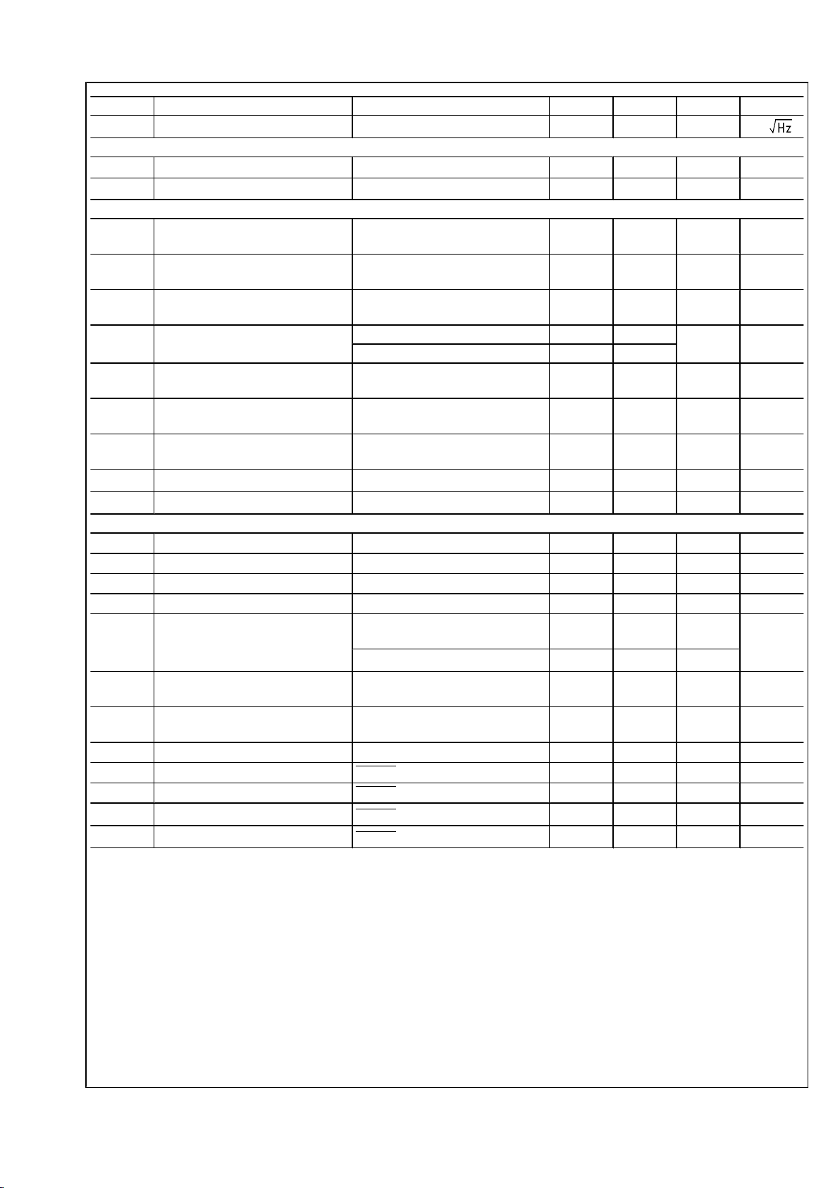
±5V Electrical Characteristics (Note 5)
AV = +2, VCC = ±5V, RL = 100Ω, RF = 383Ω; unless otherwise specified.
Symbol Parameter Conditions Min Typ Max Units
Frequency Domain Performance
UGBW −3 dB Bandwidth Unity Gain, V
OUT
= 200 mV
PP
1000 MHz
SSBW −3 dB Bandwidth
V
OUT
= 200 mVPP, RL = 100Ω
830
MHz
SSBW
V
OUT
= 200 mVPP, RL = 150Ω
950
LSBW V
OUT
= 2 V
PP
600
0.1 dB BW 0.1 dB Gain Flatness V
OUT
= 200 mV
PP
350
MHz
Time Domain Response
TRS Rise and Fall Time
(10% to 90%)
2V Step 0.7
ns
TRL 5V Step 0.8
SR Slew Rate 4V Step 3750 V/µs
t
s
Settling Time to 0.1% 2V Step 10 ns
t
e
Enable Time From Disable = Rising Edge 10 ns
t
d
Disable Time From Disable = Falling Edge 15 ns
Distortion
HD2L 2nd Harmonic Distortion 2 VPP, 10 MHz −72 dBc
HD3L 3rd Harmonic Distortion 2 VPP, 10 MHz −63 dBc
Equivalent Input Noise
V
N
Non-Inverting Voltage >10 MHz 2.1
nV/
I
CN
Inverting Current >10 MHz 18.6
pA/
3 www.national.com
LMH6733
Page 4
Symbol Parameter Conditions Min Typ Max Units
N
CN
Non-Inverting Current >10 MHz 26.9
pA/
Video Performance
DG Differential Gain
4.43 MHz, RL = 150Ω
0.03 %
DP Differential Phase
4.43 MHz, RL = 150Ω
0.03 Deg
Static, DC Performance
VIO Input Offset Voltage (Note 7) 0.6 2.2
2.5
mV
IBN Input Bias Current (Note 7) Non-Inverting −14
−19
3.5 19
24
µA
IBI Input Bias Current (Note 7) Inverting 5 23
26
μA
PSRR Power Supply Rejection Ratio
(Note 7)
+PSRR 59 61.5
dB
−PSRR 58 61
CMRR Common Mode Rejection Ratio
(Note 7)
53
52.5
55
dB
XTLK Crosstalk Input Referred, f = 10 MHz, Drive
Channels A,C Measure Channel B
−80 dB
I
CC
Supply Current (Note 7) All Three Amps Enabled, No Load 19.5 20.8
22.0
mA
Supply Current Disabled V
+
RL = ∞
1.54 1.8 mA
Supply Current Disabled V
−
RL = ∞
0.75 1.8 mA
Miscellaneous Performance
RIN+ Non-Inverting Input Resistance 200
kΩ
CIN+ Non-Inverting Input Capacitance 1 pF
RIN− Inverting Input Impedance Output Impedance of Input Buffer 30
Ω
R
O
Output Impedance DC 0.05
Ω
V
O
Output Voltage Range (Note 7)
RL = 100Ω
±3.55
±3.5
±3.7
V
RL = ∞
±3.85 ±4.0
CMIR Common Mode Input Range
(Note 7)
CMRR > 43 dB ±3.9
±3.8
±4.0 V
I
O
Linear Output Current
(Notes 3, 7)
VIN = 0V, V
OUT
< ±42 mV 70 ±80 mA
I
SC
Short Circuit Current (Note 6) VIN = 2V Output Shorted to Ground 237 mA
I
IH
Disable Pin Bias Current High Disable Pin = V
+
−72
μA
I
IL
Disable Pin Bias Current Low Disable Pin = 0V −360
μA
V
DMAX
Voltage for Disable
Disable Pin ≤ V
DMAX
3.2 V
V
DMIM
Voltage for Enable
Disable Pin ≥ V
DMIN
3.6 V
Note 1: Absolute Maximum Ratings indicate limits beyond which damage to the device may occur. Operating Ratings indicate conditions for which the device is
intended to be functional, but specific performance is not guaranteed. For guaranteed specifications, see the Electrical Characteristics tables.
Note 2: Human Body Model, applicable std. MIL-STD-883, Method 3015.7. Machine Model, applicable std. JESD22-A115-A (ESD MM std. of JEDEC)
Field-Induced Charge-Device Model, applicable std. JESD22-C101-C (ESD FICDM std. of JEDEC).
Note 3: The maximum output current (I
OUT
) is determined by device power dissipation limitations. See the Power Dissipation section of the Applications Information
for more details.
Note 4: The maximum power dissipation is a function of T
J(MAX)
, θJA. The maximum allowable power dissipation at any ambient temperature is
PD = (T
J(MAX)
– TA)/ θJA. All numbers apply for packages soldered directly onto a PC Board.
Note 5: Electrical Table values apply only for factory testing conditions at the temperature indicated. Factory testing conditions result in very limited self-heating
of the device such that TJ = TA. No guarantee of parametric performance is indicated in the electrical tables under conditions of internal self-heating where
TJ > TA.
Note 6: Short circuit current should be limited in duration to no more than 10 seconds. See the Power Dissipation section of the Application Section for more
details.
Note 7: Parameter 100% production tested at 25° C.
www.national.com 4
LMH6733
Page 5
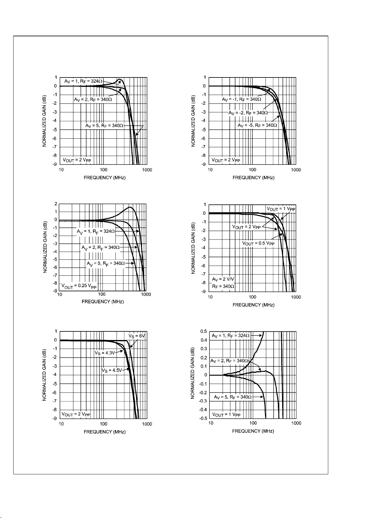
Typical Performance Characteristics A
V
= +2, VCC = 5V, RL = 100Ω, RF = 340Ω; unless otherwise
specified).
Large Signal Frequency Response
20199111
Large Signal Frequency Response
20199112
Small Signal Frequency Response
20199113
Frequency Response vs. V
OUT
20199114
Frequency Response vs. Supply Voltage
20199115
Gain Flatness
20199116
5 www.national.com
LMH6733
Page 6

Pulse Response
20199128
Crosstalk vs. Frequency
20199121
Distortion vs. Frequency
20199133
Distortion vs. Output Voltage
20199134
Small Signal Frequency Response vs. R
L
20199135
Frequency Response vs. Capacitive Load
20199136
www.national.com 6
LMH6733
Page 7

Series Output Resistance vs. Capacitive Load
20199137
PSRR vs. Frequency
20199138
CMRR vs. Frequency
20199139
Closed Loop Output Impedance |Z|
20199140
Disabled Channel Isolation vs. Frequency
20199141
Disable Timing
20199142
7 www.national.com
LMH6733
Page 8

DC Errors vs. Temperature
20199143
Open Loop Transimpedance
20199145
Input Noise vs. Frequency
20199146
www.national.com 8
LMH6733
Page 9

Typical Performance Characteristics A
V
= +2, VCC = ±5V, RL = 100Ω, RF = 383Ω; unless otherwise
specified).
Large Signal Frequency Response
20199122
Large Signal Frequency Response
20199123
Small Signal Frequency Response
20199124
Frequency Response vs. V
OUT
20199125
Frequency Response vs. Supply Voltage
20199126
Gain Flatness
20199127
9 www.national.com
LMH6733
Page 10

Pulse Response
20199128
Crosstalk vs. Frequency
20199129
Distortion vs. Output Voltage
20199130
Distortion vs. Frequency
20199131
DC Errors vs. Temperature
20199144
www.national.com 10
LMH6733
Page 11

Application Information
20199105
FIGURE 1. Recommended Non-Inverting Gain Circuit
20199106
FIGURE 2. Recommended Inverting Gain Circuit
GENERAL INFORMATION
The LMH6733 is a high speed current feedback amplifier, optimized for very high speed and low distortion. The LMH6733
has no internal ground reference so single or split supply configurations are both equally useful.
FEEDBACK RESISTOR SELECTION
One of the key benefits of a current feedback operational amplifier is the ability to maintain optimum frequency response
independent of gain by using the appropriate values for the
feedback resistor (RF). The Electrical Characteristics and
Typical Performance plots specify an RF of 340Ω, a gain of
+2 V/V and ±2.5V power supplies (unless otherwise specified). Generally, lowering RF from its recommended value will
peak the frequency response and extend the bandwidth while
increasing the value of RF will cause the frequency response
to roll off faster. Reducing the value of RF too far below its
recommended value will cause overshoot, ringing and, eventually, oscillation.
20199103
FIGURE 3. Recommended RF vs. Gain
See Figure 3 for selecting a feedback resistor value for gains
of ±1 to ±10. Since each application is slightly different it is
worth some experimentation to find the optimal RF for a given
circuit. In general a value of RF that produces about 0.1 dB of
peaking is the best compromise between stability and maximal bandwidth. Note that it is not possible to use a current
feedback amplifier with the output shorted directly to the inverting input. The buffer configuration of the LMH6733 requires a 324Ω feedback resistor for stable operation.
The LMH6733 has been optimized for high speed operation.
As shown in Figure 3 the suggested value for RF decreases
for higher gains. Due to the impedance of the input buffer
there is a practical limit for how small RF can go, based on the
lowest practical value of RG. This limitation applies to both
inverting and non-inverting configurations. For the LMH6733
the input resistance of the inverting input is approximately
30Ω and 20Ω is a practical (but not hard and fast) lower limit
for RG. The LMH6733 begins to operate in a gain bandwidth
limited fashion in the region where RG is nearly equal to the
input buffer impedance. Note that the amplifier will operate
with RG values well below 20Ω, however results may be substantially different than predicted from ideal models. In particular the voltage potential between the inverting and noninverting inputs cannot be expected to remain small.
Inverting gain applications that require impedance matched
inputs may limit gain flexibility somewhat (especially if maximum bandwidth is required). The impedance seen by the
source is RG || RT (RT is optional). The value of RG is RF /gain.
Thus for an inverting gain of −5 V/V and an optimal value for
RF the input impedance is equal to 55Ω. Using a termination
resistor this can be brought down to match a 25Ω source;
however, a 150Ω source cannot be matched. To match a
150Ω source would require using a 1050Ω feedback resistor
and would result in reduced bandwidth.
For more information see Application Note OA-13 which describes the relationship between RF and closed-loop frequency response for current feedback operational amplifiers. The
value for the inverting input impedance for the LMH6733 is
approximately 30Ω. The LMH6733 is designed for optimum
performance at gains of +1 to +10 V/V and −1 to −9 V/V.
Higher gain configurations are still useful; however, the bandwidth will fall as gain is increased, much like a typical voltage
feedback amplifier.
11 www.national.com
LMH6733
Page 12

ACTIVE FILTER
The choice of reactive components requires much attention
when using any current feedback operational amplifier as an
active filter. Reducing the feedback impedance, especially at
higher frequencies, will almost certainly cause stability problems. Likewise capacitance on the inverting input should be
avoided. See Application Notes OA-7 and OA-26 for more information on Active Filter applications for Current Feedback
Op Amps.
When using the LMH6733 as a low pass filter the value of
RF can be substantially reduced from the value recommended
in the RF vs. Gain charts. The benefit of reducing RF is increased gain at higher frequencies, which improves attenuation in the stop band. Stability problems are avoided because
in the stop band additional device bandwidth is used to cancel
the input signal rather than amplify it. The benefit of this
change depends on the particulars of the circuit design. With
a high pass filter configuration reducing RF will likely result in
device instability and is not recommended.
20199107
FIGURE 4. Typical Video Application
20199108
FIGURE 5. Decoupling Capacitive Loads
DRIVING CAPACITIVE LOADS
Capacitive output loading applications will benefit from the
use of a series output resistor R
OUT
. Figure 5 shows the use
of a series output resistor, R
OUT
, to stabilize the amplifier output under capacitive loading. Capacitive loads of 5 to 120 pF
are the most critical, causing ringing, frequency response
peaking and possible oscillation. The chart “Frequency Response vs. Capacitive Load” give a recommended value for
selecting a series output resistor for mitigating capacitive
loads. The values suggested in the charts are selected for .5
dB or less of peaking in the frequency response. This gives a
good compromise between settling time and bandwidth. For
applications where maximum frequency response is needed
and some peaking is tolerable, the value of R
OUT
can be re-
duced slightly from the recommended values.
www.national.com 12
LMH6733
Page 13

20199132
FIGURE 6. AC Coupled Single Supply Video Amplifier
AC-COUPLED VIDEO
The LMH6733 can be used as an AC-coupled single supply
video amplifier for driving 75Ω coax with a gain of 2. The input
signal is nominally 0.7V or 1.0V for component YPRPB and
RGB, depending on the presence of a sync. R1, R2, and R
3
simply set the input to the center of the input linear range while
CIN AC couples the video onto the op amp’s input.
As can be seen in Figure 6, amplifier U1 is used in a positive
gain configuration set for a closed loop gain of 2. The feedback resistor RF is 340Ω. The gain resistor is created from the
parallel combination of RG and R4, giving a Thevenin equivalent of 340Ω connected to 2.5V.
The 75Ω back termination resistor RO divides the signal such
that V
OUT
equals a buffered version of VIN. The back termination will eliminate any reflection of the signal that comes
from the load. The input termination resistor, RT, is optional –
it is used only if matching of the incoming line is necessary.
In some applications, it is recommended that a small valued
ceramic capacitor be used in parallel with CO which is itself
electrolytic because of its rather large value. The ceramic cap
will tend to shunt the inductive behavior of this electrolytic cap,
CO, at higher frequencies for an improved overall, lowimpedance output.
INVERTING INPUT PARASITIC CAPACITANCE
Parasitic capacitance is any capacitance in a circuit that was
not intentionally added. It comes about from electrical interaction between conductors. Parasitic capacitance can be
reduced but never entirely eliminated. Most parasitic capacitances that cause problems are related to board layout or lack
of termination on transmission lines. Please see the section
on Layout Considerations for hints on reducing problems due
to parasitic capacitances on board traces. Transmission lines
should be terminated in their characteristic impedance at both
ends.
High speed amplifiers are sensitive to capacitance between
the inverting input and ground or power supplies. This shows
up as gain peaking at high frequency. The capacitor raises
device gain at high frequencies by making RG appear smaller.
Capacitive output loading will exaggerate this effect. In gen-
eral, avoid introducing unnecessary parasitic capacitance at
both the inverting input and the output.
One possible remedy for this effect is to slightly increase the
value of the feedback (and gain set) resistor. This will tend to
offset the high frequency gain peaking while leaving other
parameters relatively unchanged. If the device has a capacitive load as well as inverting input capacitance using a series
output resistor as described in the section on “Driving Capacitive Loads” will help.
LAYOUT CONSIDERATIONS
Whenever questions about layout arise, use the evaluation
board as a guide. The LMH730275 is the evaluation board
supplied with samples of the LMH6733.
To reduce parasitic capacitances ground and power planes
should be removed near the input and output pins. Components in the feedback loop should be placed as close to the
device as possible. For long signal paths controlled
impedance lines should be used, along with impedance
matching elements at both ends.
Bypass capacitors should be placed as close to the device as
possible. Bypass capacitors from each rail to ground are applied in pairs. The larger electrolytic bypass capacitors can be
located farther from the device, the smaller ceramic capacitors should be placed as close to the device as possible. The
LMH6733 has multiple power and ground pins for enhanced
supply bypassing. Every pin should ideally have a separate
bypass capacitor. Sharing bypass capacitors may slightly degrade second order harmonic performance, especially if the
supply traces are thin and /or long. In Figure 1 and Figure 2
CSS is optional, but is recommended for best second harmonic distortion. Another option to using CSS is to use pairs of .01
μF and .1 μF ceramic capacitors for each supply bypass.
VIDEO PERFORMANCE
The LMH6733 has been designed to provide excellent performance with production quality video signals in a wide variety of formats such as HDTV and High Resolution VGA.
NTSC and PAL performance is nearly flawless. Best performance will be obtained with back terminated loads. The back
13 www.national.com
LMH6733
Page 14

termination reduces reflections from the transmission line and
effectively masks transmission line and other parasitic capacitances from the amplifier output stage. Figure 4 shows a
typical configuration for driving a 75Ω cable. The amplifier is
configured for a gain of two to make up for the 6 dB of loss in
R
OUT
.
20199102
FIGURE 7. Maximum Power Dissipation
POWER DISSIPATION
The LMH6733 is optimized for maximum speed and performance in the small form factor of the standard SSOP-16
package. To achieve its high level of performance, the
LMH6733 consumes an appreciable amount of quiescent
current which cannot be neglected when considering the total
package power dissipation limit. The quiescent current contributes to about 40° C rise in junction temperature when no
additional heat sink is used (VS = ±5V, all 3 channels on).
Therefore, it is easy to see that proper precautions need to
be taken in order to make sure the junction temperature’s absolute maximum rating of 150°C is not violated.
To ensure maximum output drive and highest performance,
thermal shutdown is not provided. Therefore, it is of utmost
importance to make sure that the T
JMAX
is never exceeded
due to the overall power dissipation (all 3 channels).
With the LMH6733 used in a back-terminated 75Ω RGB ana-
log video system (with 2 VPP output voltage), the total power
dissipation is around 305 mW of which 220 mW is due to the
quiescent device dissipation (output black level at 0V). With
no additional heat sink used, that puts the junction temperature to about 120° C when operated at 85°C ambient.
To reduce the junction temperature many options are available. Forced air cooling is the easiest option. An external addon heat-sink can be added to the SSOP-16 package, or
alternatively, additional board metal (copper) area can be utilized as heat-sink.
An effective way to reduce the junction temperature for the
SSOP-16 package (and other plastic packages) is to use the
copper board area to conduct heat. With no enhancement the
major heat flow path in this package is from the die through
the metal lead frame (inside the package) and onto the surrounding copper through the interconnecting leads. Since
high frequency performance requires limited metal near the
device pins the best way to use board copper to remove heat
is through the bottom of the package. A gap filler with high
thermal conductivity can be used to conduct heat from the
bottom of the package to copper on the circuit board. Vias to
a ground or power plane on the back side of the circuit board
will provide additional heat dissipation. A combination of front
side copper and vias to the back side can be combined as
well.
Follow these steps to determine the maximum power dissipation for the LMH6733:
1.
Calculate the quiescent (no-load) power: P
AMP
= ICC X
(VS), where VS = V+-V
−
2.
Calculate the RMS power dissipated in the output stage:
PD (rms) = rms ((VS - V
OUT
) X I
OUT
) where V
OUT
and
I
OUT
are the voltage and the current across the external
load and VS is the total supply voltage
3.
Calculate the total RMS power: PT = P
AMP+PD
The maximum power that the LMH6733, package can dissipate at a given temperature can be derived with the following
equation (See Figure 7):
P
MAX
= (150°C/W– T
AMB
)/ θJA, where T
AMB
= ambient tem-
perature (°C) and θJA = thermal resistance, from junction to
ambient, for a given package (°C/W). For the SSOP package
θJA is 120°C/W.
ESD PROTECTION
The LMH6733 is protected against electrostatic discharge
(ESD) on all pins. The LMH6733 will survive 2000V Human
Body Model and 200V Machine Model events.
Under closed loop operation the ESD diodes have no affect
on circuit performance. There are occasions, however, when
the ESD diodes will be evident. If the LMH6733 is driven by
a large signal while the device is powered down the ESD
diodes will conduct.
The current that flows through the ESD diodes will either exit
the chip through the supply pins or will flow through the device, hence it is possible to power up a chip with a large signal
applied to the input pins. Shorting the power pins to each other
will prevent the chip from being powered up through the input.
EVALUATION BOARDS
National Semiconductor provides the following evaluation
boards as a guide for high frequency layout and as an aid in
device testing and characterization. Many of the datasheet
plots were measured with these boards.
Device Package Evaluation Board
Part Number
LMH6733MQ SSOP LMH730275
A bare evaluation board can be ordered when a sample request is placed with National Semiconductor.
www.national.com 14
LMH6733
Page 15

Physical Dimensions inches (millimeters) unless otherwise noted
16-Pin SSOP
NS Package Number MQA16
15 www.national.com
LMH6733
Page 16

Notes
LMH6733 Single Supply, 1.0 GHz, Triple Operational Amplifier
THE CONTENTS OF THIS DOCUMENT ARE PROVIDED IN CONNECTION WITH NATIONAL SEMICONDUCTOR CORPORATION
(“NATIONAL”) PRODUCTS. NATIONAL MAKES NO REPRESENTATIONS OR WARRANTIES WITH RESPECT TO THE ACCURACY
OR COMPLETENESS OF THE CONTENTS OF THIS PUBLICATION AND RESERVES THE RIGHT TO MAKE CHANGES TO
SPECIFICATIONS AND PRODUCT DESCRIPTIONS AT ANY TIME WITHOUT NOTICE. NO LICENSE, WHETHER EXPRESS,
IMPLIED, ARISING BY ESTOPPEL OR OTHERWISE, TO ANY INTELLECTUAL PROPERTY RIGHTS IS GRANTED BY THIS
DOCUMENT.
TESTING AND OTHER QUALITY CONTROLS ARE USED TO THE EXTENT NATIONAL DEEMS NECESSARY TO SUPPORT
NATIONAL’S PRODUCT WARRANTY. EXCEPT WHERE MANDATED BY GOVERNMENT REQUIREMENTS, TESTING OF ALL
PARAMETERS OF EACH PRODUCT IS NOT NECESSARILY PERFORMED. NATIONAL ASSUMES NO LIABILITY FOR
APPLICATIONS ASSISTANCE OR BUYER PRODUCT DESIGN. BUYERS ARE RESPONSIBLE FOR THEIR PRODUCTS AND
APPLICATIONS USING NATIONAL COMPONENTS. PRIOR TO USING OR DISTRIBUTING ANY PRODUCTS THAT INCLUDE
NATIONAL COMPONENTS, BUYERS SHOULD PROVIDE ADEQUATE DESIGN, TESTING AND OPERATING SAFEGUARDS.
EXCEPT AS PROVIDED IN NATIONAL’S TERMS AND CONDITIONS OF SALE FOR SUCH PRODUCTS, NATIONAL ASSUMES NO
LIABILITY WHATSOEVER, AND NATIONAL DISCLAIMS ANY EXPRESS OR IMPLIED WARRANTY RELATING TO THE SALE
AND/OR USE OF NATIONAL PRODUCTS INCLUDING LIABILITY OR WARRANTIES RELATING TO FITNESS FOR A PARTICULAR
PURPOSE, MERCHANTABILITY, OR INFRINGEMENT OF ANY PATENT, COPYRIGHT OR OTHER INTELLECTUAL PROPERTY
RIGHT.
LIFE SUPPORT POLICY
NATIONAL’S PRODUCTS ARE NOT AUTHORIZED FOR USE AS CRITICAL COMPONENTS IN LIFE SUPPORT DEVICES OR
SYSTEMS WITHOUT THE EXPRESS PRIOR WRITTEN APPROVAL OF THE CHIEF EXECUTIVE OFFICER AND GENERAL
COUNSEL OF NATIONAL SEMICONDUCTOR CORPORATION. As used herein:
Life support devices or systems are devices which (a) are intended for surgical implant into the body, or (b) support or sustain life and
whose failure to perform when properly used in accordance with instructions for use provided in the labeling can be reasonably expected
to result in a significant injury to the user. A critical component is any component in a life support device or system whose failure to perform
can be reasonably expected to cause the failure of the life support device or system or to affect its safety or effectiveness.
National Semiconductor and the National Semiconductor logo are registered trademarks of National Semiconductor Corporation. All other
brand or product names may be trademarks or registered trademarks of their respective holders.
Copyright© 2007 National Semiconductor Corporation
For the most current product information visit us at www.national.com
National Semiconductor
Americas Customer
Support Center
Email:
new.feedback@nsc.com
Tel: 1-800-272-9959
National Semiconductor Europe
Customer Support Center
Fax: +49 (0) 180-530-85-86
Email: europe.support@nsc.com
Deutsch Tel: +49 (0) 69 9508 6208
English Tel: +49 (0) 870 24 0 2171
Français Tel: +33 (0) 1 41 91 8790
National Semiconductor Asia
Pacific Customer Support Center
Email: ap.support@nsc.com
National Semiconductor Japan
Customer Support Center
Fax: 81-3-5639-7507
Email: jpn.feedback@nsc.com
Tel: 81-3-5639-7560
www.national.com
 Loading...