

Page 1
LMH6718
Dual, High Output, Programmable Gain Buffer
General Description
The LMH6718 is a dual, low cost high speed (130MHz)
buffer which features user programmable gains of +2, +1,
and -1V/V. The LMH6718 also has a new output stage that
delivers high output drive current (200mA), but consumes
minimal quiescent supply current (2.6mA/Amp) from a
±
5V
supply. Its current feedback architecture, fabricated in an
advanced complementary bipolar process, maintains consistent performance over a wide range of signal levels, and has
a linear phase response up to one half of the -3dB frequency.
The LMH6718 offers 0.1dB gain flatness to 30MHz and
differential gain and phase errors of .04% and .03˚. These
features are ideal for professional and consumer video applications.
The LMH6718 offers superior dynamic performance with a
130MHz small-signal bandwidth, 600V/µs slew rate and
4.2ns rise/fall times (2V
STEP
). The combination of low quiescent current, high output current drive, and high speed performance makes the LMH6718 well suited for many battery
powered personal communication/computing systems. The
ability to drive low impedance, high capacitive loads, makes
the LMH6718 ideal for single ended cable applications. It
also drives low impedance loads with minimum distortion.
The LMH6718 will drive a 100Ω load with only −84/−84dBc
second/third harmonic distortion (A
V
= +2, V
OUT
=2VPP,f=
1MHz). It is also optimized for driving high currents into
single-ended transformers and coils. When driving the input
of high resolution A/D converters, the LMH6718 provides
excellent -88/-98dBc second/third harmonic distortion (A
V
=
+2, V
OUT
=2VPP, f = 1MHz, RL=1kΩ) and fast settling time.
The LMH6718 is fabricated using National’s VIP10
™
com-
plimentary bipolar process.
Features
n 200mA output current
n .04%, .03˚ differential gain, phase
n 5.2mA supply current for 2 amplifiers
n 130MHz bandwidth (A
V
= +2)
n −88/−98dBc HD2/HD3 (1MHz)
n 16ns settling to 0.05%
n 600V/µs slew rate
n Nominal supply range
±
2.5V to±6V
n Improved replacement for CLC5632
Applications
n Video line driver
n Coaxial cable driver
n Twisted pair driver
n Transformer/coil driver
n High capacitive load driver
n Portable/battery powered applications
n A/D driver
n I/Q Channel Amplifier
Connection Diagram
8-Pin SOIC
20040116
Top View
Maximum Output Voltage vs. Load
Resistance
20040164
January 2003
LMH6718 Dual, High Output, Programmable Gain Buffer
© 2003 National Semiconductor Corporation DS200401 www.national.com
Page 2
Absolute Maximum Ratings (Note 1)
If Military/Aerospace specified devices are required,
please contact the National Semiconductor Sales Office/
Distributors for availability and specifications.
ESD Tolerance (Note 5)
Human Body Model 2kV
Machine Model 200V
Supply Voltage 13.5
Output Current (Note 3)
Common-Mode Input Voltage V
+-V−
Maximum Junction Temperature +150˚C
Storage Temperature Range −65˚C to +150˚C
Lead Temperature (Soldering 10 sec) +300˚C
Operating Ratings
Thermal Resistance
Package (θ
JC
)(θJA)
SOIC 50˚C/W 145˚C/W
Nominal Operating Voltage
±
2.5V to±6V
Operating Temperature Range −40˚C to +85˚C
+5V Electrical Characteristics (Note 2)
AV= +2, RL= 100Ω,VS= +5V (Note 4), Unless Specified. Boldface limits apply at the temperature extremes.
Symbol Parameter Conditions Min Typ Max Units
Frequency Domain Response
SSBW -3dB Bandwidth V
O
=0.5V
PP
70 110
MHz
V
O
=2.0V
PP
90
SSBW −0.1dB Bandwidth V
O
=0.5V
PP
23 MHz
GFP Gain Peaking
<
200MHz, VO=0.5V
PP
0dB
GFR Gain Rolloff
<
30MHz, VO=0.5V
PP
0.2 dB
LPD Linear Phase Deviation
<
30MHz, VO= 0.5V
PP
0.12 deg
Time Domain Response
Tr Rise and Fall Time 2V Step 4.8 ns
Ts Settling Time to 0.05% 1V Step 20 ns
OS Overshoot 2V Step 5 %
SR Slew Rate 2V Step 250 400 V/µs
Distortion And Noise Response
HD2 2nd Harmonic Distortion 2V
PP
, 1MHz −85
dBc2V
PP
, 1MHz; RL=1kΩ −88
2V
PP
, 5MHz −73
HD3 3rd Harmonic Distortion 2V
PP
,1MHz −89
dBc2V
PP
, 1MHz, RL=1kΩ −91
2V
PP
, 5MHz −71
XTLKA Crosstalk (Input Referred) 10MHz, 1V
PP
−85 dB
Static, DC Performance
V
IO
Input Offset Voltage
±
.6
±
10
±
20
mV
DV
IO
Average Drift 10 µV/˚C
I
BN
Input Bias Current
(Non-Inverting)
±
.6
±
15
±
20
µA
DI
BN
Average Drift 20 nA/˚C
GACC Gain Accuracy
±
0.3
±
1.5
±
2.0
%
Internal Resistors (R
F,RG
) 750 950 1150 Ω
PSRR Power supply Rejection Ratio DC 50 60 dB
CMRR Common Mode Rejection Ratio DC 50
47
56
dB
I
CC
Supply Current per channel RL=
∞
2.0
1.9
2.4 3.0
3.1
mA
Miscellaneous Performance
R
IN
Input Resistance (Non-Inverting) 0.38 MΩ
LMH6718
www.national.com 2
Page 3
+5V Electrical Characteristics (Note 2) (Continued)
AV= +2, RL= 100Ω,VS= +5V (Note 4), Unless Specified. Boldface limits apply at the temperature extremes.
Symbol Parameter Conditions Min Typ Max Units
C
IN
Input Capacitance
(Non-Inverting)
2.2 pF
V
CMH
Input Voltage Range, High 4.2 V
V
CML
Input Voltage Range, Low 0.8 V
V
ROH
Output Voltage Range, High RL= 100Ω 3.6
3.5
4.0
V
V
ROL
Output Voltage Range, Low RL= 100Ω 1.4
1.3
1.0
V
V
ROH
Output Voltage Range, High RL=
∞
4.1 V
V
ROL
Output Voltage Range, Low RL=
∞
0.9 V
I
O
Output Current (Note 3) 170 mA
R
O
Output Resistance, Closed Loop DC .28 Ω
±
5V Electrical Characteristics (Note 2)
AV= +2, RL= 100Ω,VCC=±5V; Unless Specified. Boldface limits apply at the temperature extremes.
Symbol Parameter Conditions Min Typ Max Units
Frequency Domain Response
SSBW -3dB Bandwidth V
O
=1.0V
PP
100 130
MHz
V
O
=4.0V
PP
70
SSBW −0.1dB Bandwidth V
O
= 1.0V
PP
30 MHz
GFP Gain Peaking
<
200MHz, VO= 1.0V
PP
0dB
GFR Gain Rolloff
<
300MHz, VO= 1.0V
PP
0.1 dB
LPD Linear Phase Deviation
<
30MHz, VO= 1.0V
PP
0.1 deg
DG Differential Gain NTSC, R
L
= 150Ω .04 %
DP Differential Phase NTSC, R
L
= 150Ω .03 deg
Time Domain Response
Tr Rise and Fall Time 2V Step 4.2 ns
Ts Settling Time to 0.05% 2V Step 17 ns
OS Overshoot 2V Step 14 %
SR Slew Rate 2V Step 400 600 V/µs
Distortion And Noise Response
HD2 2nd Harmonic Distortion 2V
PP
,1MHz −84
dBc2V
PP
, 1MHz; RL=1kΩ −88
2V
PP
, 5MHz −73
HD3 3rd Harmonic Distortion 2V
PP
,1MHz −84
dBc2V
PP
, 1MHz; RL=1kΩ −98
2V
PP
, 5MHz −76
Equivalent Input Noise
V
N
Voltage (eni)
>
1MHz 8 nV/
I
NN
Non-Inverting Current (ibn)
>
1MHz 9 pA/
XTLKA Crosstalk (Input Referred) 10MHz, 1V
PP
−85 dB
Static, DC Performance
V
IO
Input Offset Voltage .2
±
9.5
±
15
mV
DV
IO
Average Drift 5 µV/˚C
I
BN
Input Bias Current
(Non-Inverting)
1.3
±
15
±
20
µA
DI
BN
Average Drift 12 nA/˚C
LMH6718
www.national.com3
Page 4
±
5V Electrical Characteristics (Note 2) (Continued)
AV= +2, RL= 100Ω,VCC=±5V; Unless Specified. Boldface limits apply at the temperature extremes.
Symbol Parameter Conditions Min Typ Max Units
GACC Gain Accuracy
±
0.3
±
1.5
±
2.0
%
Internal Resistor (R
F,RG
) 750 950 1150 Ω
PSRR Power Supply Rejection Ratio DC 50 62 dB
CMRR Common Mode Rejection Ratio DC 52
49
57
dB
I
CC
Supply Current per channel RL=
∞
2.2
2.1
2.6 3.3
3.4
mA
Miscellaneous Performance
R
IN
Input Resistance (Non-Inverting) 0.50 MΩ
C
IN
Input Capacitance
(Non-Inverting)
1.9 pF
CMVR Common-Mode Voltage Range
±
4.2 V
V
RO
Output Voltage Range RL= 100Ω 3.6
3.5
±
3.8
V
V
RO
Output Voltage Range RL=
∞
±
4.0 V
I
O
Output Current (Note 3) 200 mA
R
O
Output Resistance, Closed Loop DC .28 Ω
Note 1: Absolute Maximum Ratings indicate limits beyond which damage to the device may occur. Operating Ratings indicate conditions for which the device is
intended to be functional, but specific performance is not guaranteed. For guaranteed specifications, see the Electrical Characteristics tables.
Note 2: Electrical Table values apply only for factory testing conditions at the temperature indicated. Factory testing conditions result in very limited self-heating of
the device such that T
J=TA
. No guarantee of parametric performance is indicated in the electrical tables under conditions of internal self heating where T
J
>
TA.
See Applications Section for information on temperature de-rating of this device." Min/Max ratings are based on product characterization and simulation. Individual
parameters are tested as noted.
Note 3: The maximum current is determined by device power dissipation limitations. See the Power Dissipation section of the Application Division for more details.
Note 4: V
S=VCC−VEE
Note 5: Human body model, 1.5kΩ in series with 100pF. Machine model, 0Ω In series with 200pF.
Ordering Information
Package Part Number Package Marking Transport Media NSC Drawing
8-pin SOIC LMH6718MA LMH6718MA Rails M08A
LMH6718IMAX 2.5k Units Tape and Reel
LMH6718
www.national.com 4
Page 5
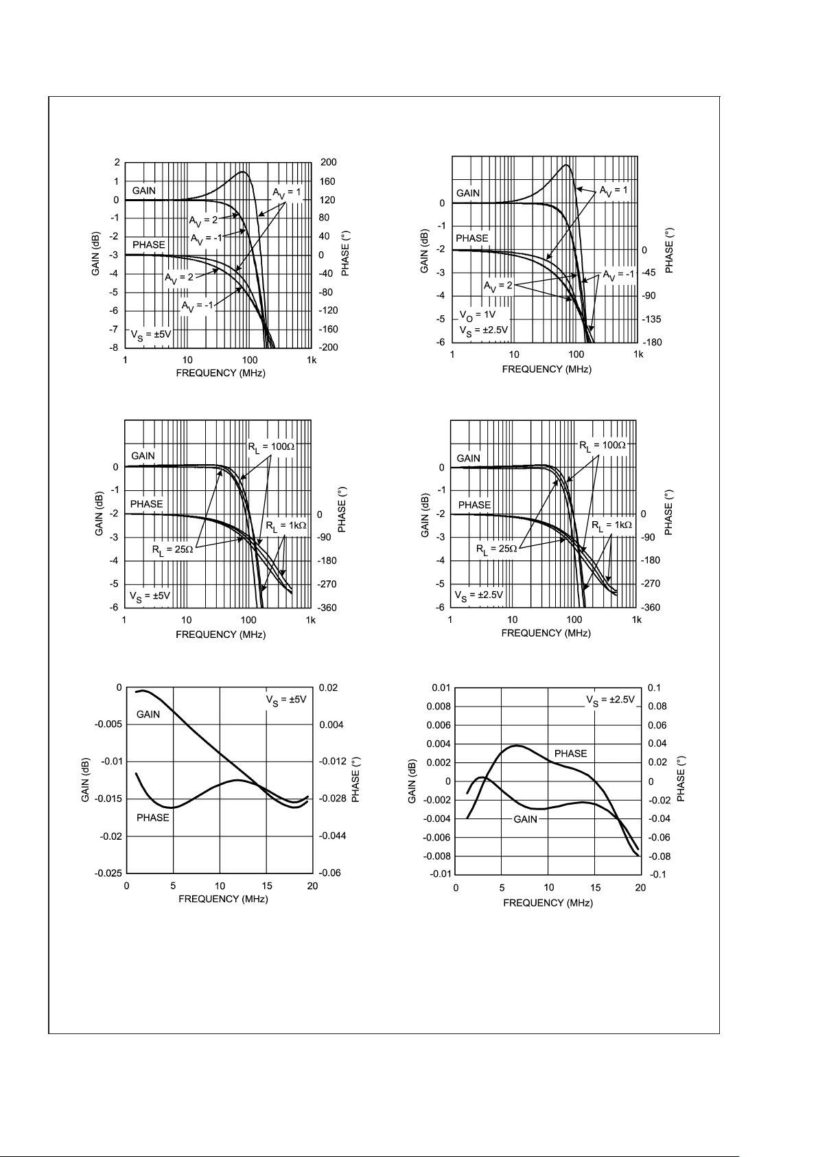
Typical Performance Characteristics (A
V
= +2, RL= 100Ω, Unless Specified).
Frequency Response vs. Gain Frequency Response
20040106
20040123
Frequency Response R
L
Frequency Response vs. R
L
20040125
20040124
Gain Flatness & Linear Phase Gain Flatness & Linear Phase
20040107
20040122
LMH6718
www.national.com5
Page 6

Typical Performance Characteristics (A
V
= +2, RL= 100Ω, Unless Specified). (Continued)
Frequency Response vs. V
O(AV
= 2) Frequency Response vs. VO(AV=2)
20040102
20040101
Frequency Response vs. VO(AV= 1) Frequency Response vs. VO(AV=1)
20040129
20040126
Frequency Response vs. VO(AV= -1) Frequency Response vs. VO(AV= -1)
20040128
20040127
LMH6718
www.national.com 6
Page 7

Typical Performance Characteristics (A
V
= +2, RL= 100Ω, Unless Specified). (Continued)
PSRR & CMRR PSRR & CMRR
20040131 20040130
2nd & 3rd Harmonic Distortion vs. Frequency 2nd & 3rd Harmonic Distortion vs. Frequency
20040113
20040109
2nd & 3rd Harmonic Distortion RL=25Ω 2nd & 3rd Harmonic Distortion RL=25Ω
20040114
20040115
LMH6718
www.national.com7
Page 8

Typical Performance Characteristics (A
V
= +2, RL= 100Ω, Unless Specified). (Continued)
2nd & 3rd Harmonic Distortion R
L
= 100Ω 2nd & 3rd Harmonic Distortion RL= 100Ω
20040110
20040111
2nd & 3rd Harmonic Distortion RL=1kΩ 2nd & 3rd Harmonic Distortion RL=1kΩ
20040112
20040108
Pulse Response Pulse Response
20040119
20040118
LMH6718
www.national.com 8
Page 9

Typical Performance Characteristics (A
V
= +2, RL= 100Ω, Unless Specified). (Continued)
Closed Loop Output Resistance Closed Loop Output Resistance
20040121 20040120
IBN&VIOvs. Temperature IBN&VIOvs. Temperature
20040134 20040133
Settling Time vs. Accuracy Channel Matching
20040161
20040103
LMH6718
www.national.com9
Page 10

Typical Performance Characteristics (A
V
= +2, RL= 100Ω, Unless Specified). (Continued)
Differential Gain & Phase Input Referred Crosstalk
20040165
20040132
Application Section
LMH6718 OPERATION
The LMH6718 is a current feedback buffer fabricated in an
advanced complementary bipolar process. The LMH6718
operates from a single 5V supply or dual
±
5V supplies.
Operating from a single 5V supply, the LMH6718 has the
following features:
•
Gains of±1, −1, and 2V/V are achievable without external resistors
•
Provides 170mA of output current
•
Offers low −88/−91dBc 2nd & 3rd harmonic distortion
•
Provides BW>110MHz
The LMH6718 performance is further enhanced in
±
5V sup-
ply applications as indicated in the
±
5V Electrical Charac-
teristics table and the
±
5V Typical Performance plots.
LMH6718 DESIGN INFORMATION
CLOSED LOOP GAIN SELECTION
The LMH6718 is a current feedback op amp with R
F=RG
=
1kΩ on chip (in the package). Select from three closed loop
gains without using any external gain or feedback resistors.
Implement gains of +2, +1, and −1V/V by connecting pins 2
and 3 (or 5 and 6) as described in the chart below.
Gain A
V
Input Connections
Non-Inverting (pins 3,5)Inverting (pins 2, 6)
−1V/V ground input signal
+1V/V input signal NC (open)
+2V/V input signal ground
The gain accuracy of the LMH6718 is excellent and stable
over temperature change. The internal gain setting resistors,
R
F
and RGare poly silicon resistors. Although their absolute
values change with processing and temperature, their ratio
(R
F/RG
) remains constant. If an external resistor is used in
series with R
G
, gain accuracy over temperature will suffer.
SINGLE SUPPLY OPERATION (V
CC
= +5V, VEE= GND)
The specifications given in the +5V Electrical Characteristics table for single supply operation are measured with a
common mode voltage (V
CM
) of 2.5V. VCMis the voltage
around which the inputs are applied and the output voltages
are specified.
Operating from a single +5V supply, the Common Mode
Voltage Range (CMVR) of the LMH6718 is typically +0.8V to
+4.2V. The typical output range with R
L
= 100Ω is +1.0V to
+4.0V.
For single supply DC coupled operation, keep input signal
levels above 0.8V DC, AC coupling and level shifting the
signal are recommended. The non-inverting and inverting
configurations for both input conditions are illustrated in the
following 2 sections.
DC COUPLED SINGLE SUPPLY OPERATION
Figure 1, Figure 2, and Figure 3 on the following page, show
the recommended configurations for input signals that remain above 0.8V DC.
20040139
FIGURE 1. DC Coupled, AV= −1V/V Configuration
LMH6718
www.national.com 10
Page 11

Application Section (Continued)
AC COUPLED SINGLE SUPPLY OPERATION
Figure 4, Figure 5, and Figure 6 show possible non-inverting
and inverting configurations for input signals that go below
0.8V DC.
The input is AC coupled to prevent the need for level shifting
the input signal at the source. The resistive voltage divider
biases the non-inverting input to V
CC
÷ 2 = 2.5V (For VCC=
+5V)
DUAL SUPPLY OPERATION
The LMH6718 operates on dual supplies as well as single
supplies. The non-inverting and inverting configurations are
shown in Figure 7, Figure 8, and Figure 9.
20040140
FIGURE 2. DC Coupled, AV= +1V/V Configuration
20040141
FIGURE 3. DC Coupled, AV= +2V/V Configuration
20040142
FIGURE 4. AC Coupled, AV= −1V/V Configuration
20040143
FIGURE 5. AC Coupled, AV= +1V/V Configuration
20040144
FIGURE 6. AC Coupled, AV= +2V/V Configuration
LMH6718
www.national.com11
Page 12

Application Section (Continued)
LOAD TERMINATION
The LMH6718 can source and sink nearly equal amounts of
current.
DRIVING CABLES AND CAPACITIVE LOADS
When driving cables, double termination is used to prevent
reflections. For capacitive load applications, a small series
resistor at the output of the LMH6718 will improve stability
and settling performance. The Suggested R
S
vs. CLplot,
shown below in Figure 10, gives the recommended series
resistance value for optimum flatness at various capacitive
loads.
TRANSMISSION LINE MATCHING
One method for matching the characteristic impedance (Z
O
)
of a transmission line or cable is to place the appropriate
resistor at the input or output of the amplifier. Figure 11
shows typical inverting and non-inverting circuit configurations for matching transmission lines.
Non-Inverting gain applications:
•
Connect pin 2 as indicated in the table in the Closed
Loop Gain Selection section.
•
Make R1,R2,R6, and R7equal to ZO.
•
Use R3to isolate the amplifier from reactive loading
caused by the transmission line, or by parasitics.
Inverting gain applications:
•
Connect R3directly to ground.
•
Make the resistors R4,R6, and R7equal to ZO.
•
Make R5\ Rg=ZO.
The input and output matching resistors attenuate the signal
by a factor of 2, therefore additional gain is needed. Use C6
to match the output transmission line over a greater frequency range. C6 compensates for the increase of the amplifier’s output impedance with frequency.
20040145
FIGURE 7. Dual Supply, AV= −1V/V Configuration
20040146
FIGURE 8. Dual Supply, AV= +1V/V Configuration
20040147
FIGURE 9. Dual Supply, AV= +2V/V Configuration
20040166
FIGURE 10. Suggested RSvs. C
L
LMH6718
www.national.com 12
Page 13

Application Section (Continued)
POWER DISSIPATION
Follow these steps to determine the power consumption of
the LMH6718:
1. Calculate the quiescent (no-load) power: P
amp=ICC
(VCC−VEE)
2. Calculate the RMS power at the output stage: P
O
=(V
CC
−V
LOAD
)(I
LOAD
), where V
LOAD
and I
LOAD
are the voltage and
current across the external load.
3. Calculate the total RMS power: P
t=Pamp+PO
. The maximum power that the SOIC, package can dissipate at a given
temperature is illustrated in Figure 12. The power derating
curve for any LMH6718 package can be derived by utilizing
the following equation:
where
T
amb
= Ambient temperature (˚C)
θ
JA
= Thermal resistance, from junction to ambient, for a
given package (˚C/W)
LAYOUT CONSIDERATIONS
A proper printed circuit layout is essential for achieving high
frequency performance. National provides evaluation boards
for the LMH6718 (CLC730036-SOIC) and suggests their use
as a guide for high frequency layout and as an aid for device
testing and characterization.
General layout and supply bypassing play major roles in high
frequency performance. Follow the steps below as a basis
for high frequency layout:
•
Include 6.8µF tantalum and 0.1µF ceramic capacitors on
both supplies.
•
Place the 6.8µF capacitors within 0.75 inches of the
power pins.
•
Place the 0.1µF capacitors less than 0.1 inches from the
power pins.
•
Remove the ground plane under and around the part,
especially near the input and output pins to reduce parasitic capacitance.
•
Minimize all trace lengths to reduce series inductances.
•
Use flush-mount printed circuit board pins for prototyping,
never use high profile DIP sockets.
EVALUATION BOARD INFORMATION
A datasheet is available for the CLC730036 evaluation
board. The evaluation board data sheets provide:
•
Evaluation board schematics
•
Evaluation board layouts
•
General information about the boards
The evaluation boards are designed to accommodate dual
supplies. The boards can be modified to provide single
supply operation. For best performance; 1) do not connect
the unused supply, 2) ground the unused supply pin.
SPECIAL EVALUATION BOARD CONSIDERATION FOR
THE LMH6718
To optimize off-isolation of the LMH6718, cut the R
f
trace on
the CLC730036 evaluation boards. This cut minimizes capacitive feedthrough between the input and the output. Fig-
ure 13 shows where to cut both evaluation boards for improved off-isolation.
20040149
FIGURE 11. Transmission Line Matching
20040163
FIGURE 12. Power Derating Curve
20040152
FIGURE 13. Evaluation Board Changes
LMH6718
www.national.com13
Page 14

Application Circuits
SINGLE SUPPLY CABLE DRIVER
Figure 14 below shows the LMH6718 driving 10m of 75Ω
coaxial cable. The LMH6718 is set for a gain of +2V/V to
compensate for the divide-by-two voltage drop at V
O
. The
response after 10m of cable is illustrated in Figure 15
DIFFERENTIAL LINE DRIVER WITH LOAD IMPEDANCE
CONVERSION
The circuit shown in Figure 16, operates as a differential line
driver. The transformer converts the load impedance to a
value that best matches the LMH6718’s output capabilities.
The single-ended input signal is converted to a differential
signal by the LMH6718. The line’s characteristic impedance
is matched at both the input and the output. The schematic
shows Unshielded Twisted Pair for the transmission line;
other types of lines can also be driven.
Set up the LMH6718 as a difference amplifier:
•
Set the Channel 1 amplifier to a gain of +1V/V
•
Set the Channel 2 amplifier to a gain of −1V/V
Make the best use of the LMH6718’s output drive capability
as follows:
where Reqis the transformed value of the load impedance,
V
max
is the output Voltage Range, and I
max
is the maximum
Output Current.
Match the line’s characteristic impedance:
Select the transformer so that it loads the line with a value
very near Z
O
over frequency range. The output impedance
of the LMH6718 also affects the match. With an ideal transformer we obtain:
where ZO(6718)(jω) is the output impedance of the
LMH6718 and |Z
O
(6718)(jω)|<<Rm.
The load voltage and current will fall in the ranges:
The LMH6718’s high output drive current and low distortion
make it a good choice for this application.
20040153
FIGURE 14. Single Supply Cable Driver
20040154
FIGURE 15. Response After 10m of Cable
20040155
FIGURE 16. Differential Line Driver with Load
Impedance Conversion
LMH6718
www.national.com 14
Page 15

Application Circuits (Continued)
DIFFERENTIAL INPUT/DIFFERENTIAL OUTPUT AMPLIFIER
below illustrates a differential input/differential output configuration. The bypass capacitors are the only external components
required.
20040160
FIGURE 17. Differential Input/Differential Output Amplifier
LMH6718
www.national.com15
Page 16

Physical Dimensions inches (millimeters)
unless otherwise noted
8-Pin SOIC
NS Package Number M08A
LIFE SUPPORT POLICY
NATIONAL’S PRODUCTS ARE NOT AUTHORIZED FOR USE AS CRITICAL COMPONENTS IN LIFE SUPPORT
DEVICES OR SYSTEMS WITHOUT THE EXPRESS WRITTEN APPROVAL OF THE PRESIDENT AND GENERAL
COUNSEL OF NATIONAL SEMICONDUCTOR CORPORATION. As used herein:
1. Life support devices or systems are devices or
systems which, (a) are intended for surgical implant
into the body, or (b) support or sustain life, and
whose failure to perform when properly used in
accordance with instructions for use provided in the
labeling, can be reasonably expected to result in a
significant injury to the user.
2. A critical component is any component of a life
support device or system whose failure to perform
can be reasonably expected to cause the failure of
the life support device or system, or to affect its
safety or effectiveness.
National Semiconductor
Americas Customer
Support Center
Email: new.feedback@nsc.com
Tel: 1-800-272-9959
National Semiconductor
Europe Customer Support Center
Fax: +49 (0) 180-530 85 86
Email: europe.support@nsc.com
Deutsch Tel: +49 (0) 69 9508 6208
English Tel: +44 (0) 870 24 0 2171
Français Tel: +33 (0) 1 41 91 8790
National Semiconductor
Asia Pacific Customer
Support Center
Fax: 65-6250 4466
Email: ap.support@nsc.com
Tel: 65-6254 4466
National Semiconductor
Japan Customer Support Center
Fax: 81-3-5639-7507
Email: nsj.crc@jksmtp.nsc.com
Tel: 81-3-5639-7560
www.national.com
LMH6718 Dual, High Output, Programmable Gain Buffer
National does not assume any responsibility for use of any circuitry described, no circuit patent licenses are implied and National reserves the right at any time without notice to change said circuitry and specifications.
 Loading...