

Page 1
查询LMH6702供应商
LMH6702
Ultra Low Distortion, Wideband Op Amp
LMH6702 Ultra Low Distortion, Wideband Op Amp
June 2003
General Description
The LMH6702 is a very wideband, DC coupled monolithic
operational amplifier designed specifically for wide dynamic
range systems requiring exceptional signal fidelity. Benefiting from National’s current feedback architecture, the
LMH6702 offers unity gain stability at exceptional speed
without need for external compensation.
With its 720MHz bandwidth (A
distortion levels through 60MHz (R
input referred noise and 12.5mA supply current, the
LMH6702 is the ideal driver or buffer for high-speed flash
A/D and D/A converters.
Wide dynamic range systems such as radar and communication receivers, requiring a wideband amplifier offering exceptional signal purity, will find the LMH6702’s low input
referred noise and low harmonic and intermodulation distortion make it an attractive high speed solution.
The LMH6702 is constructed using National’s VIP10
plimentary bipolar process and National’s proven current
feedback architecture. The LMH6702 is available in SOIC
and SOT23-5 packages.
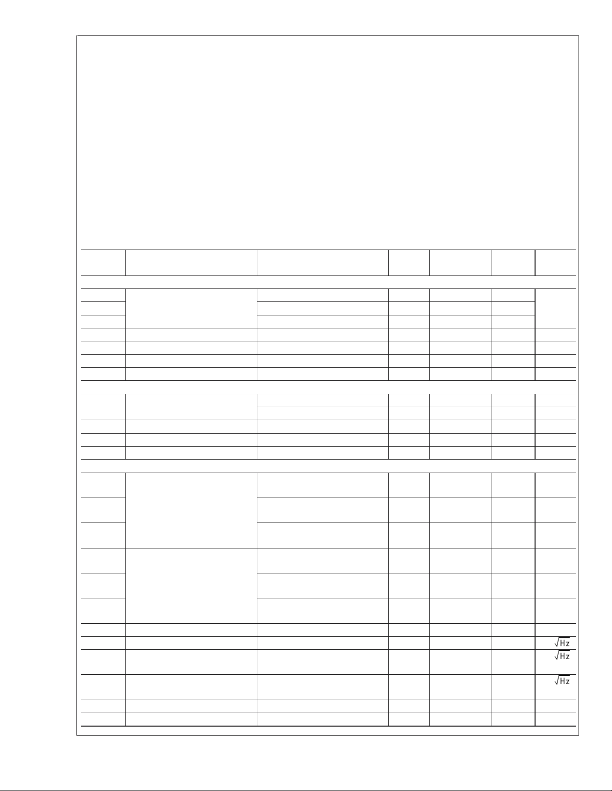
Inverting Frequency Response Harmonic Distortion vs. Load and Frequency
= 2V/V, VO=2VPP), 10-bit
V
= 100Ω), 1.83nV/
L
™
com-
Features
VS=±5V, TA= 25˚C, AV= +2V/V, RL= 100Ω,V
Typical unless Noted:
nd/3rd
n 2
n −3dB Bandwidth (V
n Low noise 1.83nV/
n Fast settling to 0.1% 13.4ns
n Fast slew rate 3100V/µs
n Supply current 12.5mA
n Output current 80mA
n Low Intermodulation Distortion (75MHz) −67dBc
n Improved Replacement for CLC409 and CLC449
Harmonics (5MHz, SOT23-5) −100/−96dBc
=2VPP) 720MHz
OUT
OUT
=2VPP,
Applications
n Flash A/D driver
n D/A transimpedance buffer
n Wide dynamic range IF amp
n Radar/communication receivers
n Line driver
n High resolution video
20039002
© 2003 National Semiconductor Corporation DS200390 www.national.com
20039007
Page 2
Absolute Maximum Ratings (Note 1)
If Military/Aerospace specified devices are required,
please contact the National Semiconductor Sales Office/
LMH6702
Distributors for availability and specifications.
V
S
I
OUT
Common Mode Input Voltage V
Maximum Junction Temperature +150˚C
Storage Temperature Range −65˚C to +150˚C
Soldering Information
Infrared or Convection (20 sec.) 235˚C
Wave Soldering (10 sec.) 260˚C
±
6.75V
(Note 3)
−
to V
+
Human Body Model 2000V
Machine Model 200V
Storage Temperature Range −65˚C to +150˚C
Operating Ratings (Note 1)
Thermal Resistance
Package (θ
8-Pin SOIC 75˚C/W 160˚C/W
5-Pin SOT23 120˚C/W 187˚C/W
Operating Temperature −40˚C to +85˚C
Nominal Supply Voltage
)(θJA)
JC
±
5V to±6V
ESD Tolerance (Note 4)
Electrical Characteristics (Note 2)
AV= +2, VS=±5V, RL= 100Ω,RF= 237Ω; unless specified
Symbol Parameter Conditions Min
(Note 6)
Frequency Domain Performance
SSBW
SSBW
GF
0.1dB
-3dB Bandwidth V
LG
LG
HG
0.1dB Gain Flatness V
=2V
OUT
V
OUT
V
OUT
OUT
PP
=4V
PP
=2VPP,AV= +10 140
=2V
PP
LPD Linear Phase Deviation DC to 100MHz 0.09 deg
DG Differential Gain R
DP Differential Phase R
=150Ω, 3.58MHz/4.43MHz 0.024/0.021 %
L
= 150Ω, 3.58MHz/4.43MHz 0.004/0.007 deg
L
Time Domain Response
TRS/TRL Rise and Fall Time 2V Step 0.87/0.77 ns
6V Step 1.70/1.70 ns
OS Overshoot 2V Step 0 %
SR Slew Rate 6V
T
s
Settling Time to 0.1% 2V Step 13.4 ns
, 40% to 60% (Note 5) 3100 V/µs
PP
Distortion And Noise Response
HD2L 2
nd
Harmonic Distortion 2VPP, 5MHz (Note 9)
(SOT23-5/SOIC)
HD2 2VPP, 20MHz (Note 9)
(SOT23-5/SOIC)
HD2H 2V
, 60MHz (Note 9)
PP
(SOT23-5/SOIC)
rd
HD3L 3
Harmonic Distortion 2VPP, 5MHz (Note 9)
(SOT23-5/SOIC)
HD3 2VPP, 20MHz (Note 9)
(SOT23-5/SOIC)
HD3H 2V
, 60MHz (Note 9)
PP
(SOT23-5/SOIC)
OIM3 IMD 75MHz, PO= 10dBm/ tone −67 dBc
V
N
I
N
Input Referred Voltage Noise
Input Referred Inverting Noise
>
1MHz 1.83 nV/
>
1MHz 18.5 pA/
Current
I
NN
Input Referred Non-Inverting
>
1MHz 3.0 pA/
Noise Current
SNF Total Input Noise Floor
>
1MHz −158 dBm
INV Total Integrated Input Noise 1MHz to 150MHz 35 µV
Typ
(Note 6)
Max
(Note 6)
720
480
120 MHz
−100/ −87 dBc
−79/ −72 dBc
−63/ −64 dBc
−96/ −98 dBc
−88/ −82 dBc
−70/ −65 dBc
Units
MHzLSBW
1Hz
www.national.com 2
Page 3
Electrical Characteristics (Note 2) (Continued)
AV= +2, VS=±5V, RL= 100Ω,RF= 237Ω; unless specified
Symbol Parameter Conditions Min
(Note 6)
Static, DC Performance
V
DV
IO
IO
Input Offset Voltage
Input Offset Voltage Average
(Note 8) −13 µV/˚C
Drift
I
DI
I
DI
BN
BN
BI
BI
Input Bias Current Non-Inverting (Note 7) −6
Input Bias Current Average Drift Non-Inverting (Note 8) +40 nA/˚C
Input Bias Current Inverting (Note 7) −8
Input Bias Current Average Drift Inverting (Note 8) −10 nA/˚C
PSRR Power Supply Rejection Ratio DC 47
45
CMRR Common Mode Rejection Ration DC 45
44
I
CC
Supply Current RL=
∞
11.0
10.0
Miscellaneous Performance
R
IN
C
IN
R
OUT
V
OL
CMIR Input Voltage Range Common Mode
I
O
Note 1: Absolute Maximum Ratings indicate limits beyond which damage to the device may occur. Operating Ratings indicate conditions for which the device is
intended to be functional, but specific performance is not guaranteed. For guaranteed specifications, see the Electrical Characteristics tables.
Note 2: Electrical Table values apply only for factory testing conditions at the temperature indicated. Factory testing conditions result in very limited self-heating of
the device such that T
Min/Max ratings are based on production testing unless otherwise specified.
Note 3: The maximum output current (I
Note 4: Human body model: 1.5kΩ in series with 100pF. Machine model: 0Ω in series with 200pF.
Note 5: Slew Rate is the average of the rising and falling edges.
Note 6: Typical numbers are the most likely parametric norm. Bold numbers refer to over temperature limits.
Note 7: Negative input current implies current flowing out of the device.
Note 8: Drift determined by dividing the change in parameter at temperature extremes by the total temperature change.
Note 9: Harmonic distortion is strongly influenced by package type (SOT23-5 or SOIC). See Application Note section under "Harmonic Distortion" for more
information.
Input Resistance Non-Inverting 1.4 MΩ
Input Capacitance Non-Inverting 1.6 pF
Output Resistance Closed Loop 30 mΩ
Output Voltage Range RL= 100Ω
±
3.3
±
3.2
±
1.9
Output Current 50 80 mA
. No guarantee of parametric performance is indicated in the electrical tables under conditions of internal self-heating where T
J=TA
) is determined by device power dissipation limitations.
OUT
Typ
(Note 6)
±
1.0
Max
(Note 6)
±
4.5
±
6.0
±
15
±
21
±
30
±
34
52 dB
48 dB
12.5 16.1
17.5
±
3.5 V
±
2.2 V
Units
mV
µA
µA
mA
>
J
LMH6702
TA.
www.national.com3
Page 4
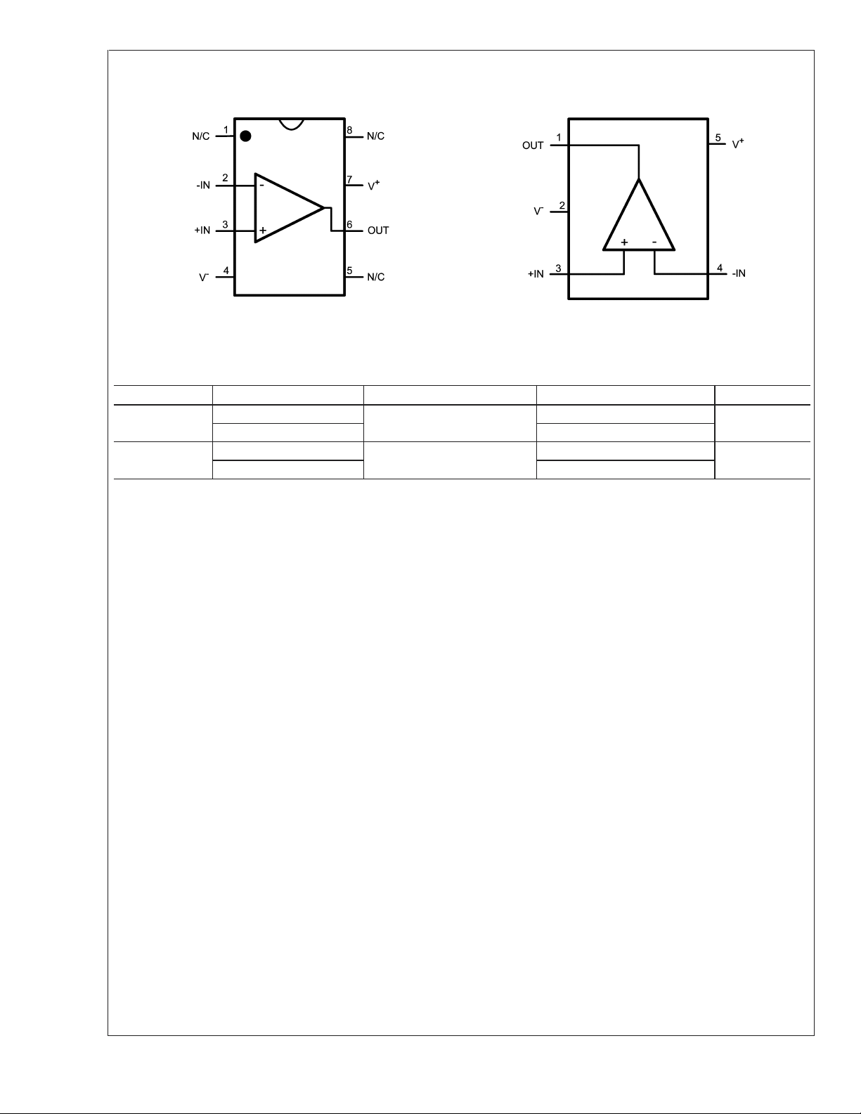
Connection Diagrams
LMH6702
8-Pin SOIC 5-Pin SOT23
Top View
20039024
Top View
Ordering Information
Package Part Number Package Marking Transport Media NSC Drawing
8-pin SOIC LMH6702MA LMH6702MA 95 Units/Rail
LMH6702MAX 2.5k Units Tape and Reel
5-Pin SOT23 LMH6702MF A83A 1k Units Tape and Reel MF05A
LMH6702MFX 3k Units Tape and Reel
20039025
M08A
www.national.com 4
Page 5

LMH6702
Typical Performance Characteristics (T
= 25˚C, VS=±5V, RL= 100Ω,Rf= 237Ω; Unless Speci-
A
fied).
Non-Inverting Frequency Response Inverting Frequency Response
20039001 20039002
Frequency Response for Various RL’s, AV= +2 Frequency Response for Various RL’s, AV=+4
Step Response, 2V
20039018 20039017
PP
20039005
Step Response, 6V
PP
20039006
www.national.com5
Page 6

Typical Performance Characteristics (T
Specified). (Continued)
LMH6702
Percent Settling vs. Time
20039020 20039007
2 Tone 3rd Order Spurious Level
(SOIC package) R
= 25˚C, VS=±5V, RL= 100Ω,Rf= 237Ω; Unless
A
Harmonic Distortion vs. Load and Frequency
(SOIC package)
and Settling Time vs. C
S
L
20039021
HD2 vs. Output Power (across 100Ω)
(SOIC package)
20039008 20039009
www.national.com 6
20039013
HD3 vs. Output Power (across 100Ω)
(SOIC package)
Page 7

LMH6702
Typical Performance Characteristics (T
= 25˚C, VS=±5V, RL= 100Ω,Rf= 237Ω; Unless
A
Specified). (Continued)
Input Offset for 3 Representative Units Inverting Input Bias for 3 Representative Units
20039014
Non-Inverting Input Bias for 3 Representative Units Noise
20039015
CMRR, PSRR, R
OUT
20039016 20039012
Transimpedance
20039019
20039011
www.national.com7
Page 8

Typical Performance Characteristics (T
Specified). (Continued)
LMH6702
DG/DP (NTSC) DG/DP (PAL)
= 25˚C, VS=±5V, RL= 100Ω,Rf= 237Ω; Unless
A
20039004
20039003
www.national.com 8
Page 9

Application Section
FEEDBACK RESISTOR
20039028
FIGURE 1. Recommended Non-Inverting Gain Circuit
monic distortion. For absolute minimum distortion levels, it is
also advisable to keep the supply decoupling currents
(ground connections to C
POS
, and C
in Figure 1 and
NEG
Figure 2) separate from the ground connections to sensitive
input circuitry (such as R
, and RINground connections).
G,RT
Splitting the ground plane in this fashion and separately
routing the high frequency current spikes on the decoupling
caps back to the power supply (similar to "Star Connection"
layout technique) ensures minimum coupling back to the
input circuitry and results in best harmonic distortion response (especially 2
nd
order distortion).
If this lay out technique has not been observed on a particular application board, designer may actually find that supply
decoupling caps could adversely affect HD2 performance by
increasing the coupling phenomenon already mentioned.
Figure 3 below shows actual HD2 data on a board where the
ground plane is "shared" between the supply decoupling
capacitors and the rest of the circuit. Once these capacitors
are removed, the HD2 distortion levels reduce significantly,
especially between 10MHz-20MHz, as shown in Figure 3
below:
LMH6702
20039027
FIGURE 2. Recommended Inverting Gain Circuit
The LMH6702 achieves its excellent pulse and distortion
performance by using the current feedback topology. The
loop gain for a current feedback op amp, and hence the
frequency response, is predominantly set by the feedback
resistor value. The LMH6702 is optimized for use with a
237Ω feedback resistor. Using lower values can lead to
excessive ringing in the pulse response while a higher value
will limit the bandwidth. Application Note OA-13 discusses
this in detail along with the occasions where a different R
might be advantageous.
HARMONIC DISTORTION
The LMH6702 has been optimized for exceptionally low
harmonic distortion while driving very demanding resistive or
capacitive loads. Generally, when used as the input amplifier
to very high speed flash ADCs, the distortions introduced by
the converter will dominate over the low LMH6702 distortions shown in the Typical Performance Characteristics section. The capacitor C
1 and Figure 2, is critical to achieving the lowest 2
, shown across the supplies in Figure
SS
nd
har-
20039022
FIGURE 3. Decoupling Current Adverse Effect on a
Board with Shared Ground Plane
At these extremely low distortion levels, the high frequency
behavior of decoupling capacitors themselves could be significant. In general, lower value decoupling caps tend to
have higher resonance frequencies making them more effective for higher frequency regions. A particular application
board which has been laid out correctly with ground returns
"split" to minimize coupling, would benefit the most by having
low value and higher value capacitors paralleled to take
advantage of the effective bandwidth of each and extend low
F
distortion frequency range.
Another important variable in getting the highest fidelity sig-
nal from the LMH6702 is the package itself. As already
noted, coupling between high frequency current transients
on supply lines and the device input can lead to excess
harmonic distortion. An important source of this coupling is in
fact through the device bonding wires. A smaller package, in
general, will have shorter bonding wires and therefore lower
coupling. This is true in the case of the SOT23-5 compared
to the SOIC package where a marked improvement in HD
can be measured in the SOT23-5 package. Figure 4 below
shows the HD comparing SOT23-5 to SOIC package:
www.national.com9
Page 10

Application Section (Continued)
LMH6702
CAPACITIVE LOAD DRIVE
Figure 5 shows a typical application using the LMH6702 to
drive an ADC.
20039029
20039023
FIGURE 4. SOIC and SOT23-5 Packages Distortion
Terms Compared
The LMH6702 data sheet shows both SOT23 and SOIC data
in the Electrical Characteristic section to aid in selecting the
right package. The Typical Performance Characteristics section shows SOIC package plots only.
rd
2-TONE 3
ORDER INTERMODULATION
The 2-tone, 3rd order spurious plot shows a relatively constant difference between the test power level and the spurious level with the difference depending on frequency. The
LMH6702 does not show an intercept type performance,
(where the relative spurious levels change at a 2X rate vs.
the test tone powers), due to an internal full power bandwidth
enhancement circuit that boosts the performance as the
output swing increases while dissipating negligible quiescent
power under low output power conditions. This feature enhances the distortion performance and full power bandwidth
to match that of much higher quiescent supply current parts.
FIGURE 5. Input Amplifier to ADC
The series resistor, R
, between the amplifier output and the
S
ADC input is critical to achieving best system performance.
This load capacitance, if applied directly to the output pin,
can quickly lead to unacceptable levels of ringing in the
pulse response. The plot of "R
and Settling Time vs. CL"in
S
the Typical Performance Characteristics section is an excellent starting point for selecting R
. The value derived in that
S
plot minimizes the step settling time into a fixed discrete
capacitive load with the output driving a very light resistive
load (1kΩ). Sensitivity to capacitive loading is greatly reduced once the output is loaded more heavily. Therefore, for
cases where the output is heavily loaded, R
value may be
S
reduced. The exact value may best be determined experimentally for these cases.
In applications where the LMH6702 is replacing the CLC409,
care must be taken when the device is lightly loaded and
some capacitance is present at the output. Due to the much
higher frequency response of the LMH6702 compared to the
CLC409, there could be increased susceptibility to low value
output capacitance (parasitic or inherent to the board layout
or otherwise being part of the output load). As already mentioned, this susceptibility is most noticeable when the
LMH6702’s resistive load is light. Parasitic capacitance can
be minimized by careful lay out. Addition of an output snubber R-C network will also help by increasing the high frequency resistive loading.
Referring back to Figure 5, it must be noted that several
additional constraints should be considered in driving the
capacitive input of an ADC. There is an option to increase
, band-limiting at the ADC input for either noise or Nyquist
R
S
band-limiting purposes. Increasing R
too much, however,
S
can induce an unacceptably large input glitch due to switching transients coupling through from the "convert" signal.
Also, C
is oftentimes a voltage dependent capacitance.
IN
This input impedance non-linearity will induce distortion
terms that will increase as R
adjustments up or down from the recommended R
is increased. Only slight
S
S
value
should therefore be attempted in optimizing system performance.
www.national.com 10
Page 11

Application Section (Continued)
DC ACCURACY AND NOISE
Example below shows the output offset computation equation for the non-inverting configuration using the typical bias
current and offset specifications for A
Output Offset : V
=(±IBN·R
O
IN
Where RINis the equivalent input impedance on the noninverting input.
Example computation for A
=(±6µA · 25Ω±1mV) (1 + 237/237)±8µA · 237 =
V
O
±
4.20mV
= +2, RF= 237Ω,RIN=25Ω:
V
A good design, however, should include a worst case calculation using Min/Max numbers in the data sheet tables, in
order to ensure "worst case" operation.
Further improvement in the output offset voltage and drift is
possible using the composite amplifiers described in Application Note OA-7. The two input bias currents are physically
unrelated in both magnitude and polarity for the current
feedback topology. It is not possible, therefore, to cancel
their effects by matching the source impedance for the two
inputs (as is commonly done for matched input bias current
devices).
The total output noise is computed in a similar fashion to the
output offset voltage. Using the input noise voltage and the
=+2:
V
±
VIO)(1+RF/RG)±IBI·R
LMH6702
two input noise currents, the output noise is developed
through the same gain equations for each term but combined as the square root of the sum of squared contributing
elements. See Application Note OA-12 for a full discussion of
noise calculations for current feedback amplifiers.
F
PRINTED CIRCUIT LAYOUT
Generally, a good high frequency layout will keep power
supply and ground traces away from the inverting input and
output pins. Parasitic capacitances on these nodes to
ground will cause frequency response peaking and possible
circuit oscillations (see Application Note OA-15 for more
information). National Semiconductor suggests the following
evaluation boards as a guide for high frequency layout and
as an aid in device testing and characterization:
Device Package Evaluation Board
Part Number
LMH6702MF SOT23-5 CLC730216
LMH6702MA SOIC CLC730227
These free evaluation boards are shipped when a device
sample request is placed with National Semiconductor.
www.national.com11
Page 12

Physical Dimensions inches (millimeters)
unless otherwise noted
LMH6702
8-Pin SOIC
NS Package Number M08A
5-Pin SOT23
NS Package Number MA05A
www.national.com 12
Page 13

Notes
LMH6702 Ultra Low Distortion, Wideband Op Amp
LIFE SUPPORT POLICY
NATIONAL’S PRODUCTS ARE NOT AUTHORIZED FOR USE AS CRITICAL COMPONENTS IN LIFE SUPPORT
DEVICES OR SYSTEMS WITHOUT THE EXPRESS WRITTEN APPROVAL OF THE PRESIDENT AND GENERAL
COUNSEL OF NATIONAL SEMICONDUCTOR CORPORATION. As used herein:
1. Life support devices or systems are devices or
systems which, (a) are intended for surgical implant
into the body, or (b) support or sustain life, and
whose failure to perform when properly used in
accordance with instructions for use provided in the
2. A critical component is any component of a life
support device or system whose failure to perform
can be reasonably expected to cause the failure of
the life support device or system, or to affect its
safety or effectiveness.
labeling, can be reasonably expected to result in a
significant injury to the user.
National Semiconductor
Americas Customer
Support Center
Email: new.feedback@nsc.com
Tel: 1-800-272-9959
www.national.com
National does not assume any responsibility for use of any circuitry described, no circuit patent licenses are implied and National reserves the right at any time without notice to change said circuitry and specifications.
National Semiconductor
Europe Customer Support Center
Fax: +49 (0) 180-530 85 86
Email: europe.support@nsc.com
Deutsch Tel: +49 (0) 69 9508 6208
English Tel: +44 (0) 870 24 0 2171
Français Tel: +33 (0) 1 41 91 8790
National Semiconductor
Asia Pacific Customer
Support Center
Email: ap.support@nsc.com
National Semiconductor
Japan Customer Support Center
Fax: 81-3-5639-7507
Email: jpn.feedback@nsc.com
Tel: 81-3-5639-7560
 Loading...