

Page 1
November 2002
LMH6682/6683
190MHz Single Supply, Dual and Triple Operational
Amplifiers
General Description
The LMH6682 and LMH6683 are high speed operational
amplifiers designed for use in modern video systems. These
single supply monolithic amplifiers extend National’s featurerich, high value video portfolio to include a dual and a triple
version. The important video specifications of differential
±
gain (
combined with an output drive current in each amplifier of
85mA make the LMH6682 and LMH6683 excellent choices
for a full range of video applications.
Voltage feedback topology in operational amplifiers assures
maximum flexibility and ease of use in high speed amplifier
designs. The LMH6682/83 is fabricated in National Semiconductor’s VIP10 process. This advanced process provides a
superior ratio of speed to quiescient current consumption
and assures the user of high-value amplifier designs. Advanced technology and circuit design enables in these amplifiers a −3db bandwidth of 190MHz, a slew rate of 940V/
µsec, and stability for gains of less than −1 and greater than
+2.
The input stage design of the LM6682/83 enables an input
signal range that extends below the negative rail. The output
stage voltage range reaches to within 0.8V of either rail
when driving a 2kΩ load. Other attractive features include
fast settling and low distortion. Other applications for these
amplifiers include servo control designs. These applications
are sensitive to amplifiers that exhibit phase reversal when
the inputs exceed the rated voltage range. The LMH6682/83
amplifiers are designed to be immune to phase reversal
when the specified input range is exceeded. See applications section. This feature makes for design simplicity and
flexibility in many industrial applications.
0.01% typ.) and differential phase (±0.08 degrees)
The LMH6682 dual operational amplifier is offered in miniature surface mount packages, SOIC-8, and MSOP-8. The
LMH6683 triple amplifier is offered in SOIC-14 and TSSOP-
14.
Features
VS=±5V, TA= 25˚C, RL= 100Ω, A = +2 (Typical values
unless specified)
n DG error 0.01%
n DP error 0.08˚
n −3dB BW (A = +2) 190MHz
n Slew rate (V
n Supply current 6.5mA/amp
n Output current +80/−90mA
n Input common mode voltage 0.5V beyond V
+
V
n Output voltage swing (RL=2kΩ) 0.8V from rails
n Input voltage noise (100KHz) 12nV/
=±5V) 940V/µs
S
Applications
n CD/DVD ROM
n ADC buffer amp
n Portable video
n Current sense buffer
n Portable communications
−
, 1.7V from
LMH6682/6683 190MHz Single Supply, Dual and Triple Operational Amplifiers
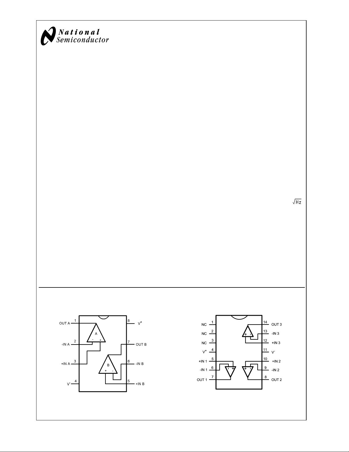
Connection Diagrams
SOIC-8/MSOP-8 (LMH6682) SOIC-14/TSSOP-14 (LMH6683)
Top View
20059002
© 2002 National Semiconductor Corporation DS200590 www.national.com
Top View
20059003
Page 2
Absolute Maximum Ratings (Note 1)
If Military/Aerospace specified devices are required,
Storage Temperature Range −65˚C to +150˚C
Junction Temperature (Note 7) +150˚C
please contact the National Semiconductor Sales Office/
Distributors for availability and specifications.
LMH6682/6683
ESD Tolerance
Human Body Model 2KV(Note 2)
Machine Model 200V (Note 3)
Differential
V
IN
Output Short Circuit Duration (Note 4), (Note 6)
Input Current
Supply Voltage (V
Voltage at Input/Output pins V
+-V−
) 12.6V
+
+0.8V, V−−0.8V
Soldering Information
±
±
10mA
2.5V
Operating Ratings (Note 1)
Supply Voltage (V
Operating Temperature Range
(Note 7) −40˚C to +85˚C
Package Thermal Resistance (Note 7)
SOIC-8 190˚C/W
MSOP-8 235˚C/W
SOIC-14 145˚C/W
TSSOP-14 155˚C/W
+–V−
) 3Vto12V
Infrared or Convection (20 sec.) 235˚C
Wave Soldering (10 sec.) 260˚C
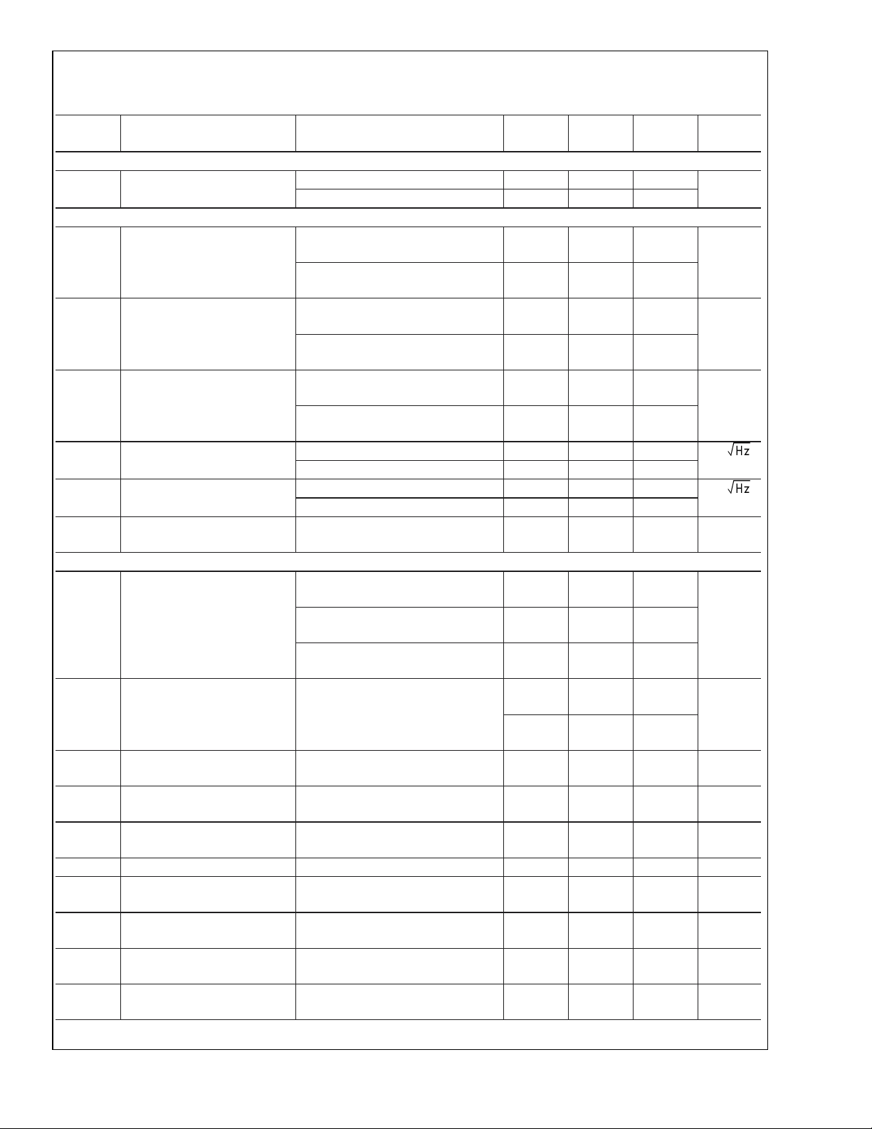
5V Electrical Characteristics
Unless otherwise specified, all limits guaranteed for at TJ= 25˚C, V+= 5V, V−= 0V, VO=VCM=V+/2, and RL= 100Ω to V+/2,
= 510Ω. Boldface limits apply at the temperature extremes.
R
F
Symbol Parameter Conditions Min
(Note 9)
SSBW −3dB BW A = +2, V
A = −1, V
GFP Gain Flatness Peaking A = +2, V
OUT
OUT
OUT
= 200mV
= 200mV
= 200mV
PP
PP
PP
DC to 100MHz
GFR Gain Flatness Rolloff A = +2, V
OUT
= 200mV
PP
DC to 100MHz
LPD 1˚ 1˚ Linear Phase Deviation A = +2, V
GF
0.1dB
0.1dB Gain Flatness A = +2,±0.1dB, V
FPBW Full Power −1dB Bandwidth A = +2, V
DG Differential Gain
NTSC 3.58MHz
DP Differential Phase
NTSC 3.58MHz
A = +2, R
Pos video only V
A = +2, R
Pos video only V
= 200mVPP,±1˚ 40 MHz
OUT
= 200mV
OUT
=2V
OUT
L
L
PP
= 150Ω to V+/2
=2V
CM
= 150Ω to V+/2
=2V
CM
PP
Time Domain Response
T
r/Tf
OS Overshoot A = +2, V
T
s
SR Slew Rate (Note 11) A = +2, V
Rise and Fall Time 20-80%, VO=1VPP,AV= +2 2.1
20-80%, V
=1VPP,AV=−1 2
O
= 100mV
O
PP
Settling Time VO=2VPP,±0.1%, AV=+2 49 ns
=3V
A = −1, V
OUT
OUT
=3V
PP
PP
Distortion and Noise Response
HD2 2
nd
Harmonic Distortion f = 5MHz, VO=2VPP, A = +2, RL=
2kΩ
f = 5MHz, V
=2VPP, A = +2, RL=
O
100Ω
HD3 3rdHarmonic Distortion f = 5MHz, VO=2VPP, A = +2, RL=
2kΩ
f = 5MHz, VO=2VPP, A = +2, RL=
100Ω
140 180
Typ
(Note 8)
Max
(Note 9)
180
2.1 dB
0.1 dB
25 MHz
110 MHz
0.03 %
0.05 deg
22 %
520
500
−60
−61
−77
−54
Units
MHz
ns
V/µs
dBc
dBc
www.national.com 2
Page 3
5V Electrical Characteristics (Continued)
Unless otherwise specified, all limits guaranteed for at TJ= 25˚C, V+= 5V, V−= 0V, VO=VCM=V+/2, and RL= 100Ω to V+/2,
= 510Ω. Boldface limits apply at the temperature extremes.
R
F
Symbol Parameter Conditions Min
(Note 9)
Distortion and Noise Response
THD Total Harmonic Distortion f = 5MHz, V
=2VPP, A = +2, RL=
O
2kΩ
f = 5MHz, VO=2VPP, A = +2, RL=
100Ω
e
n
Input Referred Voltage Noise f = 1kHz 17 nV/
f = 100kHz 12
i
n
Input Referred Current Noise f = 1kHz 8 pA/
f = 100kHz 3
CT Cross-Talk Rejection
(Amplifier)
f = 5MHz, A = +2, SND: R
F=RG
= 510Ω
RCV: R
= 100Ω
L
Static, DC Performance
A
VOL
CMVR Input Common-Mode Voltage
Large Signal Voltage Gain VO= 1.25V to 3.75V,
=2kΩ to V+/2
R
L
V
= 1.5V to 3.5V,
O
= 150Ω to V+/2
R
L
V
=2Vto3V,
O
=50Ω to V+/2
R
L
CMRR ≥ 50dB −0.2
Range
V
OS
TC V
Input Offset Voltage
Input Offset Voltage Average
OS
(Note 12)
Drift
I
B
TC
IB
I
OS
CMRR Common Mode Rejection
Input Bias Current (Note 10) −5 −20
Input Bias Current Drift 0.01 nA/˚C
Input Offset Current 50 300
Stepped from 0V to 3.0V 72 82 dB
V
CM
Ratio
+
+PSRR Positive Power Supply
= 4.5V to 5.5V, VCM=1V 70 76 dB
V
Rejection Ratio
I
S
Supply Current (per channel) No load 6.5 9
85 95
75 85
70 80
−0.1
3.0
2.8
Typ
(Note 8)
Max
(Note 9)
−60
−53
−77 dB
−0.5
3.3
±
1.1
±
2 µV/˚C
±
5
±
7
−30
500
11
Units
dBc
mV
mA
LMH6682/6683
dB
V
µA
nA
www.national.com3
Page 4
5V Electrical Characteristics (Continued)
Unless otherwise specified, all limits guaranteed for at TJ= 25˚C, V+= 5V, V−= 0V, VO=VCM=V+/2, and RL= 100Ω to V+/2,
= 510Ω. Boldface limits apply at the temperature extremes.
R
F
Symbol Parameter Conditions Min
LMH6682/6683
Miscellaneous Performance
V
I
I
R
C
R
O
OUT
SC
IN
IN
OUT
Output Swing
RL=2kΩ to V+/2 4.10
High
RL= 150Ω to V+/2 3.90
=75Ω to V+/2 3.75
R
L
Output Swing
RL=2kΩ to V+/2 800 920
Low
= 150Ω to V+/2 870 970
R
L
RL=75Ω to V+/2 885 1100
Output Current VO= 1V from either supply rail
Output Short Circuit Current
Sourcing to V+/2 −100
(Note 5), (Note 6), (Note 10)
+
Sinking from V
/2 100
Common Mode Input
Resistance
Common Mode Input
Capacitance
Output Resistance Closed
Loop
f = 1kHz, A = +2, RL=50Ω 0.02
f = 1MHz, A = +2, R
=50Ω 0.12
L
(Note 9)
3.8
3.70
3.50
±
40 +80/−75 mA
−80
80
Typ
(Note 8)
4.25
4.19
4.15
−155
220
3
1.6
Max
(Note 9)
1100
1200
1250
Units
V
mV
mA
MΩ
pF
Ω
±
5V Electrical Characteristics
Unless otherwise specified, all limits guaranteed for at TJ= 25˚C, V+= 5V, V−= −5V, VO=VCM= 0V, and RL= 100Ω to 0V,
= 510Ω. Boldface limits apply at the temperature extremes.
R
F
Symbol Parameter Conditions Min
(Note 9)
SSBW −3dB BW A = +2, V
A = −1, V
GFP Gain Flatness Peaking A = +2, V
OUT
OUT
OUT
= 200mV
= 200mV
= 200mV
PP
PP
PP
150 190
Typ
(Note 8)
Max
(Note 9)
190
1.7 dB
DC to 100MHz
GFR Gain Flatness Rolloff A = +2, V
OUT
= 200mV
PP
0.1 dB
DC to 100MHz
LPD 1˚ 1˚ Linear Phase Deviation A = +2, V
GF
0.1dB
0.1dB Gain Flatness A = +2,±0.1dB, V
FPBW Full Power −1dB Bandwidth A = +2, V
DG Differential Gain
A = +2, R
= 200mVPP,±1˚ 40 MHz
OUT
= 200mV
OUT
=2V
OUT
L
PP
= 150Ω to 0V 0.01 %
PP
25 MHz
120 MHz
NTSC 3.58MHz
DP Differential Phase
A = +2, RL= 150Ω to 0V 0.08 deg
NTSC 3.58MHz
Time Domain Response
T
r/Tf
OS Overshoot A = +2, V
T
s
Rise and Fall Time 20-80%, VO=1VPP,A=+2 1.9
20-80%, V
=1VPP,A=−1 2
O
= 100mV
O
PP
19 %
Settling Time VO=2VPP,±0.1%, A = +2 42 ns
Units
MHz
ns
www.national.com 4
Page 5
±
5V Electrical Characteristics (Continued)
Unless otherwise specified, all limits guaranteed for at TJ= 25˚C, V+= 5V, V−= −5V, VO=VCM= 0V, and RL= 100Ω to 0V,
= 510Ω. Boldface limits apply at the temperature extremes.
R
F
Symbol Parameter Conditions Min
(Note 9)
Typ
(Note 8)
Max
(Note 9)
Time Domain Response
SR Slew Rate (Note 11) A = +2, V
A = −1, V
OUT
OUT
=6V
=6V
PP
PP
940
900
Distortion and Noise Response
HD2 2
nd
Harmonic Distortion f = 5MHz, VO=2VPP, A = +2, RL=
−63
2kΩ
f = 5MHz, V
=2VPP, A = +2, RL=
O
−66
100Ω
HD3 3rdHarmonic Distortion f = 5MHz, VO=2VPP, A = +2, RL=
−82
2kΩ
f = 5MHz, VO=2VPP, A = +2, RL=
−54
100Ω
THD Total Harmonic Distortion f = 5MHz, V
=2VPP, A = +2, RL=
O
−63
2kΩ
f = 5MHz, V
=2VPP, A = +2, RL=
O
−54
100Ω
e
n
Input Referred Voltage Noise f = 1kHz 18 nV/
f = 100kHz 12
i
n
Input Referred Current Noise f = 1kHz 6 pA/
f = 100kHz 3
CT Cross-Talk Rejection
(Amplifier)
f = 5MHz, A = +2, SND: R
F=RG
= 510Ω
RCV: R
= 100Ω
L
−78 dB
Static, DC Performance
A
VOL
Large Signal Voltage Gain VO= −3.75V to 3.75V,
CMVR Input Common Mode Voltage
Range
=2kΩ to V+/2
R
L
V
= −3.5V to 3.5V,
O
= 150Ω to V+/2
R
L
V
= −3V to 3V,
O
=50Ω to V+/2
R
L
CMRR ≥ 50dB −5.2
87 100
80 90
75 85
−5.1
3.0
−5.5
3.3
2.8
V
OS
TC V
Input Offset Voltage
Input Offset Voltage Average
OS
(Note 12)
±
1
±
2 µV/˚C
±
5
±
7
Drift
I
B
Input Bias Current (Note 10) −5 −20
−30
TC
I
OS
IB
Input Bias Current Drift 0.01 nA/˚C
Input Offset Current 50 300
500
CMRR Common Mode Rejection
Stepped from −5V to 3.0V 75 84 dB
V
CM
Ratio
+PSRR Positive Power Supply
Rejection Ratio
−PSRR Negative Power Supply
Rejection Ratio
V+= 8.5V to 9.5V,
−
= −1V
V
−
V
= −4.5V to −5.5V,
+
=5V
V
75 82 dB
78 85 dB
LMH6682/6683
Units
V/µs
dBc
dBc
dBc
dB
V
mV
µA
nA
www.national.com5
Page 6
±
5V Electrical Characteristics (Continued)
Unless otherwise specified, all limits guaranteed for at TJ= 25˚C, V+= 5V, V−= −5V, VO=VCM= 0V, and RL= 100Ω to 0V,
= 510Ω. Boldface limits apply at the temperature extremes.
R
F
Symbol Parameter Conditions Min
LMH6682/6683
(Note 9)
Typ
(Note 8)
Max
(Note 9)
Static, DC Performance
I
S
Supply Current (per channel) No load 6.5 9.5
11
Miscellaneous Performance
V
O
Output Swing
High
RL=2kΩ to 0V 4.10
3.80
= 150Ω to 0V 3.90
R
L
4.25
4.20
3.70
RL=75Ω to 0V 3.75
4.18
3.50
Output Swing
Low
=2kΩ to 0V −4.19 −4.07
R
L
= 150Ω to 0V −4.05 −3.89
R
L
−3.80
−3.65
RL=75Ω to 0V −4.00 −3.70
−3.50
I
I
OUT
SC
Output Current VO= 1V from either supply rail
Output Short Circuit Current
Sourcing to 0V −120
(Note 5) , (Note 6),(Note 10)
Sinking from 0V 120
±
45 +85/−80 mA
−180
−100
230
100
R
IN
Common Mode Input
4
Resistance
C
IN
Common Mode Input
1.6
Capacitance
R
OUT
Note 1: Absolute maximum Ratings indicate limits beyond which damage to the device may occur. Operating Ratings indicate conditions for which the device is
intended to be functional, but specific performance is not guaranteed. For guaranteed specifications and the test conditions, see the Electrical Characteristics.
Note 2: Human body model, 1.5kΩ in series with 100pF.
Note 3: Machine Model, 0Ω in series with 200pF.
Note 4: Applies to both single-supply and split-supply operation. Continuous short circuit operation at elevated ambient temperature can result in exceeding the
maximum allowed junction temperature of 150˚C.
Note 5: Short circuit test is a momentary test. See next note.
Note 6: Output short circuit duration is infinite for V
Note 7: The maximum power dissipation is a function of T
P
D
Note 8: Typical values represent the most likely parametric norm.
Note 9: All limits are guaranteed by testing or statistical analysis.
Note 10: Positive current corresponds to current flowing into the device.
Note 11: Slew rate is the average of the rising and falling slew rates
Note 12: Offset Voltage average drift determined by dividing the change in V
Output Resistance Closed
Loop
=(T
J(MAX)-TA
)/ θJA. All numbers apply for packages soldered directly onto a PC board.
f = 1kHz, A = +2, RL=50Ω 0.02
f = 1MHz, A = +2, R
<
6V at room temperature and below. For V
S
, θJA, and TA. The maximum allowable power dissipation at any ambient temperature is
J(MAX)
=50Ω 0.12
L
>
6V, allowable short circuit duration is 1.5ms.
S
at temperature extremes into the total temperature change.
OS
Units
mA
V
mV
mA
MΩ
pF
Ω
www.national.com 6
Page 7

Typical Schematic
LMH6682/6683
20059001
Ordering Information
Package Part Number Package Marking Transport Media NSC Drawing
8-Pin SOIC LMH6682MA
LMH6682MAX 2.5k Units Tape and Reel
8-Pin MSOP LMH6682MM
LMH6682MMX 2.5k Units Tape and Reel
14-Pin SOIC LMH6683MA
LMH6683MAX 2.5k Units Tape and Reel
14-Pin
TSSOP
LMH6683MT
LMH6683MTX 2.5 Units Tape and Reel
LMH6682MA
A90A
LMH6683MA
LMH6683MT
95 Units/Rail
1k Units Tape and Reel
55 Units/Rail
94 Units/Rail
M08A
MUA08A
M14A
MTC14
www.national.com7
Page 8

Typical Performance Characteristics
At TA= 25˚C, V+= +5V, V−= −5V, RF= 510Ω for A = +2; unless otherwise specified.
Non-Inverting Frequency Response Inverting Frequency Response
LMH6682/6683
20059004 20059006
Non-Inverting Frequency Response for Various Gain Inverting Frequency Response for Various Gain
20059005
Non-Inverting Phase vs. Frequency for Various Gain Inverting Phase vs. Frequency for Various Gain
20059024 20059025
www.national.com 8
20059007
Page 9

Typical Performance Characteristics (Continued)
Open Loop Gain and Phase vs. Frequency Over
Open Loop Gain & Phase vs. Frequency
LMH6682/6683
Temperature
20059008
20059057
Non-Inverting Frequency Response Over Temperature Inverting Frequency Response Over Temperature
20059038 20059037
Gain Flatness 0.1dB Differential Gain & Phase for A = +2
20059009
20059013
www.national.com9
Page 10

Typical Performance Characteristics (Continued)
Transient Response Negative Transient Response Positive
LMH6682/6683
20059012 20059010
Noise vs. Frequency Noise vs. Frequency
20059039 20059020
Harmonic Distortion vs. V
www.national.com 10
OUT
20059045
Harmonic Distortion vs. V
OUT
20059044
Page 11

Typical Performance Characteristics (Continued)
LMH6682/6683
Harmonic Distortion vs. V
OUT
20059043 20059042
THD vs. for Various Frequencies
Harmonic Distortion vs. Frequency Crosstalk vs. Frequency
20059046
R
vs. Frequency IOSvs. V
OUT
20059021
Over Temperature
SUPPLY
20059014
20059023
www.national.com11
Page 12

Typical Performance Characteristics (Continued)
LMH6682/6683
V
vs. V
OS
VOSvs. V
@
−40˚C VOSvs. V
S
20059047 20059048
@
85˚C VOSvs. V
S
@
25˚C
S
@
125˚C
S
20059049 20059050
VOSvs. V
www.national.com 12
OUT
20059035 20059036
VOSvs. V
OUT
Page 13

Typical Performance Characteristics (Continued)
I
/Amp vs. V
SUPPLY
V
OUT
vs. I
CM
20059030 20059026
SOURCE
I
SUPPLY
/Amp vs. V
V
vs. I
OUT
LMH6682/6683
SUPPLY
SINK
20059031 20059033
V
OUT
vs. I
SOURCE
20059032 20059034
V
vs. I
OUT
SINK
www.national.com13
Page 14

Typical Performance Characteristics (Continued)
V
vs. V
OS
LMH6682/6683
CM
|IB|vs. V
S
20059028
Short Circuit I
SOURCE
vs. V
S
20059059
Short Circuit I
SINK
vs. V
Linearity Input vs. Output Linearity Input vs. Output
20059064
S
20059058
20059041 20059040
www.national.com 14
Page 15

Typical Performance Characteristics (Continued)
CMRR vs. Frequency PSRR vs. Frequency
LMH6682/6683
20059022
Small Signal Pulse Response for A = +2 Small Signal Pulse Response A = −1
20059015
Large Signal Pulse Response Large Signal Pulse Response
20059011
20059016
20059017
20059018
www.national.com15
Page 16

Applications Section
LARGE SIGNAL BEHAVIOR
Amplifying high frequency signals with large amplitudes (as
in video applications) has some special aspects to look after.
The bandwidth of the Op Amp for large amplitudes is less
LMH6682/6683
than the small signal bandwidth because of slew rate limitations. While amplifying pulse shaped signals the slew rate
properties of the OpAmp become more important at higher
amplitude ranges. Due to the internal structure of an Op Amp
the output can only change with a limited voltage difference
per time unit (dV/dt). This can be explained as follows: To
keep it simple, assume that an Op Amp consists of two parts;
the input stage and the output stage. In order to stabilize the
Op Amp, the output stage has a compensation capacitor in
its feedback path. This Miller C integrates the current from
the input stage and determines the pulse response of the Op
Amp. The input stage must charge/discharge the feedback
capacitor, as can be seen in Figure 1.
20059061
FIGURE 2.
This property of the LMH6682/83 guaranties a higher slew
rate at higher differential input voltages.
∆V/∆t=∆V*Gm/C (5)
In Figure 3 one can see that a higher transient voltage than
will lead to a higher slew rate.
20059060
FIGURE 1.
When a voltage transient is applied to the non inverting input
of the Op Amp, the current from the input stage will charge
the capacitor and the output voltage will slope up. The
overall feedback will subtract the gradually increasing output
voltage from the input voltage. The decreasing differential
input voltage is converted into a current by the input stage
(Gm).
I*∆t=C*∆V (1)
∆V/∆t = I/C (2)
I=∆V*Gm (3)
where I = current
t = time
C = capacitance
V = voltage
Gm = transconductance
Slew rate ∆V/∆t = volt/second
In most amplifier designs the current I is limited for high
differential voltages (Gm becomes zero). The slew rate will
than be limited as well:
∆V/∆t = Imax/C (4)
The LMH6682/83 has a different setup of the input stage. It
has the property to deliver more current to the output stage
when the input voltage is higher (class AB input). The current
into the Miller capacitor exhibits an exponential character,
while this current in other Op Amp designs reaches a saturation level at high input levels: (see Figure 2)
20059062
FIGURE 3.
HANDLING VIDEO SIGNALS
When handling video signals, two aspects are very important
especially when cascading amplifiers in a NTSC- or PAL
video system. A composite video signal consists of both
amplitude and phase information. The amplitude represents
saturation while phase determines color (color burst is
3.59MHz for NTSC and 4.58MHz for PAL systems). In this
case it is not only important to have an accurate amplification
of the amplitude but also it is important not to add a varying
phase shift to the video signals. It is a known phenomena
that at different dc levels over a certain load the phase of the
amplified signal will vary a little bit. In a video chain many
amplifiers will be cascaded and all errors will be added
together. For this reason, it is necessary to have strict requirements for the variation in gain and phase in conjunction
to different dc levels. As can be seen in the tables the
number for the differential gain for the LMH6682/83 is only
0.01% and for the differential phase it is only 0.08˚ at a
±
supply voltage of
5V. Note that the phase is very depen-
www.national.com 16
Page 17

Applications Section (Continued)
dent of the load resistance, mainly because of the dc current
delivered by the parts output stage into the load. For more
information about differential gain and phase and how to
measure it see National Semiconductors application note
OA-24 which can be found on via Nationals home page
http://www.national.com
OUTPUT PHASE REVERSAL
This is a problem with some operational amplifiers. This
effect is caused by phase reversal in the input stage due to
saturation of one or more of the transistors when the inputs
exceed the normal expected range of voltages. Some applications, such as servo control loops among others, are
sensitive to this kind of behavior and would need special
safeguards to ensure proper functioning. The LMH6682/
6683 is immune to output phase reversal with input overload.
With inputs exceeded, the LMH6682/6683 output will stay at
the clamped voltage from the supply rail. Exceeding the
input supply voltages beyond the Absolute Maximum Ratings of the device could however damage or otherwise adversely effect the reliability or life of the device.
DRIVING CAPACITIVE LOADS
The LMH6682/6683 can drive moderate values of capacitance by utilizing a series isolation resistor between the
output and the capacitive load. Capacitive load tolerance will
improve with higher closed loop gain values. Applications
such as ADC buffers, among others, present complex and
varying capacitive loads to the Op Amp; best value for this
isolation resistance is often found by experimentation and
actual trial and error for each application.
LMH6682/6683
interconnect them. The board becomes a real part itself,
adding its own high frequency properties to the overall performance of the circuit. It’s good practice to have at least one
ground plane on a PCB giving a low impedance path for all
decouplings and other ground connections. Care should be
taken especially that on board transmission lines have the
same impedance as the cables they are connected to (i.e.
50Ω for most applications and 75Ω in case of video and
cable TV applications). These transmission lines usually require much wider traces on a standard double sided PCB
than needed for a ’normal’ connection. Another important
issue is that inputs and outputs must not ’see’ each other or
are routed together over the PCB at a small distance. Furthermore it is important that components are placed as flat
as possible on the surface of the PCB. For higher frequencies a long lead can act as a coil, a capacitor or an antenna.
A pair of leads can even form a transformer. Careful design
of the PCB avoids oscillations or other unwanted behavior.
When working with really high frequencies, the only components which can be used will be the surface mount ones (for
more information see OA-15).
As an example of how important the component values are
for the behavior of your circuit, look at the following case: On
a board with good high frequency layout, an amplifier is
placed. For the two (equal) resistors in the feedback path, 5
different values are used to set the gain to +2. The resistors
vary from 200Ω to 3kΩ.
DISTORTION
Applications with demanding distortion performance requirements are best served with the device operating in the
inverting mode. The reason for this is that in the inverting
configuration, the input common mode voltage does not vary
with the signal and there is no subsequent ill effects due to
this shift in operating point and the possibility of additional
non-linearity. Moreover, under low closed loop gain settings
(most suited to low distortion), the non-inverting configuration is at a further disadvantage of having to contend with the
input common voltage range. There is also a strong relationship between output loading and distortion performance (i.e.
@
2kΩ vs. 100Ω distortion improves by about 15dB
1MHz)
especially at the lower frequency end where the distortion
tends to be lower. At higher frequency, this dependence
diminishes greatly such that this difference is only about 5dB
at 10MHz. But, in general, lighter output load leads to reduced HD3 term and thus improves THD. (see the curve
THD vs. V
over various frequencies).
OUT
PRINTED CIRCUIT BOARD LAYOUT AND COMPONENT VALUES SELECTION
Generally it is a good idea to keep in mind that for a good
high frequency design both the active parts and the passive
ones are suitable for the purpose you are using them for.
Amplifying frequencies of several hundreds of MHz is possible while using standard resistors but it makes life much
easier when using surface mount ones. These resistors (and
capacitors) are smaller and therefore parasitics have lower
values and will have less influence on the properties of the
amplifier. Another important issue is the PCB, which is no
longer a simple carrier for all the parts and a medium to
20059063
FIGURE 4.
In Figure 4 can be seen that there’s more peaking with
higher resistor values, which can lead to oscillations and bad
pulse responses. On the other hand the low resistor values
will contribute to higher overall power consumption.
NSC suggests the following evaluation boards as a guide for
high frequency layout and as an aid in device testing and
characterization.
Device Package Evaluation
Board PN
LMH6682MA 8-Pin SOIC CLC730036
LMH6682MM 8-Pin MSOP CLC730123
LMH6683MA 14-Pin SOIC CLC730031
LMH6683MT 14-Pin TSSOP CLC730131
These free evaluation boards are shipped when a device
sample request is placed with National Semiconductor.
www.national.com17
Page 18

Physical Dimensions inches (millimeters) unless otherwise noted
LMH6682/6683
8-Pin SOIC
NS Package Number M08A
8-Pin MSOP
NS Package Number MUA08A
www.national.com 18
Page 19

Physical Dimensions inches (millimeters) unless otherwise noted (Continued)
LMH6682/6683
14-Pin SOIC
NS Package Number M14A
14-Pin TSSOP
NS Package Number MTC14
www.national.com19
Page 20

Notes
LIFE SUPPORT POLICY
NATIONAL’S PRODUCTS ARE NOT AUTHORIZED FOR USE AS CRITICAL COMPONENTS IN LIFE SUPPORT
DEVICES OR SYSTEMS WITHOUT THE EXPRESS WRITTEN APPROVAL OF THE PRESIDENT AND GENERAL
COUNSEL OF NATIONAL SEMICONDUCTOR CORPORATION. As used herein:
LMH6682/6683 190MHz Single Supply, Dual and Triple Operational Amplifiers
1. Life support devices or systems are devices or
systems which, (a) are intended for surgical implant
into the body, or (b) support or sustain life, and
whose failure to perform when properly used in
accordance with instructions for use provided in the
2. A critical component is any component of a life
support device or system whose failure to perform
can be reasonably expected to cause the failure of
the life support device or system, or to affect its
safety or effectiveness.
labeling, can be reasonably expected to result in a
significant injury to the user.
National Semiconductor
Corporation
Americas
Email: support@nsc.com
www.national.com
National does not assume any responsibility for use of any circuitry described, no circuit patent licenses are implied and National reserves the right at any time without notice to change said circuitry and specifications.
National Semiconductor
Europe
Fax: +49 (0) 180-530 85 86
Email: europe.support@nsc.com
Deutsch Tel: +49 (0) 69 9508 6208
English Tel: +44 (0) 870 24 0 2171
Français Tel: +33 (0) 1 41 91 8790
National Semiconductor
Asia Pacific Customer
Response Group
Tel: 65-2544466
Fax: 65-2504466
Email: ap.support@nsc.com
National Semiconductor
Japan Ltd.
Tel: 81-3-5639-7560
Fax: 81-3-5639-7507
 Loading...