

Page 1
LMH6672
Dual, High Output Current, High Speed Op Amp
General Description
The LMH6672 is a low cost, dual high speed op amp capable
of driving signals to within 1V of the power supply rails. It
features the highoutput drive with low distortion required for
the demanding application of a single supply xDSL line
driver.
When connected as a differential output driver,theLMH6672
can drive a 50Ω load to 16.8V
PP
swing with only −93dBc
distortion, fully supporting the peak upstream power levels
for upstream full-rate ADSL. The LMH6672 is fully specified
for operation with 5V and 12V supplies. Ideal for PCI modem
cards and xDSL modems.
Applications
n ADSL PCI modem cards
n xDSL external modems
n Line drivers
Features
n High Output Drive
19.2V
PP
differential output voltage, RL=50Ω
9.6V
PP
single-ended output voltage, RL=25Ω
n High Output Current
±
200mA@VO=9
VPP,VS
= 12V
n Low Distortion
93dB SFDR
@
100KHz, VO= 8.4VPP,RL=25Ω
92dB SFDR
@
1MHz, VO=2VPP,RL= 100Ω
n High Speed
130MHz 3dB bandwidth (G = 2)
160V/µs slew rate
n Low Noise
4.5nV/
: input noise voltage
1.7pA/
: input noise current
n Low supply current: 6.2mA/amp
n Single-supply operation: 5V to 12V
n Available in 8-pin SOIC, PSOP and LLP
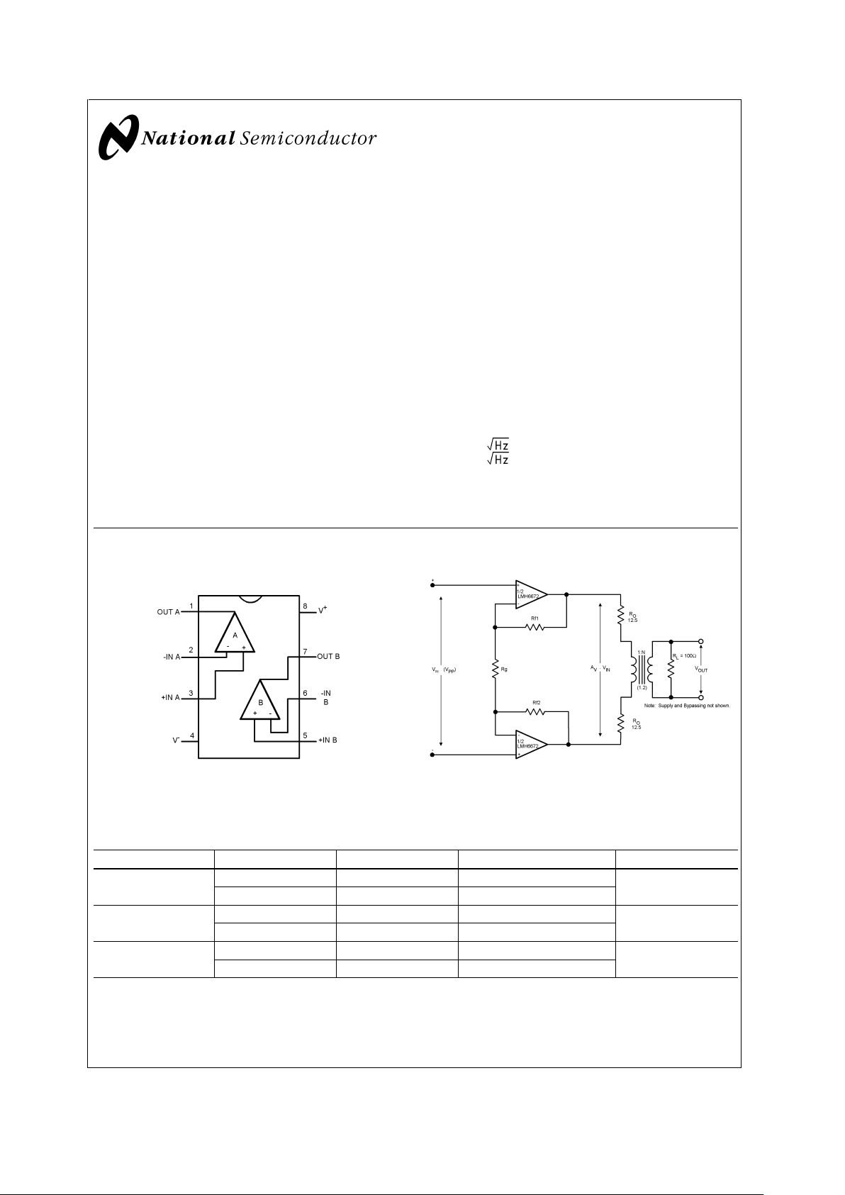
Connection Diagram
8-Pin SOIC/PSOP/LLP
20016602
Top View
Typical Application
20016601
Figure 1
Ordering Information
Package Part Number Package Marking Transport Media NSC Drawing
8-Pin SOIC LMH6672MA LMH6672MA Rails M08A
LMH6672MAX LMH6672MA 2.5k Units Tape and Reel
8-Pin PSOP LMH6672MR LMH6672MR Rails MRA08A
LMH6672MRX LMH6672MR 2.5k Units Tape and Reel
8-Pin LLP LMH6672LD L6672LD 1k Units Tape and Reel LDC08A
LMH6672LDX L6672LD 4.5k Units Tape and Reel
January 2002
LMH6672 Dual, High Output Current, High Speed Op Amp
© 2002 National Semiconductor Corporation DS200166 www.national.com
Page 2
Absolute Maximum Ratings (Note 1)
If Military/Aerospace specified devices are required,
please contact the National Semiconductor Sales Office/
Distributors for availability and specifications.
ESD Tolerance (Note 2)
Human Body Model 2kV
Machine Model 200V
V
IN
Differential
±
1.2V
Output Short Circuit Duration (Note 2)
Supply Voltage (V
+−V−
) 13.2V
Voltage at Input/Output pins V
+
+0.8V, V−−0.8V
Storage Temperature Range −65˚C to +150˚C
Junction Temperature +150˚C (Note 4)
Soldering Information
Infrared or Convection (20 sec) 235˚C
Wave Soldering (10 sec) 260˚C
Operating Ratings (Note 1)
Supply Voltage (V
+-V−
)
±
2.5V to±6.5V
Junction Temperature Range −40˚C to 150˚C
Package Thermal Resistance (θ
JA
)
8-pin SOIC 172˚C/W
8-pin PSOP 58.6˚C/W
8-pin LLP 40˚C/W
Electrical Characteristics
TJ= 25˚C, G = +2, VS=±2.5 to±6V, Rf=RIN= 470Ω,RL= 100Ω; Unless otherwise specified.
Symbol Parameter Conditions Min
(Note 6)
Typ
(Note 5)
Max
(Note 6)
Units
Dynamic Performance
−3dB Bandwidth 130 MHz
0.1dB Bandwidth V
S
=±6V 22 MHz
Slew Rate V
S
=±6V, 4V Step, 10-90% 170 V/µs
Rise and Fall Time V
S
= 6V, 4V Step, 10-90% 18.5 ns
Distortion and Noise Response
2
nd
Harmonic Distortion VO= 8.4VPP, f = 100KHz, RL=25Ω −95 dBc
V
O
= 8.4VPP, f = 1MHz, RL= 100Ω −92 dBc
3
rd
Harmonic Distortion VO= 8.4VPP, f = 100KHz, RL=25Ω −93 dBc
V
O
=2VPP, f = 1MHz, RL= 100Ω −95 dBc
Input Noise Voltage f = 100KHz 4.5 nV
Input Noise Current f = 100KHz 1.7 pA/
Input Characteristics
V
OS
Input Offset Voltage TJ= −40˚C to 150˚C −5.5 −0.2 5.5
mV
−4 −0.2 4
I
B
Input Bias Current TJ= −40˚C to 150˚C 8 14 µA
I
OS
Input Offset Current TJ= −40˚C to 150˚C −2.1 0 2.1 µA
CMVR Common Voltage Range V
S
=±6V −6.0 4.5 V
CMRR Common-Mode Rejection Ratio V
S
=±6V, TJ= −40˚C to 150˚C 150 9.5 µV/V
Transfer Characteristics
A
VOL
Voltage Gain RL= 1k, TJ= −40˚C to 150˚C 1.0 2.5 V/mV
R
L
=25Ω,TJ= −40˚C to 150˚C 0.67 1.7 V/mV
Output Swing R
L
=25Ω,VS=±6V −4.5
±
4.8 4.5
V
R
L
=25Ω,TJ= −40˚C to 150˚C,
V
S
=±6V
−4.4
±
4.8 4.4
Output Swing R
L
= 1k, VS=±6V −4.8
±
4.8 4.8
V
R
L
= 1k, TJ= −40˚C to 150˚C,
V
S
=±6V
−4.7
±
4.8 4.7
I
SC
Output Current (Note 3) VO=0,VS=±6V 400 788 mA
V
O
=0,VS=±6V,
T
J
= −40˚C to 150˚C
260 600 mA
Power Supply
LMH6672
www.national.com 2
Page 3
Electrical Characteristics (Continued)
TJ= 25˚C, G = +2, VS=±2.5 to±6V, Rf=RIN= 470Ω,RL= 100Ω; Unless otherwise specified.
Symbol Parameter Conditions Min
(Note 6)
Typ
(Note 5)
Max
(Note 6)
Units
I
S
Supply Current/Amp VS=±6V 8
mA
V
S
=±6V, TJ= −40˚C to 150˚C 6.2 9
PSRR Power Supply Rejection Ratio V
S
=±2.5V to±6V,
T
J
= −40˚C to 150˚C
72 78 dB
±
2.5V Electrical Characteristics
TJ= 25˚C, G = +2, VS=±2.5 to±6V, Rf=RIN= 470Ω,RL= 100Ω; Unless otherwise specified.
Symbol Parameter Conditions Min
(Note 6)
Typ
(Note 5)
Max
(Note 6)
Units
Dynamic Performance
−3dB Bandwidth 125 MHz
0.1dB Bandwidth 32 MHz
Slew Rate 0.4V Step, 10-90% 115 V/µs
Rise and Fall Time 0.4V Step, 10-90% 2.75 ns
Distortion and Noise Response
2
nd
Harmonic Distortion VO=2VPP, f = 100KHz, RL=25Ω −85 dBc
V
O
=2VPP, f = 1MHz, RL= 100Ω −87 dBc
3
rd
Harmonic Distortion VO=2VPP, f = 100KHz, RL=25Ω −90 dBc
V
O
=2VPP, f = 1MHz, RL= 100Ω −88 dBc
Input Characteristics
V
OS
Input Offset Voltage TJ= −40˚C to 150˚C −5.5 5.5
mV
−4.0 1.1 4.0
I
B
Input Bias Current TJ= −40˚C to 150˚C 8.0 14 µA
CMVR Common-Mode Voltage Range −2.5 1.0 V
CMRR Common-Mode Rejection Ratio T
J
= −40˚C to 150˚C 150 57 µV/V
Transfer Characteristics
A
VOL
Voltage Gain RL=25Ω,TJ= −40˚C to 150˚C 0.67 1.54
V/mV
R
L
= 1k, TJ= −40˚C to 150˚C 1.0 2.0
Output Characteristics
V
O
Output Voltage Swing RL=25Ω 1.20 1.45
VR
L
=25Ω,TJ= −40˚C to 150˚C 1.10 1.35
R
L
= 1k 1.30 1.60
R
L
= 1k, TJ= −40˚C to 150˚C 1.25 1.50
Power Supply
I
S
Supply Current/Amp 8.0
mA
T
J
= −40˚C to 150˚C 5.6 9.0
Note 1: Absolute Maximum Ratings indicate limits beyond which damage to the device may occur. Operating Ratings indicate conditions for which the device is
intended to be functional, but specific performance is not guaranteed. For guaranteed specifications and the test conditions, see the Electrical Characteristics.
Note 2: Human body model, 1.5kΩ in series with 100pF. Machine model, 200Ω in series with 100pF.
Note 3: Shorting the output to either supply or ground will exceed the absolute maximum T
J
and can result in failure.
Note 4: The maximum power dissipation is a function of T
J(MAX)
, θJAand TA. The maximum allowable power dissipation at any ambient temperature is PD=
(T
J(MAX)−TA
)/θJA. All numbers apply for packages soldered directly onto a PC board.
Note 5: Typical values represent the most likely parametric norm.
Note 6: All limits are guaranteed by testing, characterization or statistical analysis.
LMH6672
www.national.com3
Page 4
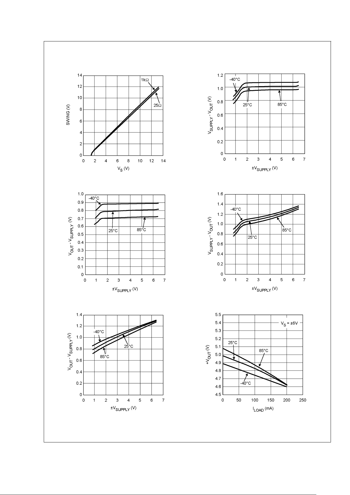
Typical Performance Characteristics At T
J
= 25˚C, RF= 470Ω gain = +2, RL= 100Ω. Unless oth-
erwise specified.
Output Swing R
L
=25Ω,1kΩ@−40˚C, 25˚C, 85˚C Positive Output Swing into 1kΩ
20016635 20016645
Negative Output Swing into 1kΩ Positive Output Swing into 25Ω
20016646
20016644
Negative Output Swing into 25Ω +V
OUT
vs. I
LOAD
20016647 20016640
LMH6672
www.national.com 4
Page 5
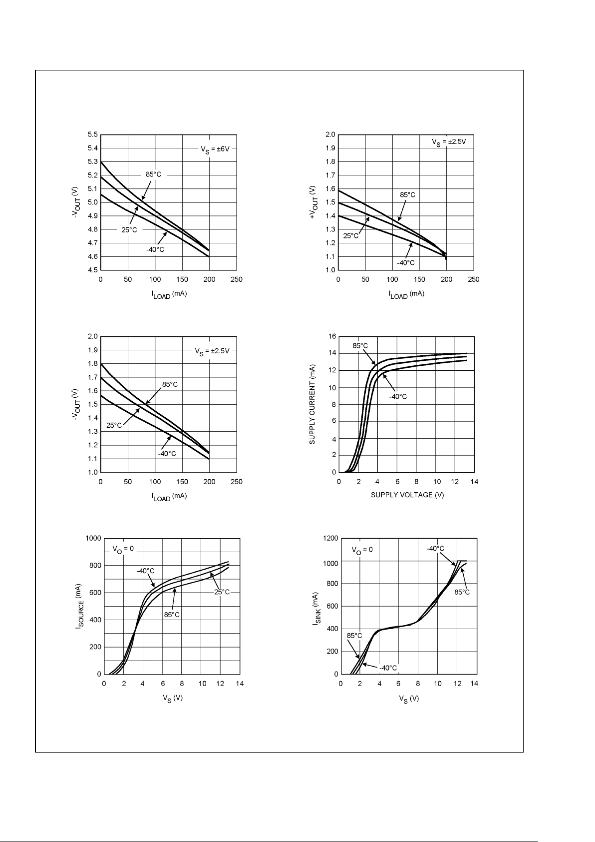
Typical Performance Characteristics At T
J
= 25˚C, RF= 470Ω gain = +2, RL= 100Ω. Unless
otherwise specified. (Continued)
−V
OUT
vs. I
LOAD
+V
OUT
vs. I
LOAD
20016641 20016643
−V
OUT
vs. I
LOAD
Supply Current vs. Supply Voltage
20016642
20016632
Sourcing Current vs. Supply Voltage Sinking Current vs. Supply Voltage
20016633 20016634
LMH6672
www.national.com5
Page 6

Typical Performance Characteristics At T
J
= 25˚C, RF= 470Ω gain = +2, RL= 100Ω. Unless
otherwise specified. (Continued)
V
OS
vs. V
S
VOSvs. VCM,VS= 12V
20016629 20016631
VOSvs. VCM,VS= 5V Bias Current vs. V
SUPPLY
20016630 20016636
Offset Current vs. V
SUPPLY
V
OUT
vs. V
IN
20016637 20016639
LMH6672
www.national.com 6
Page 7

Typical Performance Characteristics At T
J
= 25˚C, RF= 470Ω gain = +2, RL= 100Ω. Unless
otherwise specified. (Continued)
V
OUT
vs. V
IN
Harmonic Distortion vs. Load
20016638
20016620
Harmonic Distortion vs. Load Harmonic Distortion vs. Output Voltage
20016619 20016614
Harmonic Distortion vs. Output Voltage Harmonic Distortion vs. Output Voltage
20016613
20016612
LMH6672
www.national.com7
Page 8

Typical Performance Characteristics At T
J
= 25˚C, RF= 470Ω gain = +2, RL= 100Ω. Unless
otherwise specified. (Continued)
Harmonic Distortion vs. Output Voltage Harmonic Distortion vs. Output Voltage
20016611 20016615
Harmonic Distortion vs. Output Voltage Harmonic Distortion vs. Output Voltage
20016617 20016616
Harmonic Distortion vs. Output Voltage Harmonic Distortion vs. Frequency
20016618 20016622
LMH6672
www.national.com 8
Page 9

Typical Performance Characteristics At T
J
= 25˚C, RF= 470Ω gain = +2, RL= 100Ω. Unless
otherwise specified. (Continued)
Harmonic Distortion vs. Frequency Harmonic Distortion vs. Frequency
20016621 20016623
Harmonic Distortion vs. Frequency Pulse Response, VS=±6V
20016624
20016627
Pulse Response, VS=±2.5V,±6V Pulse Response, (A
VCL
= −1, VS=±6V)
20016628 20016626
LMH6672
www.national.com9
Page 10

Typical Performance Characteristics At T
J
= 25˚C, RF= 470Ω gain = +2, RL= 100Ω. Unless
otherwise specified. (Continued)
Pulse Response, (A
VCL
= −1, VS=±2.5V,±6V) Frequency Response
20016625
20016650
Frequency Response, A
VCL
= +5V Frequency Response, A
VCL
= +10
20016649
20016648
CMRR vs. Frequency@12V CMRR vs. Frequency@5V
20016606 20016605
LMH6672
www.national.com 10
Page 11

Typical Performance Characteristics At T
J
= 25˚C, RF= 470Ω gain = +2, RL= 100Ω. Unless
otherwise specified. (Continued)
PSRR vs. Frequency
@
12V PSRR vs. Frequency@5V
20016608 20016607
en&invs. Frequency@12V en&invs. Frequency@5V
20016610 20016609
LMH6672
www.national.com11
Page 12

Application Notes
Thermal Management
The LMH6672 is a high-speed, high power, dual operational
amplifier with a very high slew rate and very low distortion.
For ease of use, it uses conventional voltage feedback.
These characteristics make the LMH6672 ideal for applications where driving low impedances of 25-100Ω such as
xDSL and active filters.
A class AB output stage allows the LMH6672 to deliver high
currents to low impedance loads with low distortion while
consuming low quiescent supply current. For most op-amps,
class AB topology means that internal power dissipation is
rarely an issue, even with the trend to smaller surface mount
packages. However, the LMH6672 has been designed for
applications where high levels of power dissipation may be
encountered.
Several factors contribute to power dissipation and consequently higher junction temperatures. These factors need to
be well understood if the LMH6672 is to perform to specifications in all applications. This section will examine the
typical application that is shown on the front page of this data
sheet as an example. (Figure 1) Because both amplifiers are
in a single package, the calculations will for the total power
dissipated by both amplifiers.
There are two separate contributors to the internal power
dissipation:
1. The product of the supply voltage and the quiescent
current when no signal is being delivered to the external
load.
2. The additional power dissipated while delivering power
to the external load.
The first of these components appears easy to calculate
simply by inspecting the data sheet. The typical quiescent
supply current for this part is 6.2mA per amplifier, therefore,
with a (6 volt supply, the total power dissipation is:
P
D=VS
x2xlQ= 12 x (12.4x10-3) = 149 mW
(V
S=VCC+VEE
)
With a thermal resistance of 172˚C/W for the SOIC package,
this level of internal power dissipation will result in a junction
temperature (T
J
) of 26˚C above ambient.
Using the worst-case maximum supply current of 18mA and
an ambient of 85˚C, a similar calculation results in a power
dissipation of 216 mW, or a T
J
of 122˚C.
This is approaching the maximum allowed T
J
of 150˚C before a signal is applied. Fortunately,in normal operation, this
term is reduced, for reasons that will soon be explained.
The second contributor to high T
J
is the power dissipated
internally when power is delivered to the external load. This
cause of temperature rise is more difficult to calculate, even
when the actual operating conditions are known.
To maintain low distortion, in a ClassABoutputstage,an idle
current, I
Q
, is maintained through the output transistors
when there is little or no output signal. In the LMH6672,
about 4.8 mAofthetotalquiescentsupplycurrentof12.4mA
flows through the output stages.
Under normal large signal conditions, as the output voltage
swings positive, one transistor of the output pair will conduct
the load current, while the other transistor shuts off, and
dissipates no power. During the negative signal swing this
situation is reversed, with the lower transistor sinking the
load current while the upper transistor is cut off. The current
in each transistor will approximate a half wave rectified
version of the total load current.
Because the output stage idle current is now routed into the
load, 4.8mA can be subtracted from the quiescent supply
current when calculating the quiescent power when the output is driving a load.
The power dissipation caused by driving a load in a DSL
application, using a 1:2 turns ratio transformer driving 20
mW into the subscriber line and 20mW into the back termination resistors, can be calculated as follows:
P
DRIVER
=P
TOT
–(P
TERM+PLINE
) where
P
DRIVER
is the LMH6672 power dissipation
P
TOT
is the total power drawn from the power supply
P
TERM
is the power dissipated in the back termination resis-
tors
P
LINE
is the power sent into the subscriber line
At full specified power, P
TERM=PLINE
= 20mW, P
TOT=VS
xIS.
In this application, V
S
= 12V.
I
S=IQ+AVG|IOUT
|.
I
Q
= the LMH6672 quiescent current minus the output stage
idle current.
I
Q
= 12.4 - 4.8 = 7.6mA
A
VG|IOUT
| for a full-rate ADSL CPE application, using a 1:2
turns ratio transformer, is
= 28.28mA RMS.
For a Gaussian signal, which the DMT ADSL signal approximates, A
VG|IOUT
|= = 22.6mA. Therefore, P
TOT
= (22.6mA + 7.6mA) x 12V = 362mW and P
DRIVER
is 362-40
= 322mW.
In the SOIC package, with a θ
JA
of 172˚C/W, this causes a
temperature rise of 55˚C. With an ambient temperature at
the maximum recommended 85˚C, the T
J
is at 140˚C, well
below the specified 150˚C maximum.
Even if we assume the absolute maximum I
S
over tempera-
ture of 18mA, when we scale up the I
Q
proportionally to 7mA,
the P
DRIVER
only goes up by 41mW causing a 62˚C rise to
147˚C.
Although very few CPE applications will ever operate in an
environment as hot as 85˚C, if a lower T
J
is desired or the
LMH6672 is to be used in an application where the power
dissipation is higher, the PSOP package provides a much
lower θ
JA
of only 58.6˚C/W.
Using the same P
DRIVER
as above, we find that the tempera-
ture rise is only 19˚ and 21˚C, resulting in T
J
’s in an 85˚C
ambient of 104˚C and 106˚C respectively.
Circuit Layout Considerations
National Semiconductor suggests the following evaluation
boards as a guide for high frequency layout and as an aid in
device testing and characterization. Since the exposed PAD
(or DAP) of the PSOP and LLP package is internally floating,
the footprint for DAP could be connected to ground plane in
PCB for better heat dissipation.
Device Package Evaluation
Board PN
LMH6672MA 8-Pin SOIC CLC730036
LMH6672LD 8-Pin LLP CLC730114
LMH6672MR 8-Pin PSOP CLC730121
These free evaluation boards are shipped when a device
sample request is placed with National Semiconductor.
LMH6672
www.national.com 12
Page 13

Physical Dimensions inches (millimeters)
unless otherwise noted
8-Pin SOIC
NS Package Number M08A
8-Pin PSOP
NS Package Number MRA08A
LMH6672
www.national.com13
Page 14

Physical Dimensions inches (millimeters) unless otherwise noted (Continued)
8-Pin LLP
NS Package Number LDC08A
LIFE SUPPORT POLICY
NATIONAL’S PRODUCTS ARE NOT AUTHORIZED FOR USE AS CRITICAL COMPONENTS IN LIFE SUPPORT
DEVICES OR SYSTEMS WITHOUT THE EXPRESS WRITTEN APPROVAL OF THE PRESIDENT AND GENERAL
COUNSEL OF NATIONAL SEMICONDUCTOR CORPORATION. As used herein:
1. Life support devices or systems are devices or
systems which, (a) are intended for surgical implant
into the body, or (b) support or sustain life, and
whose failure to perform when properly used in
accordance with instructions for use provided in the
labeling, can be reasonably expected to result in a
significant injury to the user.
2. A critical component is any component of a life
support device or system whose failure to perform
can be reasonably expected to cause the failure of
the life support device or system, or to affect its
safety or effectiveness.
National Semiconductor
Corporation
Americas
Email: support@nsc.com
National Semiconductor
Europe
Fax: +49 (0) 180-530 85 86
Email: europe.support@nsc.com
Deutsch Tel: +49 (0) 69 9508 6208
English Tel: +44 (0) 870 24 0 2171
Français Tel: +33 (0) 1 41 91 8790
National Semiconductor
Asia Pacific Customer
Response Group
Tel: 65-2544466
Fax: 65-2504466
Email: ap.support@nsc.com
National Semiconductor
Japan Ltd.
Tel: 81-3-5639-7560
Fax: 81-3-5639-7507
www.national.com
LMH6672 Dual, High Output Current, High Speed Op Amp
National does not assume any responsibility for use of any circuitry described, no circuit patent licenses are implied and National reserves the right at any time without notice to change said circuitry and specifications.
 Loading...