

Page 1
LMH6654/55
Single/Dual Low Power, 250 MHz, Low Noise Amplifiers
General Description
The LMH6654/55 single and dual high speed, voltage feedback amplifiers are designed to have unity-gain stable operation with a bandwidth of 250MHz. They operate from
±
2.5V to±6V and each channel consumes only 4.5mA. The
amplifiers feature very low voltage noise and wide output
swing to maximize signal-to-noise ratio.
The LMH6654/55 have a true single supply capability with
input common mode voltage range extending 150 mV below
negative rail and within 1.3V of the positive rail.
LMH6654/55 high speed and low power combination make
these products an ideal choice for many portable, high
speed application where power is at a premium.
The LMH6654 is packaged in SOT23-5 and SOIC-8. The
LMH6655 is packaged in MSOP-8 and SOIC-8.
The LMH6654/55 are built on National’s Advance VIP10
™
(Vertically Integrated PNP) complementary bipolar process.
Features
(VS=±5V, TJ= 25˚C, Typical values unless specified).
n Voltage feedback architecture
n Unity gain bandwidth 250MHz
n Supply voltage range
±
2.5V to±6V
n Slew rate 200V/µsec
n Supply current 4.5mA/channel
n Input common mode voltage −5.15V to +3.7V
n Output voltage swing (R
L
= 100Ω) −3.6V to 3.4V
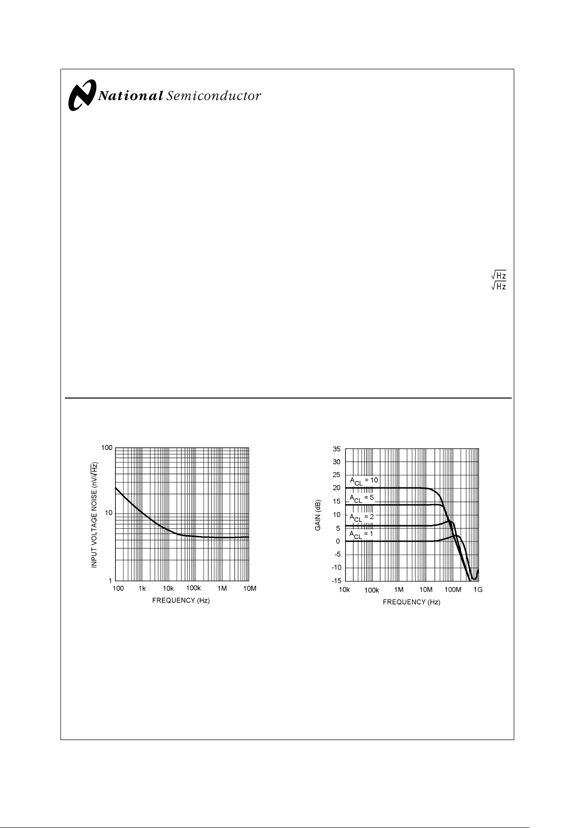
n Input voltage noise 4.5nV/
n Input current noise 1.7pA/
n Settling Time to 0.01% 25ns
Applications
n ADC drivers
n Consumer video
n Active filters
n Pulse delay circuits
n xDSL receiver
n Pre-amps
Typical Performance Characteristics
Input Voltage Noise vs. Frequency Closed Loop Gain vs. Frequency
20016560 20016558
August 2001
LMH6654/55 Single/Dual Low Power, 250 MHz, Low Noise Amplifiers
© 2001 National Semiconductor Corporation DS200165 www.national.com
Page 2
Absolute Maximum Ratings (Note 1)
If Military/Aerospace specified devices are required,
please contact the National Semiconductor Sales Office/
Distributors for availability and specifications.
ESD Tolerance (Note 2)
Human Body Model 2kV
Machine Model 200V
V
IN
Differential
±
1.2V
Output Short Circuit Duration (Note 3)
Supply Voltage (V
+−V−
) 13.2V
Voltage at Input pins V
+
+0.5V, V−−0.5V
Storage Temperature Range −65˚C to +150˚C
Junction Temperature (Note 4) +150˚C
Soldering Information
Infrared or Convection (20 sec.) 235˚C
Wave Soldering (10 sec.) 260˚C
Operating Ratings (Note 1)
Supply Voltage (V
+-V−
)
±
2.5V to±6.0V
Junction Temperature Range −40˚C to +85˚C
Thermal Resistance (θ
JA
)
8-Pin SOIC 172˚C/W
8-Pin MSOP 235˚C/W
5-Pin SOT-23 265˚C/W
±
5V Electrical Characteristics
Unless otherwise specified, all limits guaranteed for TJ= 25˚C, V+= +5V, V−= −5V, VCM= 0V, AV= +1, RF=25Ωfor gain =
+1, R
F
= 402Ω for gain = ≥ +2, and RL= 100Ω. Boldface limits apply at the temperature extremes.
Symbol Parameter Conditions Min
(Note 6)
Typ
(Note 5)
Max
(Note 6)
Units
Dynamic Performance
f
CL
Close Loop Bandwidth AV= +1 250
MHz
A
V
= +2 130
A
V
=+5 52
A
V
= +10 26
GBWP Gain Bandwidth Product A
V
≥ +5 260 MHz
Bandwidth for 0.1dB Flatness A
V
+1 18 MHz
φm Phase Margin 50 deg
SR Slew Rate (Note 8) A
V
= +1, VIN=2V
PP
200 V/µs
T
S
Settling Time
0.01%
AV= +1, 2V Step 25 ns
0.1% 15 ns
t
r
Rise Time AV= +1, 0.2V Step 1.4 ns
t
f
Fall Time AV= +1, 0.2V Step 1.2 ns
Distortion and Noise Response
e
n
Input Referred Voltage Noise f ≥ 0.1 MHz 4.5 nV/
i
n
Input-Referred Current Noise f ≥ 0.1 MHz 1.7 pA/
Second Harmonic Distortion AV= +1, f = 5MHz −80
dBc
Third Harmonic Distortion V
O
=2VPP,RL= 100Ω −85
X
t
Crosstalk (for LMH6655 only) Input Referred, 5MHz,
Channel-to-Channel
−80 dB
DG Differential Gain A
V
= +2, NTSC, RL= 150Ω 0.01 %
DP Differential Phase A
V
= +2, NTSC, RL= 150Ω 0.025 deg
Input Characteristics
V
OS
Input Offset Voltage VCM=0V −3
−4
±
13
4
mV
TC V
OS
Input Offset Average Drift VCM= 0V (Note 7) 6 µV/˚C
I
B
Input Bias Current VCM=0V 5 12
18
µA
I
OS
Input Offset Current VCM=0V −1
−2
0.3 1
2
µA
R
IN
Input Resistance Common- Mode 4 MΩ
Differential Mode 20 kΩ
LMH6654/55
www.national.com 2
Page 3
±
5V Electrical Characteristics (Continued)
Unless otherwise specified, all limits guaranteed for TJ= 25˚C, V+= +5V, V−= −5V, VCM= 0V, AV= +1, RF=25Ωfor gain =
+1, R
F
= 402Ω for gain = ≥ +2, and RL= 100Ω. Boldface limits apply at the temperature extremes.
Symbol Parameter Conditions Min
(Note 6)
Typ
(Note 5)
Max
(Note 6)
Units
C
IN
Input Capacitance Common- Mode 1.8 pF
Differential Mode 1
CMRR Common Mode Rejection Ration Input Referred,
V
CM
=0Vto−5V
70
68
90 dB
CMVR Input Common- Mode Voltage Range CMRR ≥ 50dB −5.15 −5.0
V
3.5 3.7
Transfer Characteristics
A
VOL
Large Signal Voltage Gain VO=4VPP,RL= 100Ω 60
58
67 dB
Output Characteristics
V
O
Output Swing High No Load 3.4
3.2
3.6
V
Output Swing Low No Load −3.9 −3.7
−3.5
Output Swing High R
L
= 100Ω 3.2
3.0
3.4
Output Swing Low R
L
= 100Ω −3.6 −3.4
−3.2
I
SC
Short Circuit Current (Note 3) Sourcing, VO=0V
∆V
IN
= 200mV
145
130
280
mA
Sinking, V
O
=0V
∆V
IN
= 200mV
100
80
185
I
OUT
Output Current Sourcing, VO= +3V 80
mA
Sinking, V
O
= −3V 120
R
O
Output Resistance AV= +1, f<100kHz 0.08 Ω
Power Supply
PSRR Power Supply Rejection Ratio Input Referred ,
V
S
=±5V to±6V
60 76 dB
I
S
Supply Current (per channel) 4.5 6
7
mA
5V Electrical Characteristics
Unless otherwise specified, all limits guaranteed for TJ= 25˚C, V+= +5V, V−= −0V, VCM= 2.5V, AV= +1, RF=25Ωfor gain
= +1, R
F
= 402Ω for gain = ≥ +2, and RL= 100Ω to V+/2. Boldface limits apply at the temperature extremes.
Symbol Parameter Conditions Min
(Note 6)
Typ
(Note 5)
Max
(Note 6)
Units
Dynamic Performance
f
CL
Close Loop Bandwidth AV= +1 230
MHz
A
V
= +2 120
A
V
=+5 50
A
V
= +10 25
GBWP Gain Bandwidth Product A
V
≥ +5 250 MHz
Bandwidth for 0.1dB Flatness A
V
= +1 17 MHz
φm Phase Margin 48 deg
SR Slew Rate (Note 8) A
V
= +1, VIN=2V
PP
190 V/µs
T
S
Settling Time
0.01%
AV= +1, 2V Step 30 ns
0.1% 20 ns
LMH6654/55
www.national.com3
Page 4
5V Electrical Characteristics (Continued)
Unless otherwise specified, all limits guaranteed for TJ= 25˚C, V+= +5V, V−= −0V, VCM= 2.5V, AV= +1, RF=25Ωfor gain
= +1, R
F
= 402Ω for gain = ≥ +2, and RL= 100Ω to V+/2. Boldface limits apply at the temperature extremes.
Symbol Parameter Conditions Min
(Note 6)
Typ
(Note 5)
Max
(Note 6)
Units
t
r
Rise Time AV= +1, 0.2V Step 1.5 ns
t
f
Fall Time AV= +1, 0.2V Step 1.35 ns
Distortion and Noise Response
e
n
Input Referred Voltage Noise f ≥ 0.1MHz 4.5 nV/
i
n
Input Referred Current Noise f ≥ 0.1 MHz 1.7 pA/
Second Harmonic Distortion AV= +1, f = 5MHz −65
dBc
Third Harmonic Distortion V
O
=2VPP,RL= 100Ω −70
X
t
Crosstalk (for LMH6655 only) Input Referred, 5MHz −78 dB
Input Characteristics
V
OS
Input Offset Voltage VCM= 2.5V −5
−6.5
±
25
6.5
mV
TC V
OS
Input Offset Average Drift VCM= 2.5V (Note 7) 6 µV/˚C
I
B
Input Bias Current VCM= 2.5V 6 12
18
µA
I
OS
Input Offset Current VCM= 2.5V −2
−3
0.5 2
3
µA
R
IN
Input Resistance Common- Mode 4 MΩ
Differential Mode 20 kΩ
C
IN
Input Capacitance Common- Mode 1.8 pF
Differential Mode 1
CMRR Common Mode Rejection Ration Input Referred,
V
CM
= 0V to −2.5V
70
68
90 dB
CMVR Input Common Mode Voltage Range CMRR ≥ 50dB −0.15 0
V
3.5 3.7
Transfer Characteristics
A
VOL
Large Signal Voltage Gain VO= 1.6VPP,RL= 100Ω 58
55
64 dB
Output Characteristics
V
O
Output Swing High No Load 3.6
3.4
3.75
V
Output Swing Low No Load 0.9 1.1
1.3
Output Swing High R
L
= 100Ω 3.5
3.35
3.70
Output Swing Low R
L
= 100Ω 1 1.3
1.45
I
SC
Short Circuit Current (Note 3) Sourcing , VO= 2.5V
∆V
IN
= 200mV
90
80
170
mA
Sinking, V
O
= 2.5V
∆V
IN
= 200mV
70
60
140
I
OUT
Output Current Sourcing, VO= +3.5V 30
mA
Sinking, V
O
= 1.5V 60
R
O
Output Resistance AV= +1, f<100kHz .08 Ω
Power Supply
PSRR Power Supply Rejection Ratio Input Referred ,
V
S
=±2.5V to±3V
60 75 dB
I
S
Supply Current (per channel) 4.5 6
7
mA
LMH6654/55
www.national.com 4
Page 5
5V Electrical Characteristics (Continued)
Note 1: Absolute Maximum Ratings indicate limits beyond which damage to the device may occur. Operating Ratings indicate conditions for which the device is
intended to be functional, but specificperformanceisnotguaranteed.For guaranteed specifications and the test conditions, see the Electrical Characteristics Table.
Note 2: Human body model, 1.5kΩ in series with 100pF. Machine model: 0Ω in series with 100pF.
Note 3: Continuous short circuit operation at elevated ambient temperature can result in exceeding the maximum allowed junction temperature at 150˚C.
Note 4: The maximum power dissipation is a function of T
J(MAX)
, θJAand TA. The maximum allowable power dissipation at any ambient temperature is PD=
(T
J(MAX)−TA
)/θJA. All numbers apply for packages soldered directly onto a PC board.
Note 5: Typical Values represent the most likely parametric norm.
Note 6: All limits are guaranteed by testing or statistical analysis.
Note 7: Offset voltage average drift is determined by dividing the change in V
OS
at temperature extremes into the total temperature change.
Note 8: Slew rate is the slower of the rising and falling slew rates. Slew rate is rate of change from 10% to 90% of output voltage step.
Typical Performance Characteristics T
J
= 25˚C, V+=±5V, V−= −5, RF=25Ωfor gain = +1, RF=
402Ω and for gain ≥ +2, and R
L
= 100Ω, unless otherwise specified.
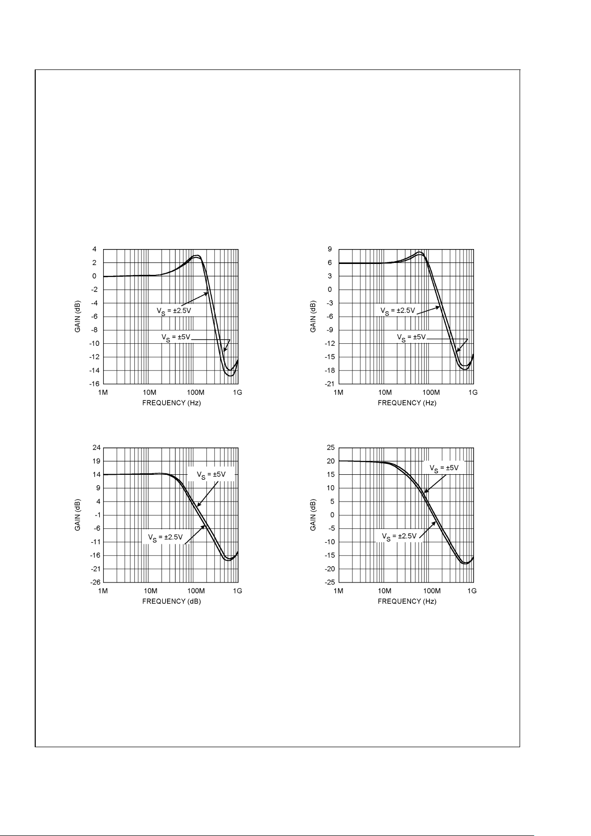
Closed Loop Bandwidth (G = +1) Closed Loop Bandwidth (G = +2)
20016509 20016510
Closed Loop Bandwidth (G = +5) Closed Loop Bandwidth (G = +10)
20016511 20016512
LMH6654/55
www.national.com5
Page 6
Typical Performance Characteristics T
J
= 25˚C, V+=±5V, V−= −5, RF=25Ωfor gain = +1, RF=
402Ω and for gain ≥ +2, and R
L
= 100Ω, unless otherwise specified. (Continued)
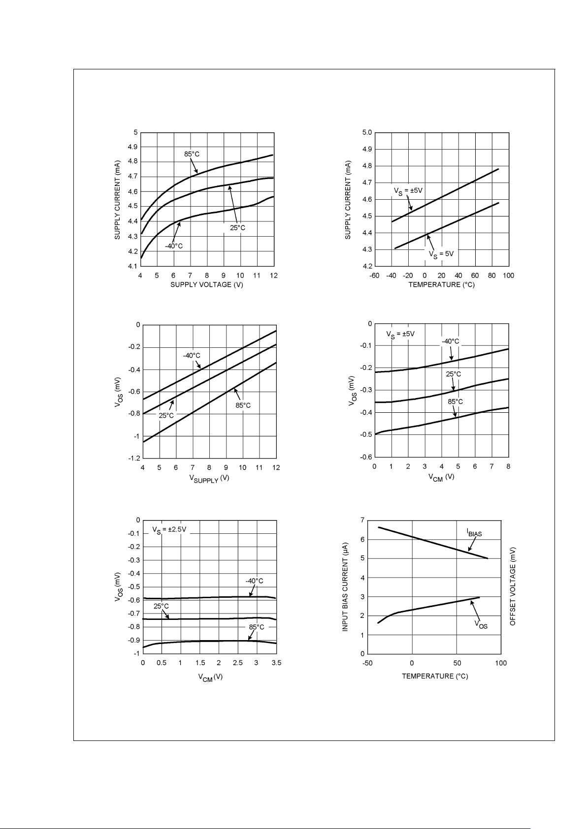
Supply Current per Channel vs. Supply Voltage Supply Current per Channel vs. Temperature
20016535 20016548
Offset Voltage vs. Supply Voltage (VCM= 0V) Offset Voltage vs. Common Mode
20016549
20016532
Offset Voltage vs. Common Mode Bias Current and Offset Voltage vs. Temperature
20016539
20016551
LMH6654/55
www.national.com 6
Page 7

Typical Performance Characteristics T
J
= 25˚C, V+=±5V, V−= −5, RF=25Ωfor gain = +1, RF=
402Ω and for gain ≥ +2, and R
L
= 100Ω, unless otherwise specified. (Continued)
Bias Current vs. Common Mode Voltage A
OL
, PSRR and CMRR vs. Temperature
20016537
20016550
Inverting Large Signal Pulse Response (VS= 5V) Inverting Large Signal Pulse Response (VS=±5V)
20016502 20016504
Non-Inverting Large Signal Pulse Response (VS= 5V) Non-Inverting Large Signal Pulse Response (VS=±5V)
20016506 20016508
LMH6654/55
www.national.com7
Page 8

Typical Performance Characteristics T
J
= 25˚C, V+=±5V, V−= −5, RF=25Ωfor gain = +1, RF=
402Ω and for gain ≥ +2, and R
L
= 100Ω, unless otherwise specified. (Continued)
Non-Inverting Small Signal Pulse Response (V
S
= 5V) Non-Inverting Small Signal Pulse Response (VS=±5V)
20016505 20016507
Inverting Small Signal Pulse Response (VS= 5V) Inverting Small Signal Pulse Response (VS=±5V)
20016501 20016503
Input Voltage and Current Noise vs. Frequency (VS= 5V)
Input Voltage and Current Noise vs. Frequency
(VS=±5V)
20016513 20016514
LMH6654/55
www.national.com 8
Page 9

Typical Performance Characteristics T
J
= 25˚C, V+=±5V, V−= −5, RF=25Ωfor gain = +1, RF=
402Ω and for gain ≥ +2, and R
L
= 100Ω, unless otherwise specified. (Continued)
Harmonic Distortion vs. Frequency
G = +1, V
O
=2VPP,VS=5V
Harmonic Distortion vs. Frequency
G = +1, VO=2VPP,VS=±5V
20016517 20016518
Harmonic Distortion vs. Temperature
V
S
= 5V, f = 5MHz, VO=2V
PP
Harmonic Distortion vs. Temperature
V
S
=±5V, f = 5MHz, VO=2V
PP
20016529 20016528
Harmonic Distortion vs. Gain
V
S
= 5V, f = 5MHz, VO=2V
PP
Harmonic Distortion vs. Gain
V
S
=±5V, f = 5MHz, VO=2V
PP
20016531 20016530
LMH6654/55
www.national.com9
Page 10

Typical Performance Characteristics T
J
= 25˚C, V+=±5V, V−= −5, RF=25Ωfor gain = +1, RF=
402Ω and for gain ≥ +2, and R
L
= 100Ω, unless otherwise specified. (Continued)
Harmonic Distortion vs. Output Swing
(G = +2, V
S
= 5V, f = 5MHz)
Harmonic Distortion vs. Output Swing
(G = +2, VS=±5V, f = 5MHz)
20016559
20016522
PSRR vs. Frequency CMRR vs. Frequency
20016516
20016564
Output Sinking Current Output Sourcing Current
20016546 20016547
LMH6654/55
www.national.com 10
Page 11

Typical Performance Characteristics T
J
= 25˚C, V+=±5V, V−= −5, RF=25Ωfor gain = +1, RF=
402Ω and for gain ≥ +2, and R
L
= 100Ω, unless otherwise specified. (Continued)
CrossTalk vs. Frequency (LMH6655 only) CrossTalk vs. Frequency (LMH6655 only)
20016561 20016562
Isolation Resistance vs. Capacitive Load Open Loop Gain and Phase vs. Frequency
20016563
20016527
LMH6654/55
www.national.com11
Page 12

Connection Diagrams
LMH6654 in SOIC LMH6654 in SOT23-5 LMH6655 in SOIC and MSOP
20016521
Top View
20016520
Top View
20016519
Top View
Ordering Information
Package Part Number Package Marking Transport Media NSC Drawing
8-Pin SOIC LMH6654MA LMH6654MA 95 Units Rails M08A
LMH6654MAX 2.5k Units Tape and Reel
LMH6655MA LMH6655MA 95 Units Rails
LMH6655MAX 2.5k Units Tape and Reel
5-Pin SOT23-5 LMH6654MF A66A 1k Units Tape and Reel MF05A
LMH6654MFX 3K Units Tape and Reel
8-Pin MSOP LMH6655MM A67A 1k Units Tape and Reel MUA08A
LMH6655MMX 3.5k Units Tape and Reel
Application Information
General Information
The LMH6654 single and LMH6655 dual high speed, voltage
feedback amplifiers are manufactured on National Semiconductor’s new VIP10 (Vertically Integrated PNP) complementary bipolar process. These amplifiers can operate from
±
2.5V to±6V power supply. They offer low supply current,
wide bandwidth, very low voltage noise and large output
swing. Many of the typical performance plots found in the
datasheet can be reproduced if 50Ω coax and 50Ω R
IN/ROUT
resistors are used.
Circuit Layout Consideration
With all high frequency devices, board layouts with stray
capacitance have a strong influence on theAC performance.
The LMH6654/55 are not exception and the inverting input
and output pins are particularly sensitive to the coupling of
parasitic capacitance to AC ground. Parasitic capacitances
on the inverting input and output nodes to ground could
cause frequency response peaking and possible circuit oscillation. Therefore, the power supply, ground traces and
ground plan should be placed away from the inverting input
and output pins. Also, it is very important to keep the parasitic capacitance across the feedback to an absolute minimum.
The PCB should have a ground plane covering all unused
portion of the component side of the board to provide a low
impedance path. All trace lengths should be minimized to
reduce series inductance.
Supply bypassing is required for the amplifiers performance.
The bypass capacitors provide a low impedance return current path at the supply pins. They also provide high frequency filtering on the power supply traces. It is recommended that a ceramic decoupling capacitor 0.1µF chip
should be placed with one end connected to the ground
plane and the other side as close as possible to the power
pins. An additional 10µF tantalum electrolytic capacitor
should be connected in parallel, to supply current for fast
large signal changes at the output.
Evaluation Boards
National provides the following evaluation boards as a guide
for high frequency layout and as an aid in device testing and
characterization.
Device Package Evalulation
Board PN
LMH6654MF SOT23-5 CLC730068
LMH6654MA 8-Pin SOIC CLC730027
LMH6655MA 8-Pin SOIC CLC730036
LMH6655MM 8-Pin MSOP CLC730123
20016541
FIGURE 1.
LMH6654/55
www.national.com 12
Page 13

Application Information (Continued)
The free evaluation board are shipped automatically when a
device sample request is placed with National Semiconductor.
The CLC730027 datasheet also contains tables of recommended components to evaluate several of National’s high
speed amplifiers. This table for the LMH6654 is illustrated
below. Refer to the evaluation board datasheet for schematics and further information.
Components Needed to Evaluate the LMH6654 on the
Evaluation Board:
•
RfRguse the datasheet to select values.
•
RIN,R
OUT
typically 50Ω (Refer to the Basic Operation
section of the evaluation board datasheet for details)
•
Rfis an optional resistor for inverting again configurations
(select R
f
to yield desired input impedance = Rg||Rf)
•
C1,C2use 0.1µF ceramic capacitors
•
C3,C4use 10µF tantalum capacitors
Components not used:
1. C
5,C6,C7,C8
2. R1 thru R8
The evaluation boards are designed to accommodate dual
supplies. The board can be modified to provide single operation. For best performance;
1) do not connect the unused supply.
2) ground the unused supply pin.
power Dissipation
The package power dissipation should be taken into account
when operating at high ambient temperature and/or high
power dissipative conditions. In determining maximum operable temperature of the device, make sure the total power
dissipation of the device is considered; this power dissipated
in the device with a load connected to the output as well as
the nominal dissipation of the op amp.
Driving Capacitive Loads
Capacitive loads decrease the phase margin of all op amps.
The output impedance of a feedback amplifier becomes
inductive at high frequencies, creating a resonant circuit
when the load is capacitive. This can lead to overshoot,
ringing and oscillation. To eliminate oscillation or reduce
ringing, an isolation resistor can be placed as shown in
Figure 2
below. At frequencies above
the load impedance of the Amplifier approaches R
ISO
. The
desired performance depends on the value of the isolation
resistor. The isolation resistance vs. capacitance load graph
in the typical performance characteristics provides the
means for selection of the value of R
S
that provides ≤ 3dB
peaking in closed loop A
V
= 1 response. In general, the
bigger the isolation resistor, the more damped the pulse
response becomes. For initial evaluation, a 50Ω isolation
resistor is recommended.
Components Selection and Feedback Resistor
It is important in high-speed applications to keep all component leads short since wires are inductive at high frequency.
For discrete components, choose carbon composition axially
leaded resistors and micro type capacitors. Surface mount
components are preferred over discrete components for
minimum inductive effect. Never use wire wound type resistors in high frequency applications.
Large values of feedback resistors can couple with parasitic
capacitance and cause undesired effects such as ringing or
oscillation in high-speed amplifiers. Keep resistors as low as
possible consistent with output loading consideration. For a
gain of 2 and higher, 402Ω feedback resistor used for the
typical performance plots gives optimal performance. For
unity gain follower, a 25Ω feedback resistor is recommended
rather than a direct short. This effectively reduces the Q of
what would otherwise be a parasitic inductance (the feedback wire) into the parasitic capacitance at the inverting
input.
Bias Current Cancellation
In order to cancel the bias current errors of the non-inverting
configuration, the parallel combination of the gain setting R
g
and feedback Rfresistors should equal the equivalent
source resistance R
seq
as defined in
Figure 3
. Combining
this constraint with the non-inverting gain equation, allows
both R
f
and Rgto be determined explicitly from the following
equations:
R
f=AVRseq
and Rg=Rf/(AV−1)
For inverting configuration, bias current cancellation is accomplished by placing a resistor R
b
on the non-inverting
input equal in value to the resistance seen by the inverting
input (R
f
//(Rg+Rs). The additional noise contribution of R
b
can be minimized through the use of a shunt capacitor.
20016540
FIGURE 2.
LMH6654/55
www.national.com13
Page 14

Application Information (Continued)
Total Input Noise vs. Source Resistance
The noise model for the non-inverting amplifier configuration
showing all noise sources is described in
Figure 5
. In addi-
tion to the intrinsic input voltage noise (e
n
) and current noise
(i
n=in+=in−
) sources, there also exits thermal voltage noise
associated with each of the external resistors.
Equation 1 provides the general form for total equivalent
input voltage noise density (e
ni
). Equation 2 is a simplifica-
tion of Equation 1 that assumes
(1)
R
f
||Rg=R
seq
for bias current cancellation.
Figure 6
illustrates
the equivalent noise model using this assumption. The total
equivalent output voltage noise (e
no
)ise
ni
*
AV.
(2)
If bias current cancellation is not a requirement, then R
f
||R
g
does not need to equal R
seq
. In this case, according to
Equation 1, R
fRg
should be as low as possible in order to
minimize noise. Results similar to Equation 1 are obtained
for the inverting configuration on
Figure 2
if R
seq
is replaced
by R
b
and Rgis replaced by Rg+Rs. With these substitu-
tions, Equation 1 will yield an e
ni
referred to the non-inverting
input. Referring to e
ni
to the inverting input is easily accom-
plished by multiplying e
ni
by the ration of non-inverting to
inverting gains.
Noise Figure
Noise Figure (NF) is a measure of the noise degradation
caused by an amplifier.
(3)
The noise figure formula is shown is Equation 3. The addition of a terminating resistor R
T
, reduces the external ther-
mal noise but increases the resulting NF.
20016542
FIGURE 3. Non-Inverting Amplifier Configuration
20016543
FIGURE 4. Inverting Amplifier Configuration
20016544
FIGURE 5. Non-Inverting Amplifier Noise Model
20016545
FIGURE 6. Noise Model with Rf||Rg=R
seq
LMH6654/55
www.national.com 14
Page 15

Application Information (Continued)
The NF is increased because the R
T
reduces the input signal
amplitude thus reducing the input SNR.
(4)
The noise figure is related to the equivalent source resistance (R
seq
) and the parallel combination of Rfand Rg. To minimize noise
figure, the following steps are recommended:
1. Minimize R
f
||R
g
2. Choose the Optimum Rs(R
OPT
)
R
OPT
is the point at which the NF curve reaches a minimum and is approximated by:
R
OPT
≈ (en/in)
LMH6654/55
www.national.com15
Page 16

Physical Dimensions inches (millimeters) unless otherwise noted
8-Pin SOIC
NS Package Number M08A
5-Pin SOT23
NS Package Number MF05A
LMH6654/55
www.national.com 16
Page 17

Physical Dimensions inches (millimeters) unless otherwise noted (Continued)
8-Pin MSOP
NS Package Number MUA08A
LIFE SUPPORT POLICY
NATIONAL’S PRODUCTS ARE NOT AUTHORIZED FOR USE AS CRITICAL COMPONENTS IN LIFE SUPPORT
DEVICES OR SYSTEMS WITHOUT THE EXPRESS WRITTEN APPROVAL OF THE PRESIDENT AND GENERAL
COUNSEL OF NATIONAL SEMICONDUCTOR CORPORATION. As used herein:
1. Life support devices or systems are devices or
systems which, (a) are intended for surgical implant
into the body, or (b) support or sustain life, and
whose failure to perform when properly used in
accordance with instructions for use provided in the
labeling, can be reasonably expected to result in a
significant injury to the user.
2. A critical component is any component of a life
support device or system whose failure to perform
can be reasonably expected to cause the failure of
the life support device or system, or to affect its
safety or effectiveness.
National Semiconductor
Corporation
Americas
Email: support@nsc.com
National Semiconductor
Europe
Fax: +49 (0) 180-530 85 86
Email: europe.support@nsc.com
Deutsch Tel: +49 (0) 69 9508 6208
English Tel: +44 (0) 870 24 0 2171
Français Tel: +33 (0) 1 41 91 8790
National Semiconductor
Asia Pacific Customer
Response Group
Tel: 65-2544466
Fax: 65-2504466
Email: ap.support@nsc.com
National Semiconductor
Japan Ltd.
Tel: 81-3-5639-7560
Fax: 81-3-5639-7507
www.national.com
LMH6654/55 Single/Dual Low Power, 250 MHz, Low Noise Amplifiers
National does not assume any responsibility for use of any circuitry described, no circuit patent licenses are implied and National reserves the right at any time without notice to change said circuitry and specifications.
 Loading...