

Page 1
LMH6645/46/47
2.7V, 650µA, 55MHz, Rail-to-Rail Input and Output
Amplifiers with Shutdown Option
February 2002
LMH6645/46/47 2.7V, 650µA, 55MHz, Rail-to-Rail Input and Output Amplifiers with Shutdown
Option
General Description
The LMH6645 (single) and LMH6646 (dual), rail-to-rail input
and output voltage feedback amplifiers, offer high speed
(55MHz), and low voltage operation (2.7V) in addition to
micro-power shutdown capability (LMH6647, single).
Input common modevoltage range exceeds either supply by
0.3V, enhancing ease of use in multitude of applications
where previously only inferior devices could be used. Output
voltage range extends to within 20mV of either supply rails,
allowing wide dynamic range especially in low voltage applications. Even with low supply current of 650µA/amplifier,
output current capability is kept at a respectable
driving heavier loads. Important device parameters such as
BW, Slew Rate and output current are kept relatively independent of the operating supply voltage by a combination of
process enhancements and design architecture.
In portable applications, the LMH6647 provides shutdown
capability while keeping the turn-off current to less than
50µA. Both turn-on and turn-off characteristics are well behaved with minimal output fluctuations during transitions.
This allows the part to be used in power saving mode, as
well as multiplexing applications. Miniature packages
(SOT23, MSOP-8, and SO-8) are further means to ease the
adoption of these low power high speed devices in applications where board area is at a premium.
±
20mA for
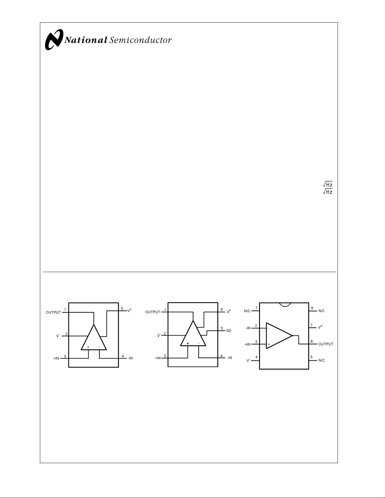
Connection Diagrams
Features
(VS= 2.7V, TA= 25˚C, RL=1kΩto V+/2, AV= +1. Typical
values unless specified).
n −3dB BW 55MHz
n Supply voltage range 2.5V to 12V
n Slew rate 22V/µs
n Supply current 650µA/channel
n Output short circuit current 42mA
n Linear output current
n Input common mode voltage 0.3V beyond rails
n Output voltage swing 20mV from rails
n Input voltage noise 17nV/
n Input current noise 0.75pA/
±
20mA
Applications
n Active filters
n High speed portable devices
n Multiplexing applications (LMH6647)
n Current sense buffer
n High speed transducer amp
SOT23-5 (LMH6645) SOT23-6 (LMH6647) SOIC-8 (LMH6645)
Top View
20020259
© 2002 National Semiconductor Corporation DS200202 www.national.com
Top View
20020260
Top View
20020261
Page 2
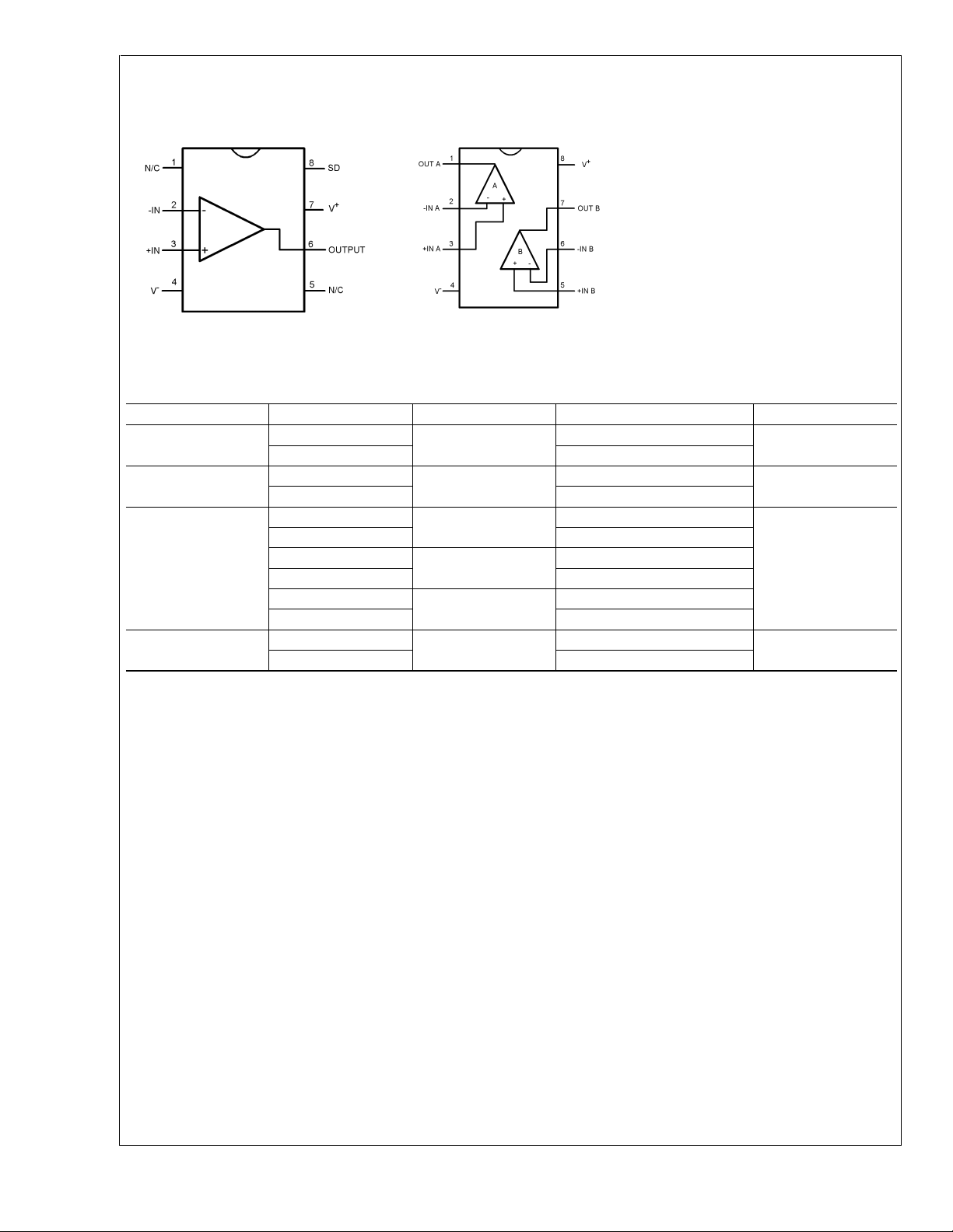
Connection Diagrams (Continued)
SOIC-8 (LMH6647)
LMH6645/46/47
SOIC-8 and MSOP-8
(LMH6646)
20020263
Top View
20020262
Top View
Ordering Information
Package Part Number Package Marking Transport Media NSC Drawing
5-Pin SOT-23 LMH6645MF A68A 1k Units Tape and Reel MF05A
LMH6645MFX 3k Units Tape and Reel
6-Pin SOT-23 LMH6647MF A69A 1k Units Tape and Reel MF06A
LMH6647MFX 3k Units Tape and Reel
SOIC-8 LMH6645MA LMH6645MA 95 Units Rails M08A
LMH6645MAX 2.5k Units Tape and Reel
LMH6646MA LMH6646MA 95 Units Rails
LMH6646MAX 2.5k Units Tape and Reel
LMH6647MA LMH6647MA 95 Units Rails
LMH6647MAX 2.5k Units Tape and Reel
MSOP-8 LMH6646MM A70A 1k Units Tape and Reel MUA08A
LMH6646MMX 3.5k Units Tape and Reel
www.national.com 2
Page 3
LMH6645/46/47
Absolute Maximum Ratings (Note 1)
If Military/Aerospace specified devices are required,
please contact the National Semiconductor Sales Office/
Distributors for availability and specifications.
ESD Tolerance
Human Body 2KV (Note 2)
Machine Model 200V (Note 9)
V
Differential
IN
Output Short Circuit Duration (Note 3, 11)
Supply Voltage (V
Voltage at Input/Output pins V
+-V−
) 12.6V
+
+0.8V, V−−0.8V
Storage Temperature Range −65˚C to +150˚C
Junction Temperature (Note 4) +150˚C
±
2.5V
Soldering Information
Infrared or Convection (20 sec) 235˚C
Wave Soldering (10 sec) 260˚C
Operating Ratings (Note 1)
Supply Voltage (V
Junction Temperature Range (Note 4) −40˚C to +85˚C
Package Thermal Resistance (Note 4) (θ
SOT23-5 265˚C/W
SOT23-6 265˚C/W
SOIC-8 190˚C/W
MSOP-8 235˚C/W
+–V−
) 2.5V to 12V
)
JA
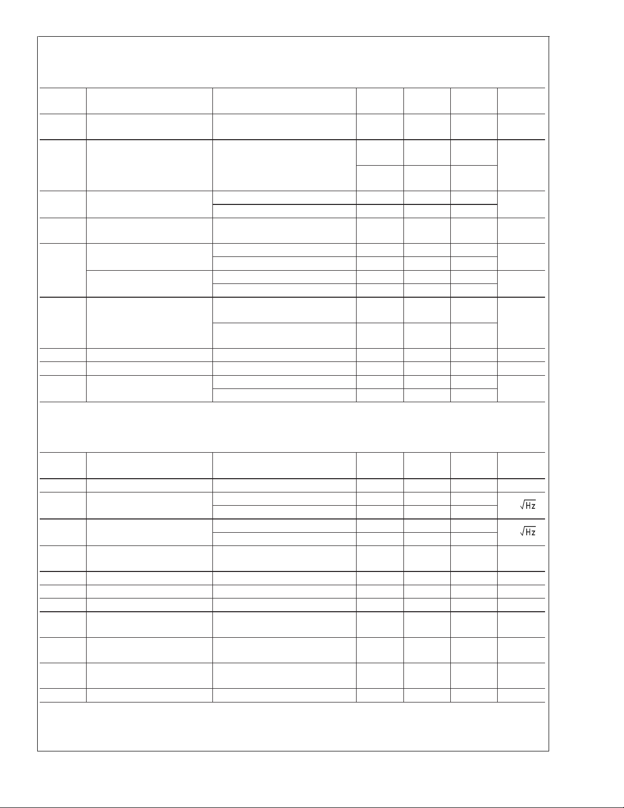
2.7V Electrical Characteristics
Unless otherwise specified, all limits guaranteed for at TJ= 25˚C, V+= 2.7V, V−= 0V, VCM=VO=V+/2, and Rf=2kΩ, and R
=1kΩto V+/2. Boldface limits apply at the temperature extremes.
Symbol Parameter Conditions Min
(Note 6)
BW −3dB BW A
e
n
Input-Referred Voltage Noise f = 100kHz 17
V
V
CM
= +1, V
= 0.7V
= 200mVPP,
OUT
f = 1kHz 25
i
n
Input-Referred Current Noise f = 100kHz 0.75
f = 1kHz 1.20
CT Rej. Cross-Talk Rejection
(LMH6646 only)
SR Slew Rate A
f = 5MHz, Receiver:
R
= 510Ω,AV=+2
f=Rg
= −1, VO=2V
V
PP
(Note 8, 13)
T
ON
Turn-On Time
(LMH6647 only)
T
OFF
Turn-Off Time
(LMH6647 only)
TH
SD
Shutdown Threshold
IS≤ 50µA 1.95 2.30
(LMH6647 only)
I
SD
Shutdown Pin Input Current
(Note 7) −20 µA
(LMH6647 only)
V
OS
TC V
I
B
I
OS
R
IN
Input Offset Voltage 0V ≤ VCM≤ 2.7V −3
Input Offset Average Drift (Note 12)
OS
Input Bias Current VCM= 2.5V (Note 7) 0.40 2
= 0.5V (Note 7) −0.68 −2
V
CM
Input Offset Current 0V ≤ VCM≤ 2.7V 1 500 nA
Common Mode Input
Resistance
C
IN
Common Mode Input
Capacitance
CMVR Input Common-Mode Voltage
CMRR ≥ 50dB −0.5 −0.3
Range
40 55 MHz
15 22 V/µs
−4
3.0
2.8
Typ
(Note 5)
Max
(Note 6)
Units
nV/
pA/
47 dB
250 ns
560 ns
±
13
4
±
5 µV/˚C
2.2
−2.2
3MΩ
2pF
−0.1
3.2
L
V
mV
µA
V
www.national.com3
Page 4
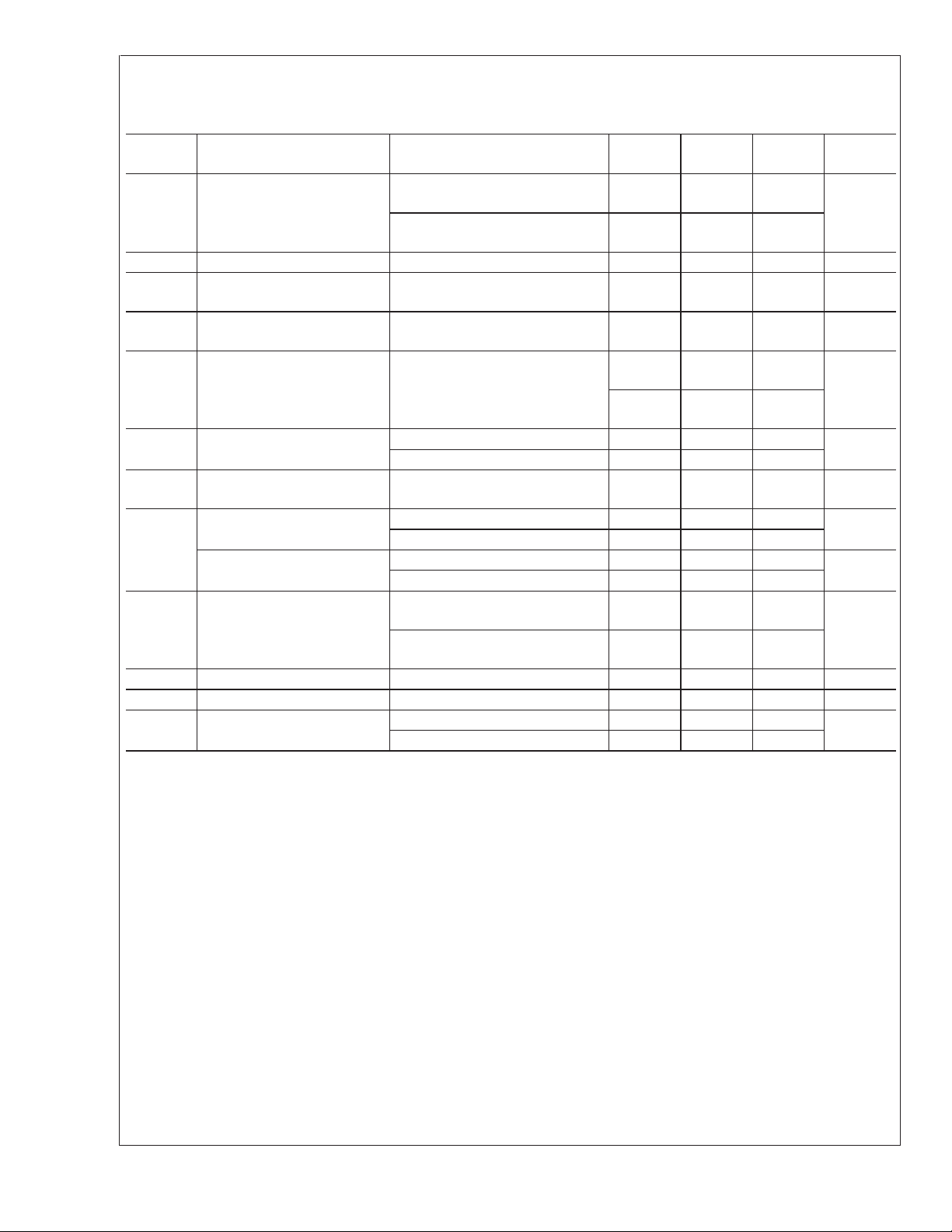
2.7V Electrical Characteristics (Continued)
Unless otherwise specified, all limits guaranteed for at TJ= 25˚C, V+= 2.7V, V−= 0V, VCM=VO=V+/2, and Rf=2kΩ, and R
=1kΩto V+/2. Boldface limits apply at the temperature extremes.
Symbol Parameter Conditions Min
LMH6645/46/47
CMRR Common Mode Rejection
Ratio
A
VOL
V
O
Large Signal Voltage Gain VO= 0.35V to 2.35V 76
Output Swing
High
Output Swing
Low
I
I
SC
OUT
Output Short Circuit Current Sourcing to V
Output Current V
PSRR Power Supply Rejection Ratio V
I
S
Supply Current (per channel) Normal Operation 650 1250
V
Stepped from 0V to 2.7V 46 77
CM
Stepped from 0V to 1.55V 58 76
V
CM
RL=1ktoV+/2 2.55 2.66
= 10k to V+/2 2.68
R
L
R
=1ktoV+/2 40 150
L
= 10k to V+/2 20
R
L
−
VID= 200mV (Note 10)
Sinking to V
+
VID= −200mV (Note 10)
= 0.5V from rails
OUT
+
= 2.7V to 3.7V or
−
=0Vto−1V
V
Shutdown Mode (LMH6647 only) 15 50
(Note 6)
74
75 83 dB
Typ
(Note 5)
Max
(Note 6)
87 dB
43
42
±
20 mA
L
Units
dB
V
mV
mA
µA
5V Electrical Characteristics
Unless otherwise specified, all limits guaranteed for at TJ= 25˚C, V+= 5V, V−= 0V, VCM=VO=V+/2, and Rf=2kΩ, and R
=1kΩto V+/2. Boldface limits apply at the temperature extremes.
Symbol Parameter Conditions Min
(Note 6)
BW −3dB BW A
e
n
Input-Referred Voltage Noise f = 100kHz 17
= +1, V
V
OUT
= 200mV
PP
f = 1kHz 25
i
n
Input-Referred Current Noise f = 100kHz 0.75
f = 1kHz 1.20
CT Rej. Cross-Talk Rejection
(LMH6646 only)
SR Slew Rate A
f = 5MHz, Receiver:
R
= 510Ω,AV=+2
f=Rg
= −1, VO=2V
V
PP
(Note 8, 13)
T
T
TH
ON
OFF
SD
Turn-On Time (LMH6647 only) 210 ns
Turn-Off Time (LMH6647 only) 500 ns
Shutdown Threshold
IS≤ 50µA 4.25 4.60 V
(LMH6647 only)
I
SD
Shutdown Pin Input Current
(Note 7)
(LMH6647 only)
V
OS
TC V
I
B
I
OS
R
IN
Input Offset Voltage 0V ≤ VCM≤ 5V −3
Input Offset Average Drift (Note 12)
OS
Input Bias Current VCM= 4.8V (Note 7)
= 0.5V (Note 7)
V
CM
Input Offset Current 0V ≤ VCM≤ 5V 1 500 nA
Common Mode Input
Resistance
40 55 MHz
15 22
−4
Typ
(Note 5)
Max
(Note 6)
nV/
pA/
47 dB
−20 µA
±
1
±
5 µV/C
+0.36
−0.68
3
4
+2
−2.2
−2
−2.2
3MΩ
L
Units
V/µs
mV
µA
www.national.com 4
Page 5
5V Electrical Characteristics (Continued)
Unless otherwise specified, all limits guaranteed for at TJ= 25˚C, V+= 5V, V−= 0V, VCM=VO=V+/2, and Rf=2kΩ, and R
=1kΩto V+/2. Boldface limits apply at the temperature extremes.
Symbol Parameter Conditions Min
(Note 6)
C
IN
Common Mode Input
Capacitance
CMVR Input Common-Mode Voltage
CMRR ≥ 50dB −0.5 −0.3
Range
CMRR Common Mode Rejection
Ratio
A
VOL
V
O
Large Signal Voltage Gain VO= 1.5V to 3.5V 76
Output Swing
High
Output Swing
Low
I
SC
Output Short Circuit Current Sourcing to V
Stepped from 0V to 5V 56 82
V
CM
Stepped from 0V to 3.8V 66 85
V
CM
RL=1ktoV+/2 4.80 4.95
= 10k to V+/2 4.98
R
L
R
=1ktoV+/2 50 200
L
= 10k to V+/2 20
R
L
−
VID= 200mV (Note 10)
Sinking to V
+
VID= −200mV (Note 10)
I
OUT
Output Current V
PSRR Power Supply Rejection Ratio V
I
S
Supply Current (per channel) Normal Operation 700 1400
= 0.5V From rails
OUT
+
=5Vto6VorV−= 0V to −1V 75 95 dB
Shutdown Mode (LMH6647 only) 10 50
5.3
5.1
74
Typ
(Note 5)
Max
(Note 6)
2pF
−0.1
5.5
85
55
53
±
20 mA
LMH6645/46/47
L
Units
V
dB
dB
V
mV
mA
µA
±
5V Electrical Characteristics
Unless otherwise specified, all limits guaranteed for at TJ= 25˚C, V+= 5V, V−= −5V, VCM=VO= 0V, Rf=2kΩ, and RL=
1kΩ to GND. Boldface limits apply at the temperature extremes.
Symbol Parameter Conditions Min
(Note 6)
BW −3dB BW A
e
n
Input-Referred Voltage Noise f = 100kHz 17
= +1, V
V
OUT
= 200mV
PP
40 55 MHz
Typ
(Note 5)
Max
(Note 6)
f = 1kHz 25
i
n
Input-Referred Current Noise f = 100kHz 0.75
f = 1kHz 1.20
CT Rej. Cross-Talk Rejection
(LMH6646 only)
SR Slew Rate A
T
T
TH
ON
OFF
SD
Turn-On Time (LMH6647 only) 200 ns
Turn-Off Time (LMH6647 only) 700 ns
Shutdown Threshold
(LMH6647 only)
I
SD
Shutdown Pin Input Current
f = 5MHz, Receiver:
R
= 510Ω,AV=+2
f=Rg
= −1, VO=2VPP(Note 8) 15 22 V/µs
V
IS≤ 50µA
47 dB
4.25 4.60
(Note 7) −20 µA
(LMH6647 only)
V
OS
TC V
Input Offset Voltage −5V ≤ VCM≤ 5V −3
Input Offset Average Drift (Note 12)
OS
−4
±
1
±
5 µV/˚C
3
4
Units
nV/
pA/
V
mV
www.national.com5
Page 6
±
5V Electrical Characteristics (Continued)
Unless otherwise specified, all limits guaranteed for at TJ= 25˚C, V+= 5V, V−= −5V, VCM=VO= 0V, Rf=2kΩ, and RL=
1kΩ to GND. Boldface limits apply at the temperature extremes.
Symbol Parameter Conditions Min
LMH6645/46/47
I
B
I
OS
R
IN
Input Bias Current VCM= 4.8V (Note 7)
= −4.5V (Note 7)
V
CM
Input Offset Current −5V ≤ VCM≤ 5V 3 500 nA
Common Mode Input
(Note 6)
Typ
(Note 5)
+0.40
−0.65
Max
(Note 6)
+2
+2.2
−2
−2.2
3MΩ
Resistance
C
IN
Common Mode Input
2pF
Capacitance
CMVR Input Common-Mode Voltage
Range
CMRR ≥ 50dB −5.5 −5.3
−5.1
5.3
5.5
5.1
CMRR Common Mode Rejection
Ratio
A
VOL
Large Signal Voltage Gain VO= −2V to 2V 76
Stepped from −5V to 5V 60 84
V
CM
Stepped from −5V to 3.5V 66 104
V
CM
85
74
V
O
I
SC
I
OUT
PSRR Power Supply Rejection Ratio V
I
S
Output Swing
High
Output Swing
Low
Output Short Circuit Current Sourcing to V
Output Current V
RL=1kΩ 4.70 4.92
= 10kΩ 4.97
R
L
R
=1kΩ −4.93 −4.70
L
= 10kΩ −4.98
R
L
VID= 200mV (Note 10)
Sinking to V
VID= −200mV (Note 10)
OUT
+
=5Vto6VorV−= −5V to −6V 76 95 dB
−
+
= 0.5V from rails
66
61
±
20 mA
Supply Current (per channel) Normal Operation 725 1600
Shutdown Mode (LMH6647 only) 10 50
Note 1: Absolute Maximum Ratings indicate limits beyond which damage to the device may occur. Operating Ratings indicate conditions for which the device is
intended to be functional, but specific performance is not guaranteed. For guaranteed specifications and the test conditions, see the Electrical Characteristics.
Note 2: Human body model, 1.5kΩ in series with 100pF.
Note 3: Applies to both single-supply and split-supply operation. Continuous short circuit operation at elevated ambient temperature can result in exceeding the
maximum allowed junction temperature of 150˚C.
Note 4: The maximum power dissipation is a function of T
=(T
P
D
J(MAX)-TA
Note 5: Typical values represent the most likely parametric norm.
Note 6: All limits are guaranteed by testing or statistical analysis.
Note 7: Positive current corresponds to current flowing into the device.
Note 8: Slew rate is the average of the rising and falling slew rates.
Note 9: Machine Model, 0Ω in series with 200pF.
Note 10: Short circuit test is a momentary test. See Note 11.
Note 11: Output short circuit duration is infinite for V
Note 12: Offset voltage average drift determined by dividing the change in V
Note 13: Guaranteed based on characterization only.
)/ θJA. All numbers apply for packages soldered directly onto a PC board.
<
6V at room temperature and below. For V
S
, θJA, and TA. The maximum allowable power dissipation at any ambient temperature is
J(MAX)
>
6V, allowable short circuit duration is 1.5ms.
at temperature extremes into the total temperature change.
OS
S
Units
µA
V
dB
dB
V
V
mA
µA
www.national.com 6
Page 7

LMH6645/46/47
Typical Performance Characteristics At T
Closed Loop Frequency Response for Various
Temperature Frequency Response for Various A
20020249
Open Loop Gain/Phase vs. Frequency for Various
Temperature THD vs. Output Swing
= 25˚C. Unless otherwise specified.
J
V
20020248
20020250 20020253
THD vs. Output Swing Output Swing vs. Frequency
20020254 20020255
www.national.com7
Page 8

Typical Performance Characteristics At T
Settling Time vs. Step Size Noise vs. Frequency
LMH6645/46/47
20020252 20020234
V
from V+vs. I
OUT
SOURCE
= 25˚C. Unless otherwise specified. (Continued)
J
V
from V−vs. I
OUT
SINK
20020237
20020238
Output Swing from V+vs. RL(tied to VS/2) Output Swing from V+vs. RL(tied to VS/2)
20020202 20020206
www.national.com 8
Page 9

LMH6645/46/47
Typical Performance Characteristics At T
Output Swing from V
Output Swing from V−vs. RL(tied to VS/2) Output Swing from V−vs. RL(tied to VS/2)
+
vs. RL(tied to VS/2) Output Swing from V−vs. RL(tied to VS/2)
20020204 20020203
= 25˚C. Unless otherwise specified. (Continued)
J
20020207
Cap Load Tolerance and Setting Time vs. Closed Loop
Gain Z
20020201 20020216
vs. Frequency
OUT
20020205
www.national.com9
Page 10

Typical Performance Characteristics At T
PSRR vs. Frequency CMRR vs. Frequency
LMH6645/46/47
= 25˚C. Unless otherwise specified. (Continued)
J
20020247
Crosstalk Rejection vs. Frequency (Output to Output)
(LMH6646) V
20020257
VOSvs. VS(A Typical Unit) VOSvs. V
Distribution
OS
(A Typical Unit)
OUT
20020251
20020225
20020218
www.national.com 10
20020228
Page 11

LMH6645/46/47
Typical Performance Characteristics At T
V
vs. V
OS
VOSvs. VCM(A Typical Unit) VOSvs. VCM(A Typical Unit)
(A Typical Unit) VOSvs. VCM(A Typical Unit)
OUT
20020229 20020231
= 25˚C. Unless otherwise specified. (Continued)
J
IBvs. V
CM
20020230 20020232
IBvs. V
20020226 20020219
CM
www.national.com11
Page 12

Typical Performance Characteristics At T
I
vs. V
B
S
LMH6645/46/47
20020227 20020223
IS(mA) (per channel) ISvs. V
= 25˚C. Unless otherwise specified. (Continued)
J
ISvs. V
CM
SHUTDOWN
(LMH6647)
20020224 20020221
ISvs. V
SHUTDOWN
(LMH6647) ISvs. V
20020220
www.national.com 12
SHUTDOWN
(LMH6647)
20020222
Page 13

LMH6645/46/47
Typical Performance Characteristics At T
= 25˚C. Unless otherwise specified. (Continued)
J
Shutdown Pin and Supply Current vs. Shutdown Voltage Small Signal Step Response
20020208
Large Signal Step Response Large Signal Step Response
20020243
Output Overload Recovery
20020244 20020245
20020246
www.national.com13
Page 14

Application Notes
Circuit Description:
The LMH6645/6646/6647 family is based on National Semiconductor’s proprietary VIP10 dielectrically isolated bipolar
process.
LMH6645/46/47
This device family architecture features the following:
Complimentary bipolar devices with exceptionally high f
•
(∼8GHz) even under low supply voltage (2.7V) and low
Collector bias current.
Rail-to-Rail input which allows the input common mode
•
voltage to go beyond either rail by about 0.5V typically.
A class A-B “turn-around” stage with improved noise,
•
offset, and reduced power dissipation compared to similar speed devices (patent pending).
Common Emitter push-pull output stage capable of 20mA
•
output current (at 0.5V from the supply rails) while consuming only ∼700µA of total supply current per channel.
This architecture allows output to reach within milli-volts
of either supply rail at light loads.
Consistent performance from any supply voltage
•
(2.7V-10V) with little variation with supply voltage for the
most important specifications (e.g. BW, SR, I
Application Hints:
The total input common mode voltage range, which extends
from below V
a NPN stage. The NPN stage is switched on whenever the
input is less than 1.2V from V
rest of the range. In terms of the input voltage, there is an
overlapping region where both stages are processing the
input signal. This region is about 0.5V from beginning to the
end. As far as the device application is concerned, this
transition is a transparent operation. However, keep in mind
that the input bias current value and direction will depend on
which input stage is operating (see typical performance
characteristics for plots). For low distortion applications, it is
best to keep the input common mode voltage from transversing this transition point. Low gain settling applications, which
generally encounter larger peak-to-peak input voltages,
could be configured as inverting stages to eliminate common
mode voltage fluctuations.
In terms of the output, when the output swing approaches
either supply rail, the output transistor will enter a
Quasi-saturated state. A subtle effect of this operational
region is that there is an increase in supply current in this
state (up to 1mA). The onset of Quasi-saturation region is a
function of output loading (current) and varies from 100mV at
no load to about 1V when output is delivering 20mA, as
measured from supplies. Both input common mode voltage
and output voltage level effect the supply current (see typical
performance characteristics for plot).
With 2.7V supplies and a common mode input voltage range
that extends beyond either supply rail, the
LMH6645/6646/6647 family is well suited to many low
voltage/low power applications. Even with 2.7V supplies, the
−
to beyond V+, is covered by both a PNP and
+
and the PNP stage covers the
OUT
, etc.)
−3dB BW (
@
AV= +1) is typically 55MHz with a tested limit
of 45MHz. Production testing guarantees that process variations will not compromise speed.
This device family is designed to avoid output phase reversal. With input over-drive, the output is kept near the supply
t
rail (or as close to it as mandated by the closed loop gain
setting and the input voltage).
Figure 1
, below, shows the
input and output voltage when the input voltage significantly
exceeds the supply voltages:
20020233
FIGURE 1. Input/Output Shown with Exceeded Input
CMVR
As can be seen, the output does not exhibit any phase
reversal as some op amps do. However, if the input voltage
range is exceeded by more than a diode drop beyond either
rail, the internal ESD protection diodes will start to conduct.
The current flow in these ESD diodes should be externally
limited.
LMH6647
Micro-power Shutdown
The LMH6647 can be shutdown to save power and reduce
its supply current to less than 50µAguaranteed, by applying
a voltage to the SD pin. The SD pin is “active high” and
needs to be tied to V
current (
to V
<
20µA, 4pF equivalent capacitance) and a resistor
−
(≤20kΩ) will result in normal operation. Shutdown is
guaranteed when SD pin is 0.4V or less from V
−
for normal operation. This input is low
+
at any
operating supply voltage and temperature.
In the shutdown mode, essentially all internal device biasing
is turned off in order to minimize supply current flow and the
output goes into Hi-Z (high impedance) mode. Complete
device Turn-on and Turn-off times vary considerably relative
to the output loading conditions, output voltage, and input
impedance, but is generally limited to less than 1µs (see
tables for actual data).
www.national.com 14
Page 15

Application Notes (Continued)
During shutdown, the input stage has an equivalent circuit as
shown below in
FIGURE 2. LMH6647 Equivalent Input in Shutdown
As can be seen above, in shutdown, there may be current
flow through the internal diodes shown, caused by input
potential, if present. This current may flow through the external feedback resistor and result in an apparent output signal.
In most shutdown applications the presence of this output is
inconsequential. However, if the output is “forced” by another
device such as in a multiplexer, the other device will need to
conduct the current described in order to maintain the output
potential.
To keep the output at or near ground during shutdown when
there is no other device to hold the output low, a switch
(transistor) could be used to shunt the output to ground.
Figure 3
the output near ground (∼80mV):
Figure 2
20020256
Mode
shows a circuit where a NPN bipolar is used to keep
Figure 4
shows the output waveform.
20020236
FIGURE 4. Output Held Low by Active Pull-Down
Circuit
If bipolar transistor power dissipation is not tolerable, the
switch could be by a N-channel enhancement mode MOSFET.
2.7V Single Supply RRIO 2:1 MUX:
The schematic show in
Figure 5
will function as a 2:1 MUX
operating on a single 2.7V power supply, by utilizing the
shutdown feature of the LMH6647:
LMH6645/46/47
20020264
FIGURE 3. Active Pull-Down Schematic
20020258
FIGURE 5. 2:1 MUX Operating off a 2.7V Single Supply
www.national.com15
Page 16

Application Notes (Continued)
Figure 6
1MHz sine and a 250KHz triangular waveform.
LMH6645/46/47
As can be seen in
there are no spikes or glitches due to the switching. Switching times are approximately around 500ns based on the time
when the output is considered “valid”.
Printed Circuit Board Layout, Component Values Selection, and Evaluation Boards:
Generally, a good high-frequency layout will keep power
supply and ground traces away from the inverting input and
output pins. Parasitic capacitances on these nodes to
shows the MUX output when selecting between a
20020235
FIGURE 6. 2:1 MUX Output
Figure 6
, the output is well behaved and
ground will cause frequency response peaking and possible
circuit oscillations (see Application Note OA-15 for more
information).
Another important parameter in working with high
speed/high performance amplifiers, is the component values
selection. Choosing large valued external resistors, will effect the closed loop behavior of the stage because of the
interaction of these resistors with parasitic capacitances.
These capacitors could be inherent to the device or a
by-product of the board layout and component placement.
Either way, keeping the resistor values lower, will diminish
this interaction. On the other hand, choosing very low value
resistors could load down nodes and will contribute to higher
overall power dissipation.
National Semiconductor suggests the following evaluation
boards as a guide for high frequency layout and as an aid in
device testing and characterization:
Device Package Evaluation
Board PN
LMH6645MF SOT23-5 CLC730068
LMH6645MA 8-Pin SOIC CLC730027
LMH6646MA 8-Pin SOIC CLC730036
LMH6646MM 8-Pin MSOP CLC730123
LMH6647MA 8-Pin SOIC CLC730027
LMH6647MF SOT23-6 CLC730116
These free evaluation boards are shipped when a device
sample request is placed with National Semiconductor.
LMH6647 Evaluation:
For normal operation, tie the SD pin to V
−
.
www.national.com 16
Page 17

Physical Dimensions inches (millimeters) unless otherwise noted
LMH6645/46/47
5-Pin SOT23
NS Package Number MF05A
6-Pin SOT23
NS Package Number MF06A
www.national.com17
Page 18

Physical Dimensions inches (millimeters) unless otherwise noted (Continued)
LMH6645/46/47
8-Pin SOIC
NS Package Number M08A
8Pin MSOP
NS Package Number MUA08A
www.national.com 18
Page 19

Notes
LMH6645/46/47 2.7V, 650µA, 55MHz, Rail-to-Rail Input and Output Amplifiers with Shutdown
Option
LIFE SUPPORT POLICY
NATIONAL’S PRODUCTS ARE NOT AUTHORIZED FOR USE AS CRITICAL COMPONENTS IN LIFE SUPPORT
DEVICES OR SYSTEMS WITHOUT THE EXPRESS WRITTEN APPROVAL OF THE PRESIDENT AND GENERAL
COUNSEL OF NATIONAL SEMICONDUCTOR CORPORATION. As used herein:
1. Life support devices or systems are devices or
systems which, (a) are intended for surgical implant
into the body, or (b) support or sustain life, and
whose failure to perform when properly used in
accordance with instructions for use provided in the
2. A critical component is any component of a life
support device or system whose failure to perform
can be reasonably expected to cause the failure of
the life support device or system, or to affect its
safety or effectiveness.
labeling, can be reasonably expected to result in a
significant injury to the user.
National Semiconductor
Corporation
Americas
Email: support@nsc.com
www.national.com
National does not assume any responsibility for use of any circuitry described, no circuit patent licenses are implied and National reserves the right at any time without notice to change said circuitry and specifications.
National Semiconductor
Europe
Fax: +49 (0) 180-530 85 86
Email: europe.support@nsc.com
Deutsch Tel: +49 (0) 69 9508 6208
English Tel: +44 (0) 870 24 0 2171
Français Tel: +33 (0) 1 41 91 8790
National Semiconductor
Asia Pacific Customer
Response Group
Tel: 65-2544466
Fax: 65-2504466
Email: ap.support@nsc.com
National Semiconductor
Japan Ltd.
Tel: 81-3-5639-7560
Fax: 81-3-5639-7507
 Loading...