

Page 1
LMH6642/6643/6644
3V, Low Power, 130MHz, 75mA Rail-to-Rail Output
Amplifiers
General Description
The LMH664X family true single supply voltage feedback
amplifiers offer high speed (130MHz), low distortion
(−62dBc), and exceptionally high output current (approximately 75mA) at low cost and with reduced power consumption when compared against existing devices with similar
performance.
Input common mode voltage range extends to 0.5V below V
and 1V from V+. Output voltage range extends to within
40mV of either supply rail, allowing wide dynamic range
especially desirable in low voltage applications. The output
stage is capable of approximately 75mA in order to drive
heavy loads. Fast output Slew Rate (130V/µs) ensures large
peak-to-peak output swings can be maintained even at
higher speeds, resulting in exceptional full power bandwidth
of 40MHz with a 3V supply. These characteristics, along with
low cost, are ideal features for a multitude of industrial and
commercial applications.
Careful attention has been paid to ensure device stability
under all operating voltages and modes. The result is a very
well behaved frequency response characteristic (0.1dB gain
flatness up the 12MHz under 150Ω load and A
minimal peaking (typically 2dB maximum) for any gain setting and under both heavy and light loads. This along with
fast settling time (68ns) and low distortion allows the device
to operate well in ADC buffer, and high frequency filter
applications as well as other applications.
This device family offers professional quality video performance with low DG (0.01%) and DP (0.01˚) characteristics.
Differential Gain and Differential Phase characteristics are
also well maintained under heavy loads (150Ω) and throughout the output voltage range. The LMH664X family is offered
= +2) with
V
in single (LMH6642), dual (LMH6643), and quad (LMH6644)
options. See ordering information for packages offered.
Features
(VS=±5V, TA= 25˚C, RL=2kΩ,AV= +1. Typical values
unless specified).
n −3dB BW (A
−
n Supply voltage range 3V to 12.8V
n Slew rate (Note 8), (A
n Supply current (no load) 2.7mA/amp
n Output short circuit current +115mA/−145mA
n Linear output current
n Input common mode volt. 0.5V beyond V
n Output voltage swing 40mV from rails
n Input voltage noise (100kHz) 17nV/
n Input current noise (100kHz) 0.9pA/
n THD (5MHz, RL=2kΩ,VO=2VPP,AV= +2) −62dBc
n Settling time 68ns
n Fully characterized for 3V, 5V, and
n Overdrive recovery 100ns
n Output short circuit protected (Note 11)
n No output phase reversal with CMVR exceeded
= +1) 130MHz
V
= −1) 130V/µs
V
±
5V
Applications
n Active filters
n CD/DVD ROM
n ADC buffer amp
n Portable video
n Current sense buffer
May 2003
±
75mA
−
, 1V from V
LMH6642/6643/6644 3V, Low Power, 130MHz, 75mA Rail-to-Rail Output Amplifiers
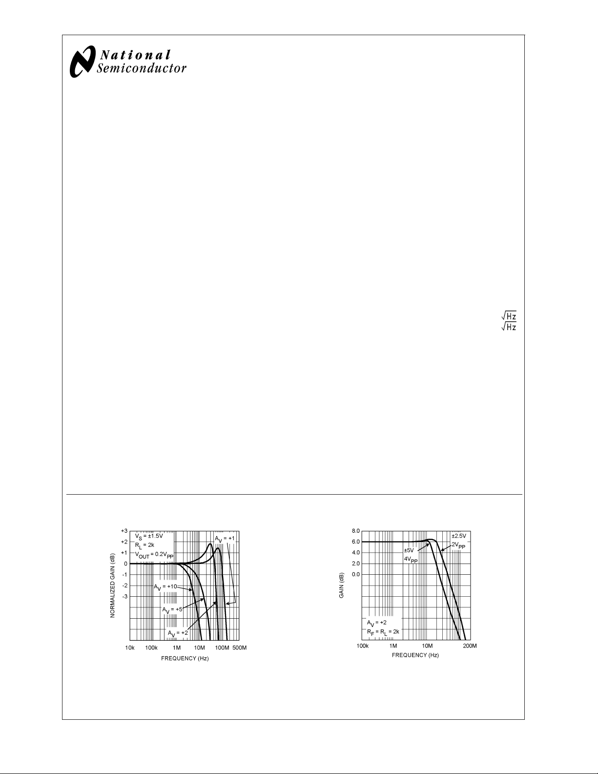
+
Closed Loop Gain vs. Frequency for Various Gain Large Signal Frequency Response
20018535
© 2003 National Semiconductor Corporation DS200185 www.national.com
20018547
Page 2
Absolute Maximum Ratings (Note 1)
If Military/Aerospace specified devices are required,
Infrared or Convection Reflow(20 sec) 235˚C
Wave Soldering Lead Temp.(10 sec) 260˚C
please contact the National Semiconductor Sales Office/
Distributors for availability and specifications.
Operating Ratings (Note 1)
ESD Tolerance 2KV (Note 2)
LMH6642/6643/6644
Differential
V
IN
Output Short Circuit Duration (Note 3), (Note 11)
Supply Voltage (V
Voltage at Input/Output pins V
+-V−
) 13.5V
+
+0.8V, V−−0.8V
Input Current
Storage Temperature Range −65˚C to +150˚C
Junction Temperature (Note 4) +150˚C
Soldering Information
200V (Note 9)
±
2.5V
±
10mA
Supply Voltage (V
Junction Temperature Range (Note 4) −40˚C to +85˚C
Package Thermal Resistance (Note 4) (θ
SOT23-5 265˚C/W
SOIC-8 190˚C/W
MSOP-8 235˚C/W
SOIC-14 145˚C/W
TSSOP-14 155˚C/W
+–V−
) 3V to 12.8V
)
JA
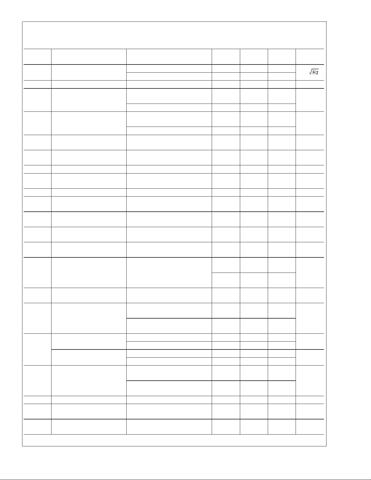
3V Electrical Characteristics
Unless otherwise specified, all limits guaranteed for at TJ= 25˚C, V+= 3V, V−= 0V, VCM=VO=V+/2, and RL=2kΩ to V+/2.
Boldface limits apply at the temperature extremes.
Symbol Parameter Conditions Min
(Note 6)
BW −3dB BW A
BW
0.1dB
0.1dB Gain Flatness AV= +2, RL= 150Ω to V+/2,
PBW Full Power Bandwidth A
e
n
Input-Referred Voltage Noise f = 100kHz 17
= +1, V
V
A
= +2, −1, V
V
= 402Ω,V
R
L
= +1, −1dB, V
V
OUT
= 200mV
OUT
= 200mV
OUT
OUT
PP
= 200mV
=1V
PP
PP
PP
f = 1kHz 48
i
n
Input-Referred Current Noise f = 100kHz 0.90
f = 1kHz 3.3
THD Total Harmonic Distortion f = 5MHz, V
= 100Ω to V+/2
R
L
DG Differential Gain V
DP Differential Phase V
= 1V, NTSC, AV=+2
CM
=150Ω to V+/2
R
L
R
=1kΩ to V+/2 0.03
L
= 1V, NTSC, AV=+2
CM
=150Ω to V+/2
R
L
R
=1kΩ to V+/2 0.03
L
=2VPP,AV= −1,
O
CT Rej. Cross-Talk Rejection f = 5MHz, Receiver:
= 510Ω,AV=+2
f=Rg
=5V
S
= −1, VI=2V
V
PP
T
S
Settling Time VO=2VPP,±0.1%, 8pF Load,
SR Slew Rate (Note 8) A
V
OS
TC V
I
B
I
OS
R
IN
Input Offset Voltage
Input Offset Average Drift (Note 12)
OS
Input Bias Current (Note 7) −1.50 −2.60
Input Offset Current 20 800
Common Mode Input
R
V
Resistance
C
IN
Common Mode Input
Capacitance
80 115
90 120 V/µs
Typ
(Note 5)
Max
(Note 6)
46
19 MHz
40 MHz
−48
0.17
0.05
47 dB
68 ns
±
1
±
5 µV/˚C
±
5
±
7
−3.25
1000
3MΩ
2pF
Units
MHz
nV/
pA/
dBc
%
deg
mV
µA
nA
www.national.com 2
Page 3
3V Electrical Characteristics (Continued)
Unless otherwise specified, all limits guaranteed for at TJ= 25˚C, V+= 3V, V−= 0V, VCM=VO=V+/2, and RL=2kΩ to V+/2.
Boldface limits apply at the temperature extremes.
Symbol Parameter Conditions Min
(Note 6)
CMVR Input Common-Mode Voltage
CMRR ≥ 50dB −0.5 −0.2
Range
CMRR Common Mode Rejection
Stepped from 0V to 1.5V 72 95 dB
V
CM
Ratio
A
VOL
V
O
I
SC
I
OUT
+PSRR Positive Power Supply
Large Signal Voltage Gain VO= 0.5V to 2.5V
=2kΩ to V+/2
R
L
V
= 0.5V to 2.5V
O
= 150Ω to V+/2
R
L
Output Swing
High
Output Swing
Low
RL=2kΩ to V+/2, VID= 200mV 2.90 2.98
R
= 150Ω to V+/2, VID= 200mV 2.80 2.93
L
R
=2kΩ to V+/2, VID= −200mV 25 75
L
R
= 150Ω to V+/2, VID= −200mV 75 150
L
Output Short Circuit Current Sourcing to V+/2
= 200mV (Note 10)
V
Output Current V
ID
Sinking to V
= −200mV (Note 10)
V
ID
OUT
+
V
= 3.0V to 3.5V, VCM= 1.5V 75 85 dB
+
/2
= 0.5V from either supply
Rejection Ratio
I
S
Supply Current (per channel) No Load 2.70 4.00
1.8
1.6
80
75
74
70
50
35
55
40
Typ
(Note 5)
Max
(Note 6)
−0.1
2.0
96
82
95
110
±
65 mA
4.50
Units
LMH6642/6643/6644
V
dB
V
mV
mA
mA
5V Electrical Characteristics
Unless otherwise specified, all limits guaranteed for at TJ= 25˚C, V+= 5V, V−= 0V, VCM=VO=V+/2, and RL=2kΩ to V+/2.
Boldface limits apply at the temperature extremes.
Symbol Parameter Conditions Min
(Note 6)
BW −3dB BW A
BW
0.1dB
0.1dB Gain Flatness AV= +2, RL= 150Ω to V+/2,
PBW Full Power Bandwidth A
e
n
Input-Referred Voltage Noise f = 100kHz 17
= +1, V
V
A
= +2, −1, V
V
= 402Ω,V
R
f
= +1, −1dB, V
V
OUT
OUT
= 200mV
= 200mV
OUT
= 200mV
OUT
PP
=2V
90 120
PP
PP
PP
f = 1kHz 48
i
n
Input-Referred Current Noise f = 100kHz 0.90
f = 1kHz 3.3
THD Total Harmonic Distortion f = 5MHz, V
DG Differential Gain NTSC, A
=150Ω to V+/2
R
L
R
=1kΩ to V+/2 0.05
L
DP Differential Phase NTSC, A
=150Ω to V+/2
R
L
R
=1kΩ to V+/2 0.01
L
=2VPP,AV= +2 −60 dBc
O
=+2
V
=+2
V
CT Rej. Cross-Talk Rejection f = 5MHz, Receiver:
R
T
S
Settling Time VO=2VPP,±0.1%, 8pF Load 68 ns
= 510Ω,AV=+2
f=Rg
Typ
(Note 5)
Max
(Note 6)
46
15 MHz
22 MHz
0.16
0.05
47 dB
Units
nV/
pA/
MHz
%
deg
www.national.com3
Page 4
5V Electrical Characteristics (Continued)
Unless otherwise specified, all limits guaranteed for at TJ= 25˚C, V+= 5V, V−= 0V, VCM=VO=V+/2, and RL=2kΩ to V+/2.
Boldface limits apply at the temperature extremes.
Symbol Parameter Conditions Min
SR Slew Rate (Note 8) A
V
LMH6642/6643/6644
OS
TC V
I
B
I
OS
R
IN
Input Offset Voltage
Input Offset Average Drift (Note 12)
OS
Input Bias Current (Note 7)
Input Offset Current
Common Mode Input
= −1, VI=2V
V
PP
Resistance
C
IN
Common Mode Input
Capacitance
CMVR Input Common-Mode Voltage
CMRR ≥ 50dB
Range
CMRR Common Mode Rejection
Stepped from 0V to 3.5V
V
CM
Ratio
A
VOL
V
O
I
SC
I
OUT
+PSRR Positive Power Supply
Large Signal Voltage Gain VO= 0.5V to 4.50V
=2kΩ to V+/2
R
L
V
= 0.5V to 4.25V
O
= 150Ω to V+/2
R
L
Output Swing
High
Output Swing
Low
RL=2kΩ to V+/2, VID= 200mV 4.90 4.98
R
= 150Ω to V+/2, VID= 200mV 4.65 4.90
L
R
=2kΩ to V+/2, VID= −200mV 25 100
L
R
= 150Ω to V+/2, VID= −200mV 100 150
L
Output Short Circuit Current Sourcing to V+/2
= 200mV (Note 10)
V
ID
Sinking to V
= −200mV (Note 10)
V
ID
+
/2
Output Current VO= 0.5V from either supply
+
V
= 4.0V to 6V
Rejection Ratio
I
S
Supply Current (per channel) No Load
(Note 6)
95 125 V/µs
3.8
3.6
72 95
86
82
76
72
55
40
70
55
79 90
Typ
(Note 5)
±
1
±
5 µV/˚C
−1.70
20
Max
(Note 6)
±
5
±
7
−2.60
−3.25
800
1000
3
2
−0.5
−0.2
−0.1
4.0
98
82
115
140
±
70 mA
2.70
4.25
5.00
Units
mV
µA
nA
MΩ
pF
V
dB
dB
V
mV
mA
dB
mA
±
5V Electrical Characteristics
Unless otherwise specified, all limits guaranteed for at TJ= 25˚C, V+= 5V, V−= −5V, VCM=VO= 0V and RL=2kΩ to ground.
Boldface limits apply at the temperature extremes.
Symbol Parameter Conditions Min
(Note 6)
BW −3dB BW A
BW
0.1dB
0.1dB Gain Flatness AV= +2, RL= 150Ω to V+/2,
PBW Full Power Bandwidth A
e
n
Input-Referred Voltage Noise f = 100kHz 17
= +1, V
V
A
= +2, −1, V
V
= 806Ω,V
R
f
= +1, −1dB, V
V
OUT
OUT
= 200mV
= 200mV
OUT
= 200mV
OUT
PP
=2V
95 130
PP
PP
PP
Typ
(Note 5)
Max
(Note 6)
46
12 MHz
24 MHz
f = 1kHz 48
www.national.com 4
Units
MHz
nV/
Page 5
±
5V Electrical Characteristics (Continued)
Unless otherwise specified, all limits guaranteed for at TJ= 25˚C, V+= 5V, V−= −5V, VCM=VO= 0V and RL=2kΩ to ground.
Boldface limits apply at the temperature extremes.
Symbol Parameter Conditions Min
(Note 6)
i
n
Input-Referred Current Noise f = 100kHz 0.90
f = 1kHz 3.3
THD Total Harmonic Distortion f = 5MHz, V
DG Differential Gain NTSC, A
=150Ω to V+/2
R
L
R
=1kΩ to V+/2 0.01
L
DP Differential Phase NTSC, A
=150Ω to V+/2
R
L
R
=1kΩ to V+/2 0.01
L
=2VPP,AV= +2 −62 dBc
O
=+2
V
=+2
V
CT Rej. Cross-Talk Rejection f = 5MHz, Receiver:
Rf=Rg= 510Ω,AV=+2
T
S
SR Slew Rate (Note 8) A
V
OS
TC V
I
B
I
OS
R
IN
Settling Time VO=2VPP,±0.1%, 8pF Load,
=5V
V
S
= −1, VI=2V
V
Input Offset Voltage
Input Offset Average Drift (Note 12)
OS
Input Bias Current (Note 7)
Input Offset Current
Common Mode Input
PP
100 135 V/µs
Resistance
C
IN
Common Mode Input
Capacitance
CMVR Input Common-Mode Voltage
CMRR ≥ 50dB
Range
3.8
3.6
CMRR Common Mode Rejection
Ratio
A
VOL
V
O
Large Signal Voltage Gain VO= −4.5V to 4.5V,
Output Swing
High
Output Swing
Low
I
I
SC
OUT
Output Short Circuit Current Sourcing to Ground
Output Current VO= 0.5V from either supply
PSRR Power Supply Rejection Ratio (V
I
S
Supply Current (per channel) No Load
Stepped from −5V to 3.5V
V
CM
74 95
88
=2kΩ
R
L
V
= −4.0V to 4.0V,
O
= 150Ω
R
L
84
78
74
RL=2kΩ,VID= 200mV 4.90 4.96
R
= 150Ω,VID= 200mV 4.65 4.80
L
R
=2kΩ,VID= −200mV −4.96 −4.90
L
R
= 150Ω,VID= −200mV −4.80 −4.65
L
60
= 200mV (Note 10)
V
ID
Sinking to Ground
= −200mV (Note 10)
V
ID
+,V−
) = (4.5V, −4.5V) to (5.5V,
−5.5V)
35
85
65
±
75 mA
78 90
Typ
(Note 5)
Max
(Note 6)
0.15
0.04
47 dB
68
±
±
1
±
5 µV/˚C
−1.60
20
5
±
7
−2.60
−3.25
800
1000
3
2
−5.5
−5.2
−5.1
4.0
96
82
115
145
2.70
4.50
5.50
Units
pA/
deg
ns
mV
µA
nA
MΩ
pF
dB
dB
mA
dB
mA
LMH6642/6643/6644
%
V
V
V
www.national.com5
Page 6
±
5V Electrical Characteristics (Continued)
Note 1: Absolute Maximum Ratings indicate limits beyond which damage to the device may occur. Operating Ratings indicate conditions for which the device is
intended to be functional, but specific performance is not guaranteed. For guaranteed specifications and the test conditions, see the Electrical Characteristics.
Note 2: Human body model, 1.5kΩ in series with 100pF.
Note 3: Applies to both single-supply and split-supply operation. Continuous short circuit operation at elevated ambient temperature can result in exceeding the
maximum allowed junction temperature of 150˚C.
Note 4: The maximum power dissipation is a function of T
P
=(T
D
LMH6642/6643/6644
J(MAX)-TA
Note 5: Typical values represent the most likely parametric norm.
Note 6: All limits are guaranteed by testing or statistical analysis.
Note 7: Positive current corresponds to current flowing into the device.
Note 8: Slew rate is the average of the rising and falling slew rates.
Note 9: Machine Model, 0Ω in series with 200pF.
Note 10: Short circuit test is a momentary test. See Note 11.
Note 11: Output short circuit duration is infinite for V
Note 12: Offset voltage average drift determined by dividing the change in V
)/ θJA. All numbers apply for packages soldered directly onto a PC board.
<
6V at room temperature and below. For V
S
, θJA, and TA. The maximum allowable power dissipation at any ambient temperature is
J(MAX)
>
6V, allowable short circuit duration is 1.5ms.
at temperature extremes by the total temperature change.
OS
S
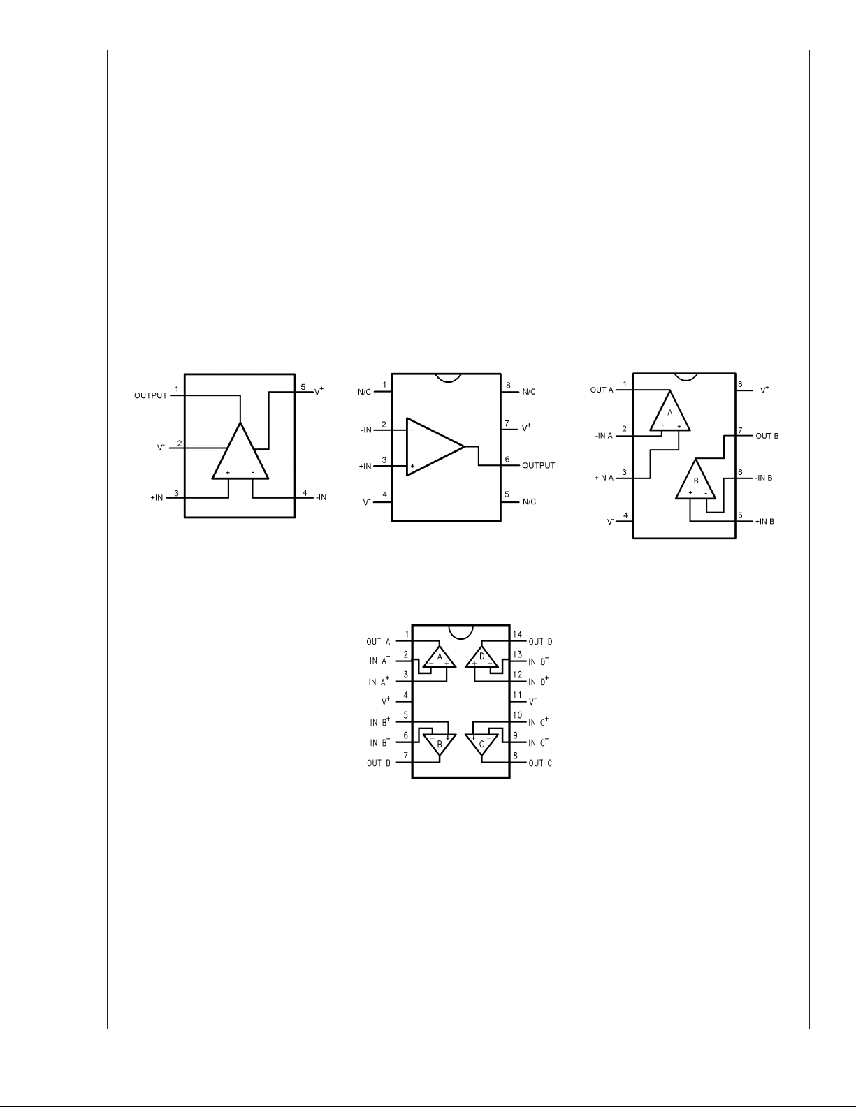
Connection Diagrams
SOIC-8 and MSOP-8
SOT23-5 (LMH6642) SOIC-8 (LMH6642)
(LMH6643)
Top View
20018561
Top View
SOIC-14 and TSSOP-14
(LMH6644)
Top View
20018562
20018563
Top View
20018568
www.national.com 6
Page 7
LMH6642/6643/6644
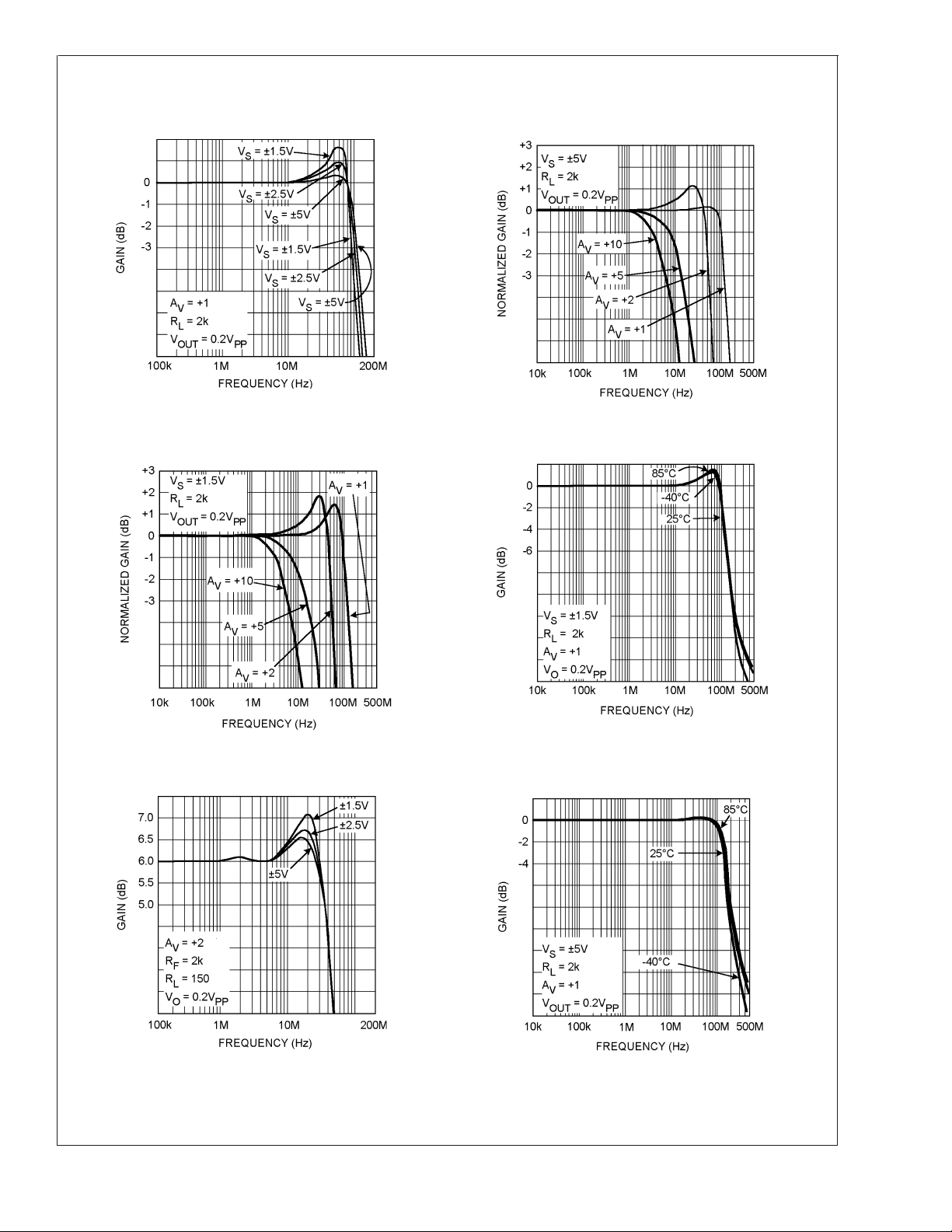
Typical Performance Characteristics At T
= 25˚C, V+= +5, V−= −5V, RF=RL=2kΩ. Unless
J
otherwise specified.
Closed Loop Frequency Response for Various Supplies Closed Loop Gain vs. Frequency for Various Gain
20018557
20018551
Closed Loop Frequency Response for Various
Closed Loop Gain vs. Frequency for Various Gain
Temperature
20018535
Closed Loop Gain vs. Frequency for Various Supplies
20018548
20018550
Closed Loop Frequency Response for Various
Temperature
20018534
www.national.com7
Page 8

Typical Performance Characteristics At T
otherwise specified. (Continued)
Large Signal Frequency Response
LMH6642/6643/6644
= 25˚C, V+= +5, V−= −5V, RF=RL=2kΩ. Unless
J
Closed Loop Small Signal Frequency Response for
Various Supplies
20018547
Closed Loop Frequency Response for Various Supplies
20018544
V
OUT(VPP
) for THD<0.5% V
±
0.1dB Gain Flatness for Various Supplies
OUT(VPP
) for THD<0.5%
20018546
20018545
20018509 20018508
www.national.com 8
Page 9

LMH6642/6643/6644
Typical Performance Characteristics At T
= 25˚C, V+= +5, V−= −5V, RF=RL=2kΩ. Unless
J
otherwise specified. (Continued)
V
OUT(VPP
) for THD<0.5% Open Loop Gain/Phase for Various Temperature
20018510
Open Loop Gain/Phase for Various Temperature HD2 (dBc) vs. Output Swing
20018532
20018533
HD3 (dBc) vs. Output Swing HD2 vs. Output Swing
20018515
20018514
20018504
www.national.com9
Page 10

Typical Performance Characteristics At T
otherwise specified. (Continued)
HD3 vs. Output Swing THD (dBc) vs. Output Swing
LMH6642/6643/6644
20018505 20018506
Settling Time vs. Input Step Amplitude
(Output Slew and Settle Time) Input Noise vs. Frequency
= 25˚C, V+= +5, V−= −5V, RF=RL=2kΩ. Unless
J
20018513
V
from V+vs. I
OUT
www.national.com 10
SOURCE
20018518 20018519
V
OUT
from V−vs. I
20018512
SINK
Page 11

LMH6642/6643/6644
Typical Performance Characteristics At T
otherwise specified. (Continued)
V
from V+vs. I
OUT
Swing vs. V
SOURCE
20018516 20018517
S
= 25˚C, V+= +5, V−= −5V, RF=RL=2kΩ. Unless
J
V
from V−vs. I
OUT
Short Circuit Current (to VS/2) vs. V
SINK
S
Output Sinking Saturation Voltage vs. I
20018529 20018531
OUT
20018520
Output Sourcing Saturation Voltage vs. I
OUT
20018501
www.national.com11
Page 12

Typical Performance Characteristics At T
otherwise specified. (Continued)
= 25˚C, V+= +5, V−= −5V, RF=RL=2kΩ. Unless
J
Closed Loop Output Impedance vs. Frequency A
LMH6642/6643/6644
CMRR vs. Frequency
= +1 PSRR vs. Frequency
V
20018502 20018503
Crosstalk Rejection vs. Frequency
(Output to Output)
20018507
VOSvs. V
www.national.com 12
(Typical Unit) VOSvs. VCM(Typical Unit)
OUT
20018530
20018511
20018527
Page 13

LMH6642/6643/6644
Typical Performance Characteristics At T
otherwise specified. (Continued)
V
vs. VS(for 3 Representative Units) VOSvs. VS(for 3 Representative Units)
OS
20018522 20018523
VOSvs. VS(for 3 Representative Units) IBvs. V
= 25˚C, V+= +5, V−= −5V, RF=RL=2kΩ. Unless
J
S
IOSvs. V
20018524
S
20018526
ISvs. V
CM
20018525
20018528
www.national.com13
Page 14

Typical Performance Characteristics At T
otherwise specified. (Continued)
I
vs. V
S
S
LMH6642/6643/6644
20018521
Large Signal Step Response Large Signal Step Response
= 25˚C, V+= +5, V−= −5V, RF=RL=2kΩ. Unless
J
Small Signal Step Response
20018553
20018541 20018539
Small Signal Step Response Small Signal Step Response
20018556 20018536
www.national.com 14
Page 15

LMH6642/6643/6644
Typical Performance Characteristics At T
otherwise specified. (Continued)
Small Signal Step Response Small Signal Step Response
20018552
Large Signal Step Response Large Signal Step Response
= 25˚C, V+= +5, V−= −5V, RF=RL=2kΩ. Unless
J
20018538
Large Signal Step Response
20018537 20018554
20018560
www.national.com15
Page 16

Application Notes
CIRCUIT DESCRIPTION:
The LMH664X family is based on National Semiconductor’s
proprietary VIP10 dielectrically isolated bipolar process.
This device family architecture features the following:
Complimentary bipolar devices with exceptionally high f
•
LMH6642/6643/6644
(∼8GHz) even under low supply voltage (2.7V) and low
bias current.
A class A-B “turn-around” stage with improved noise,
•
offset, and reduced power dissipation compared to similar speed devices (patent pending).
Common Emitter push-push output stage capable of
•
75mA output current (at 0.5V from the supply rails) while
consuming only 2.7mA of total supply current per channel. This architecture allows output to reach within millivolts of either supply rail.
Consistent performance from any supply voltage (3V-
•
10V) with little variation with supply voltage for the most
important specifications (e.g. BW, SR, I
Significant power saving (∼40%) compared to competi-
•
OUT
tive devices on the market with similar performance.
Application Hints:
This Op Amp family is a drop-in replacement for the AD805X
family of high speed Op Amps in most applications. In addition, the LMH664X will typically save about 40% on power
dissipation, due to lower supply current, when compared to
competition. All AD805X family’s guaranteed parameters are
included in the list of LMH664X guaranteed specifications in
order to ensure equal or better level of performance. However, as in most high performance parts, due to subtleties of
applications, it is strongly recommended that the performance of the part to be evaluated is tested under actual
operating conditions to ensure full compliance to all specifications.
With 3V supplies and a common mode input voltage range
that extends 0.5V below V
−
, the LMH664X find applications
in low voltage/low power applications. Even with 3V sup-
@
plies, the −3dB BW (
AV= +1) is typically 115MHz with a
tested limit of 80MHz. Production testing guarantees that
process variations with not compromise speed. High frequency response is exceptionally stable confining the typical
-3dB BW over the industrial temperature range to
As can be seen from the typical performance plots, the
LMH664X output current capability (∼75mA) is enhanced
compared to AD805X. This enhancement, increases the
output load range, adding to the LMH664X’s versatility.
Because of the LMH664X’s high output current capability
attention should be given to device junction temperature in
order not to exceed the Absolute Maximum Rating.
, etc.)
±
2.5%.
This device family was designed to avoid output phase
reversal. With input overdrive, the output is kept near supply
rail (or as closed to it as mandated by the closed loop gain
setting and the input voltage). See Figure 1:
t
20018542
FIGURE 1. Input and Output Shown with CMVR
Exceeded
+
However, if the input voltage range of −0.5V to 1V from V
is
exceeded by more than a diode drop, the internal ESD
protection diodes will start to conduct.The current in the
diodes should be kept at or below 10mA.
Output overdrive recovery time is less than 100ns as can be
seen from Figure 2 plot:
20018543
FIGURE 2. Overload Recovery Waveform
www.national.com 16
Page 17

Application Notes (Continued)
SINGLE SUPPLY, LOW POWER PHOTODIODE AMPLIFIER:
The circuit shown in Figure 3 is used to amplify the current
from a photo-diode into a voltage output. In this circuit, the
emphasis is on achieving high bandwidth and the transimpedance gain setting is kept relatively low. Because of its
high slew rate limit and high speed, the LMH664X family
lends itself well to such an application.
This circuit achieves approximately 1V/mA of transimpedance gain and capable of handling up to 1mA
photodiode. Q1, in a common base configuration, isolates
the high capacitance of the photodiode (C
Amp input in order to maximize speed. Input is AC coupled
through C1 to ease biasing and allow single supply operation. With 5V single supply, the device input/output is shifted
to near half supply using a voltage divider from V
that Q1 collector does not have any voltage swing and the
Miller effect is minimized. D1, tied to Q1 base, is for temperature compensation of Q1’s bias point. Q1 collector current was set to be large enough to handle the peak-to-peak
photodiode excitation and not too large to shift the U1 output
too far from mid-supply.
No matter how low an R
is selected, there is a need for Cfin
f
order to stabilize the circuit. The reason for this is that the Op
from the
pp
) from the Op
d
. Note
CC
Amp input capacitance and Q1 equivalent collector capacitance together (C
signal fed back to the inverting node. C
) will cause additional phase shift to the
IN
will function as a
f
zero in the feedback path counter-acting the effect of the C
and acting to stabilized the circuit. By proper selection of C
such that the Op Amp open loop gain is equal to the inverse
of the feedback factor at that frequency, the response is
optimized with a theoretical 45˚ phase margin.
(1)
where GBWP is the Gain Bandwidth Product of the Op Amp
Optimized as such, the I-V converter will have a theoretical
, at:
pole, f
p
(2)
With Op Amp input capacitance of 3pF and an estimate for
Q1 output capacitance of about 3pF as well, C
= 6pF. From
IN
the typical performance plots, LMH6642/6643 family GBWP
is approximately 57MHz. Therefore, with R
= 1k, from Equa-
f
tion 1 and 2 above.
= ∼4.1pF, and fp= 39MHz
C
f
LMH6642/6643/6644
IN
f
FIGURE 3. Single Supply Photodiode I-V Converter
20018564
www.national.com17
Page 18

Application Notes (Continued)
For this example, optimum C
be around 5pF. This time domain response is shown in
Figure 4 below showing about 9ns rise/fall times, corresponding to about 39MHz for f
from the +5V supply is around 5mA with no load.
LMH6642/6643/6644
FIGURE 4. Converter Step Response (1VPP, 20 ns/DIV)
Printed Circuit Board Layout and Component Values
Sections:
Generally, a good high frequency layout will keep power
supply and ground traces away from the inverting input and
was empirically determined to
f
. The overall supply current
p
20018565
output pins. Parasitic capacitances on these nodes to
ground will cause frequency response peaking and possible
circuit oscillations (see Application Note OA-15 for more
information). National Semiconductor suggests the following
evaluation boards as a guide for high frequency layout and
as an aid in device testing and characterization:
Device Package Evaluation
Board PN
LMH6642MF SOT23-5 CLC730068
LMH6642MA 8-Pin SOIC CLC730027
LMH6643MA 8-Pin SOIC CLC730036
LMH6643MM 8-Pin MSOP CLC730123
LMH6644MA 14-Pin SOIC CLC730031
LMH6644MT 14-Pin TSSOP CLC730131
These free evaluation boards are shipped when a device
sample request is placed with National Semiconductor.
Another important parameter in working with high speed/
high performance amplifiers, is the component values selection. Choosing external resistors that are large in value will
effect the closed loop behavior of the stage because of the
interaction of these resistors with parasitic capacitances.
These capacitors could be inherent to the device or a byproduct of the board layout and component placement. Either way, keeping the resistor values lower, will diminish this
interaction to a large extent. On the other hand, choosing
very low value resistors could load down nodes and will
contribute to higher overall power dissipation.
Ordering Information
Package Part Number Package Marking Transport Media NSC Drawing
5-Pin SOT-23 LMH6642MF A64A 1k Units Tape and Reel MF05A
LMH6642MFX 3k Units Tape and Reel
SOIC-8 LMH6642MA LMH6642MA Rails M08A
LMH6642MAX 2.5k Units Tape and Reel
LMH6643MA LMH6643MA Rails
LMH6643MAX 2.5k Units Tape and Reel
MSOP-8 LMH6643MM A65A 1k Units Tape and Reel MUA08A
LMH6643MMX 3.5k Units Tape and Reel
SOIC-14 LMH6644MA LMH6644MA Rails M14A
LNH6644MAX 2.5k Units Tape and Reel
TSSOP-14 LMH6644MT LMH6644MT Rails MTC14
LMH6644MTX 2.5k Units Tape and Reel
www.national.com 18
Page 19

Physical Dimensions inches (millimeters) unless otherwise noted
LMH6642/6643/6644
5-Pin SOT23
NS Package Number MF05A
8-Pin SOIC
NS Package Number M08A
www.national.com19
Page 20

Physical Dimensions inches (millimeters) unless otherwise noted (Continued)
LMH6642/6643/6644
8-Pin MSOP
NS Package Number MUA08A
www.national.com 20
Page 21

Physical Dimensions inches (millimeters) unless otherwise noted (Continued)
LMH6642/6643/6644
14-Pin SOIC
NS Package Number M14A
www.national.com21
Page 22

Physical Dimensions inches (millimeters) unless otherwise noted (Continued)
14-Pin TSSOP
NS Package Number MTC14
LIFE SUPPORT POLICY
NATIONAL’S PRODUCTS ARE NOT AUTHORIZED FOR USE AS CRITICAL COMPONENTS IN LIFE SUPPORT
DEVICES OR SYSTEMS WITHOUT THE EXPRESS WRITTEN APPROVAL OF THE PRESIDENT AND GENERAL
COUNSEL OF NATIONAL SEMICONDUCTOR CORPORATION. As used herein:
1. Life support devices or systems are devices or
LMH6642/6643/6644 3V, Low Power, 130MHz, 75mA Rail-to-Rail Output Amplifiers
systems which, (a) are intended for surgical implant
into the body, or (b) support or sustain life, and
whose failure to perform when properly used in
accordance with instructions for use provided in the
2. A critical component is any component of a life
support device or system whose failure to perform
can be reasonably expected to cause the failure of
the life support device or system, or to affect its
safety or effectiveness.
labeling, can be reasonably expected to result in a
significant injury to the user.
National Semiconductor
Americas Customer
Support Center
Email: new.feedback@nsc.com
Tel: 1-800-272-9959
www.national.com
National does not assume any responsibility for use of any circuitry described, no circuit patent licenses are implied and National reserves the right at any time without notice to change said circuitry and specifications.
National Semiconductor
Europe Customer Support Center
Fax: +49 (0) 180-530 85 86
Email: europe.support@nsc.com
Deutsch Tel: +49 (0) 69 9508 6208
English Tel: +44 (0) 870 24 0 2171
Français Tel: +33 (0) 1 41 91 8790
National Semiconductor
Asia Pacific Customer
Support Center
Email: ap.support@nsc.com
National Semiconductor
Japan Customer Support Center
Fax: 81-3-5639-7507
Email: jpn.feedback@nsc.com
Tel: 81-3-5639-7560
 Loading...