

Page 1
LMH6622
Dual Wideband, Low Noise, 160MHz, Operational
Amplifiers
General Description
The LMH6622 is a dual high speed voltage feedback operational amplifier specifically optimized for lownoise.A voltage
noise specification of 1.6nV/
, a current noise specifi-
cation 1.5pA/
, abandwidth of 160MHz,and a harmonic
distortion specificationthat exceeds 90dBc combineto make
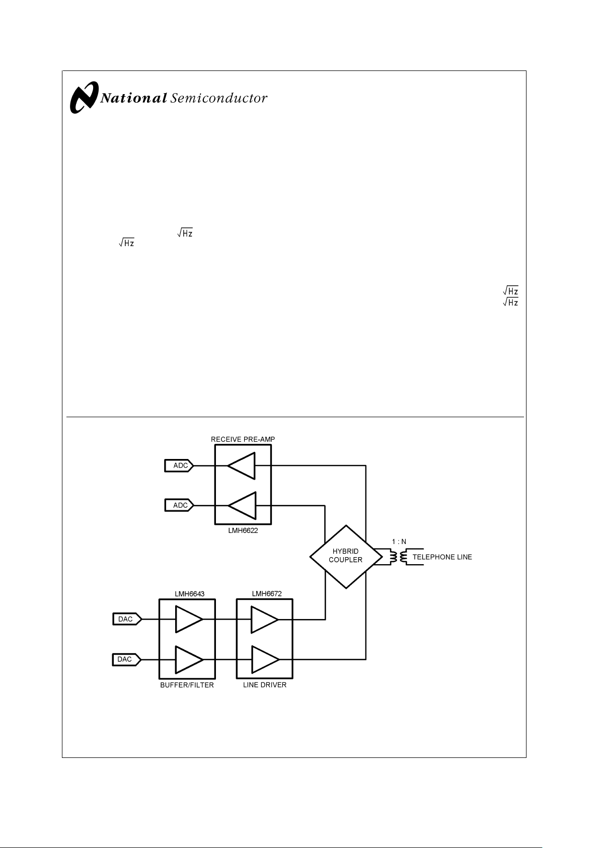
the LMH6622 an ideal choice for the receive channel amplifier in ADSL, VDSL, or other xDSL designs. The LMH6622
operates from
±
2.5V to±6V in dual supply mode and from
+5V to +12V in single supply configuration. The LMH6622 is
stable for A
V
≥ 2orAV≤−1. The fabrication of the LMH6622
on National Semiconductor’s advanced VIP10 process enables excellent (160MHz) bandwidth at a current consumption of only 4.3mA/amplifier. Packages for this dual amplifier
are the 8-lead SOIC and the 8-lead MSOP.
Features
VS=±6V, TA= 25˚C, Typical values unless specified
n Bandwidth (A
V
= +2) 160MHz
n Supply Voltage Range
±
2.5V to±6V +5V to +12
n Slew rate 85V/µs
n Supply current 4.3mA/amp
n Input common mode voltage −4.75V to +5.7V
n Output Voltage Swing (R
L
= 100Ω)
±
4.6V
n Input voltage noise 1.6nV/
n Input current noise 1.5pA/
n Linear output current 90mA
n Excellent harmonic distortion 90dBc
Applications
n xDSL receiver
n Low noise instrumentation front end
n Ultrasound preamp
n Active filters
n Cellphone basestation
20029226
xDSL Analog Front End
February 2002
LMH6622 Dual Wideband, Low Noise, 160MHz, Operational Amplifiers
© 2002 National Semiconductor Corporation DS200292 www.national.com
Page 2
Absolute Maximum Ratings (Note 1)
If Military/Aerospace specified devices are required,
please contact the National Semiconductor Sales Office/
Distributors for availability and specifications.
ESD Tolerance
Human Body Model 2kV (Note 2)
Machine Model 200V (Note 2)
V
IN
Differential
±
1.2V
Supply Voltage (V
+–V−
) 13.2V
Voltage at Input Pins V
+
+0.5V, V−−0.5V
Soldering Information
Infrared or Convection (20 sec) 235˚C
Wave Soldering (10 sec) 260˚C
Storage Temperature Range −65˚C to +150˚C
Junction Temperature (Note 4) +150˚C
Operating Ratings (Note 1)
Supply Voltage (V
+–V−
)
±
2.25V to±6V
Junction Temperature Range
(Note 3), (Note 4)
−40˚C to +85˚C
Package Thermal Resistance (Note 4) (θ
JA
)
8-pin SOIC 166˚C/W
8-pin MSOP 211˚C/W
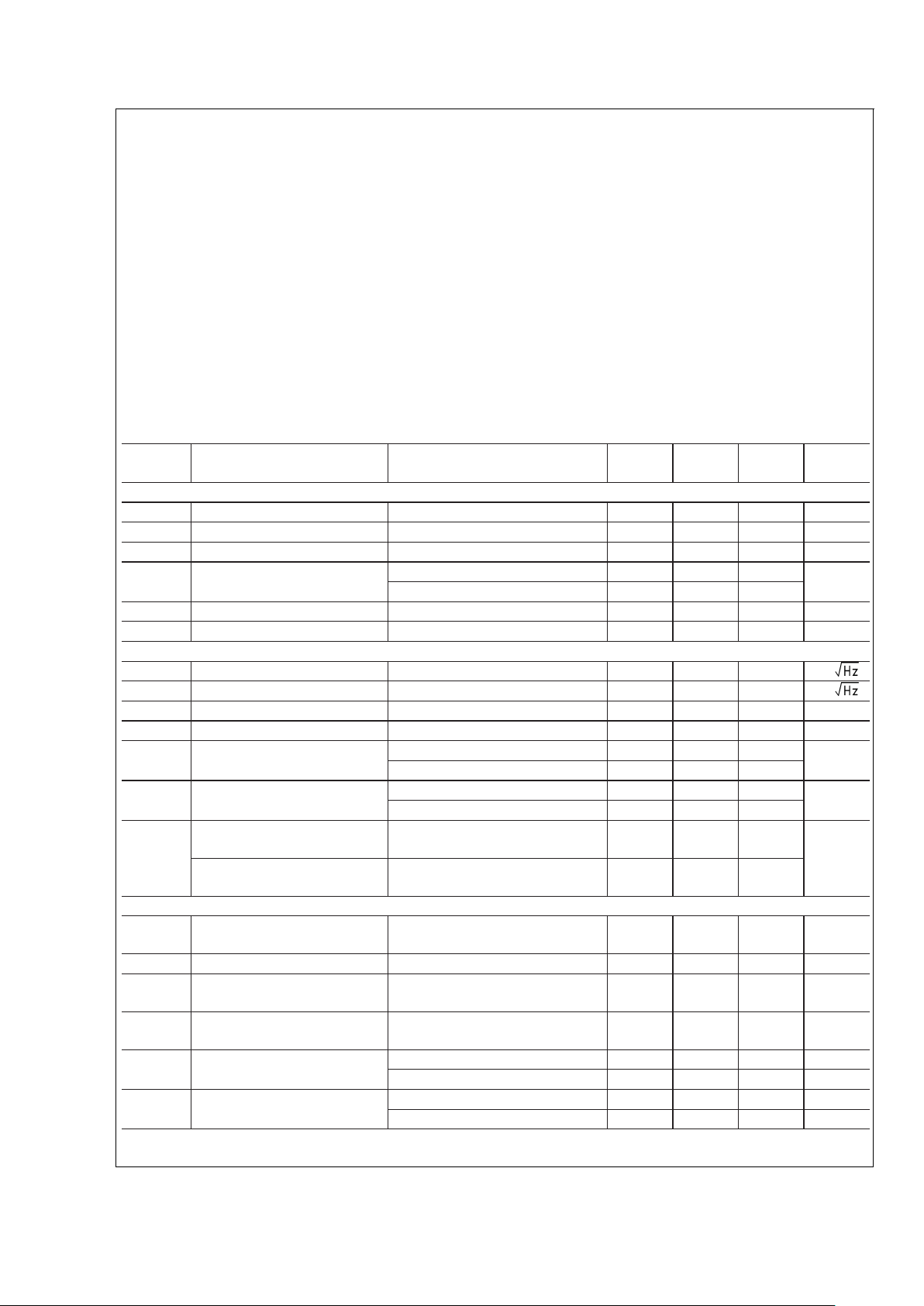
±
6V Electrical Characteristics
Unless otherwise specified, TJ= 25˚C, V+= 6V, V−= −6V, VCM= 0V, AV= +2, RF= 500Ω,RL= 100Ω. Boldface limits apply
at the temperature extremes.
Symbol Parameter Conditions Min
(Note 6)
Typ
(Note 5)
Max
(Note 6)
Units
Dynamic Performance
f
CL
−3dB BW VO= 200mV
PP
160 MHz
BW
0.1dB
0.1dB Gain Flatness VO= 200mV
PP
30 MHz
SR Slew Rate (Note 8) V
O
=2V
PP
85 V/µs
TS Settling Time V
O
=2VPPto±0.1% 40
ns
V
O
=2VPPto±1.0% 35
Tr Rise Time V
O
= 0.2V Step, 10% to 90% 2.3 ns
Tf Fall Time V
O
= 0.2V Step, 10% to 90% 2.3 ns
Distortion and Noise Response
e
n
Input Referred Voltage Noise f = 100kHz 1.6 nV/
i
n
Input Referred Current Noise f = 100kHz 1.5 pA/
DG Differential Gain RL= 150Ω,RF= 470Ω, NTSC 0.03 %
DP Differential Phase R
L
= 150Ω,RF= 470Ω, NTSC 0.03 deg
HD2 2
nd
Harmonic Distortion fc= 1MHz, VO=2VPP,RL= 100Ω −90
dBc
f
c
= 1MHz, VO=2VPP,RL= 500Ω −100
HD3 3
rd
Harmonic Distortion fc= 1MHz, VO=2VPP,RL= 100Ω −94
dBc
f
c
= 1MHz, VO=2VPP,RL= 500Ω −100
MTPR Upstream V
O
= 0.6 V
RMS
, 26kHz to 132kHz
(see test circuit 5)
−78
dBc
Downstream V
O
= 0.6 V
RMS
, 144kHz to 1.1MHz
(see test circuit 5)
−70
Input Characteristics
V
OS
Input Offset Voltage VCM= 0V −1.2
−2
+0.2 +1.2
+2
mV
TC V
OS
Input Offset Average Drift VCM= 0V (Note 7) −2.5 µV/˚C
I
OS
Input Offset Current VCM=0V −1
−1.5
−0.04 1
1.5
µA
I
B
Input Bias Current VCM= 0V 4.7 10
15
µA
R
IN
Input Resistance Common Mode 17 MΩ
Differential Mode 12 kΩ
C
IN
Input Capacitance Common Mode 0.9 pF
Differential Mode 1.0 pF
LMH6622
www.national.com 2
Page 3
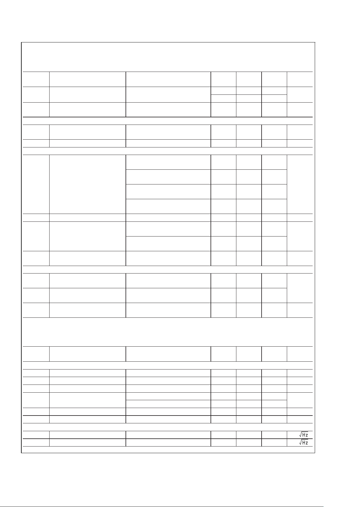
±
6V Electrical Characteristics (Continued)
Unless otherwise specified, TJ= 25˚C, V+= 6V, V−= −6V, VCM= 0V, AV= +2, RF= 500Ω,RL= 100Ω. Boldface limits apply
at the temperature extremes.
Symbol Parameter Conditions Min
(Note 6)
Typ
(Note 5)
Max
(Note 6)
Units
CMVR Input Common Mode Voltage
Range
CMRR ≥ 60dB −4.75 −4.5
V
5.5 +5.7
CMRR Common-Mode Rejection Ratio Input Referred,
V
CM
= −4.2 to +5.2V
80
75
100 dB
Transfer Characteristics
A
VOL
Large Signal Voltage Gain VO=4V
PP
74
70
83 dB
X
t
Crosstalk f = 1MHz −75 dB
Output Characteristics
V
O
Output Swing No Load, Positive Swing 4.8
4.6
5.2
V
No Load, Negative Swing −5.0 −4.6
−4.4
R
L
= 100Ω, Positive Swing 4.0
3.8
4.6
R
L
= 100Ω, Negative Swing −4.6 −4
−3.8
R
O
Output Impedance f = 1MHz 0.08 Ω
I
SC
Output Short Circuit Current Sourcing to Ground
∆V
IN
= 200mV (Note 3), (Note 9)
100 135
mA
Sinking to Ground
∆V
IN
= −200mV (Note 3), (Note 9)
100 130
I
OUT
Output Current Sourcing, VO= +4.3V
Sinking, V
O
= −4.3V
90 mA
Power Supply
+PSRR Positive Power Supply
Rejection Ratio
Input Referred,
V
S
= +5V to +6V
80
74
95
dB
−PSRR Negative Power Supply
Rejection Ratio
Input Referred,
V
S
= −5V to −6V
75
69
90
I
S
Supply Current (per amplifier) No Load 4.3 6
6.5
mA
±
2.5V Electrical Characteristics
Unless otherwise specified, all limits guaranteed for TJ= 25˚C, V+= 2.5V, V−= −2.5V, VCM= 0V, AV= +2, RF= 500Ω,
R
L
= 100Ω. Boldface limits apply at the temperature extremes.
Symbol Parameter Conditions Min
(Note 6)
Typ
(Note 5)
Max
(Note 6)
Units
Dynamic Performance
f
CL
−3dB BW VO= 200mV
PP
150 MHz
BW
0.1dB
0.1dB Gain Flatness VO= 200mV
PP
20 MHz
SR Slew Rate (Note 8) V
O
=2V
PP
80 V/µs
T
S
Settling Time VO=2VPPto±0.1% 45
ns
V
O
=2VPPto±1.0% 40
T
r
Rise Time VO= 0.2V Step, 10% to 90% 2.5 ns
T
f
Fall Time VO= 0.2V Step, 10% to 90% 2.5 ns
Distortion and Noise Response
e
n
Input Referred Voltage Noise f = 100kHz 1.7 nV/
i
n
Input Referred Current Noise f = 100kHz 1.5 pA/
LMH6622
www.national.com3
Page 4
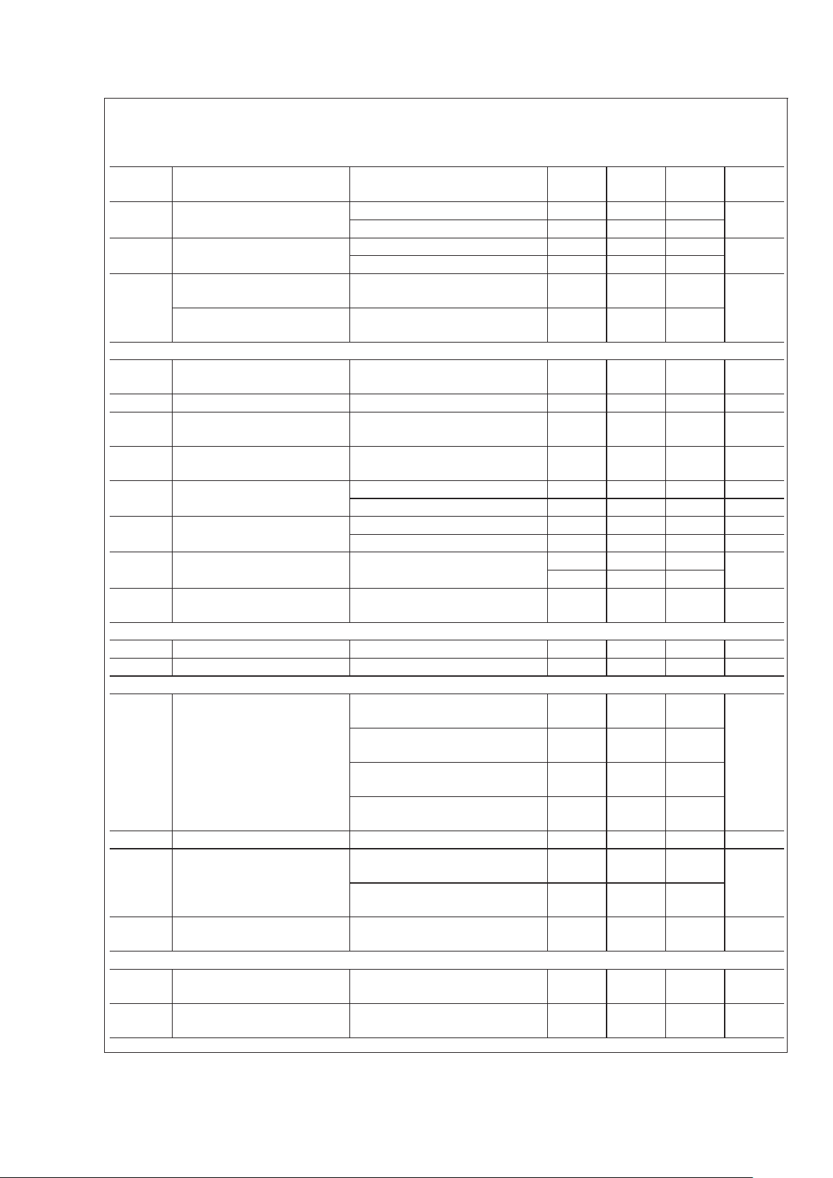
±
2.5V Electrical Characteristics (Continued)
Unless otherwise specified, all limits guaranteed for TJ= 25˚C, V+= 2.5V, V−= −2.5V, VCM= 0V, AV= +2, RF= 500Ω,
R
L
= 100Ω. Boldface limits apply at the temperature extremes.
Symbol Parameter Conditions Min
(Note 6)
Typ
(Note 5)
Max
(Note 6)
Units
HD2 2
nd
Harmonic Distortion fc = 1MHz, VO=2VPP,RL= 100Ω −88
dBc
fc = 1MHz, V
O
=2VPP,RL= 500Ω −98
HD3 3
rd
Harmonic Distortion fc = 1MHz, VO=2VPP,RL= 100Ω −92
dBc
fc = 1MHz, V
O
=2VPP,RL= 500Ω −100
MTPR Upstream V
O
= 0.4V
RMS
,26kHz to 132kHz
(see test circuit 5)
−76
dBc
Downstream V
O
= 0.4V
RMS
,144kHz to 1.1MHz
(see test circuit 5)
−68
Input Characteristics
V
OS
Input Offset Voltage VCM= 0V −1.5
−2.3
+0.3 +1.5
+2.3
mV
TC V
OS
Input Offset Average Drift VCM= 0V (Note 7) −2.5 µV/˚C
I
OS
Input Offset Current VCM= 0V −1.5
−2.5
+0.01 1.5
2.5
µA
I
B
Input Bias Current VCM= 0V 4.6 10
15
µA
R
IN
Input Resistance Common Mode 17 MΩ
Differential Mode 12 kΩ
C
IN
Input Capacitance Common Mode 0.9 pF
Differential Mode 1.0 pF
CMVR Input Common Mode Voltage
Range
CMRR ≥ 60dB −1.25 −1
V
2 +2.2
CMRR Common Mode Rejection Ratio Input Referred,
V
CM
= −0.7 to +1.7V
80
75
100 dB
Transfer Characteristics
A
VOL
Large Signal Voltage Gain VO=1V
PP
74 82 dB
X
t
Crosstalk f = 1MHz −75 dB
Output Characteristics
V
O
Output Swing No Load, Positive Swing 1.4
1.2
1.7
V
No Load, Negative Swing −1.5 −1.2
−1
R
L
= 100Ω, Positive Swing 1.2
1
1.5
R
L
= 100Ω, Negative Swing −1.4 −1.1
−0.9
R
O
Output Impedance f = 1MHz 0.1 Ω
I
SC
Output Short Circuit Current Sourcing to Ground
∆V
IN
= 200mV (Note 3), (Note 9)
100 137
mA
Sinking to Ground
∆V
IN
= −200mV (Note 3), (Note 9)
100 134
I
OUT
Output Current Sourcing, VO= +0.8V
Sinking, V
O
= −0.8V
90 mA
Power Supply
+PSRR Positive Power Supply Rejection
Ratio
Input Referred,
V
S
= +2.5V to +3V
78
72
93
dB
−PSRR Negative Power Supply
Rejection Ratio
Input Referred,
V
S
= −2.5V to −3V
75
70
88 dB
LMH6622
www.national.com 4
Page 5

±
2.5V Electrical Characteristics (Continued)
Unless otherwise specified, all limits guaranteed for TJ= 25˚C, V+= 2.5V, V−= −2.5V, VCM= 0V, AV= +2, RF= 500Ω,
R
L
= 100Ω. Boldface limits apply at the temperature extremes.
Symbol Parameter Conditions Min
(Note 6)
Typ
(Note 5)
Max
(Note 6)
Units
I
S
Supply Current (per amplifier) No Load 4.1 5.8
6.4
mA
Note 1: Absolute Maximum Ratings indicate limits beyond which damage to the device may occur. Operating Ratings indicate conditions for which the device is
intended to be functional, but specific performance is not guaranteed. For guaranteed specifications and the test conditions, see the Electrical Characteristics.
Note 2: Human body model, 1.5kΩ in series with 100pF. Machine model, 0Ω in series with 200pF.
Note 3: Applies to both single-supply and split-supply operation. Continuous short circuit operation at elevated ambient temperature can result in exceeding the
maximum allowed junction temperature of 150˚C.
Note 4: The maximum power dissipation is a function of T
J(MAX)
, θJAand TA. The maximum allowable power dissipation at any ambient temperature is PD=
(T
J(MAX)−TA
)/θJA. All numbers apply for packages soldered directly onto a PC board.
Note 5: Typical values represent the most likely parametric norm.
Note 6: All limits are guaranteed by testing or statistical analysis.
Note 7: Offset voltage average drift is determined by dividing the change in V
OS
at temperature extremes into the total temperature change.
Note 8: Slew rate is the slowest of the rising and falling slew rates.
Note 9: Short circuit test is a momentary test.Output short circuitduration is infinitefor V
S
≤±2.5V,atroom temperature andbelow.For V
S
>
±
2.5V,allowableshort
circuit duration is 1.5ms.
LMH6622
www.national.com5
Page 6
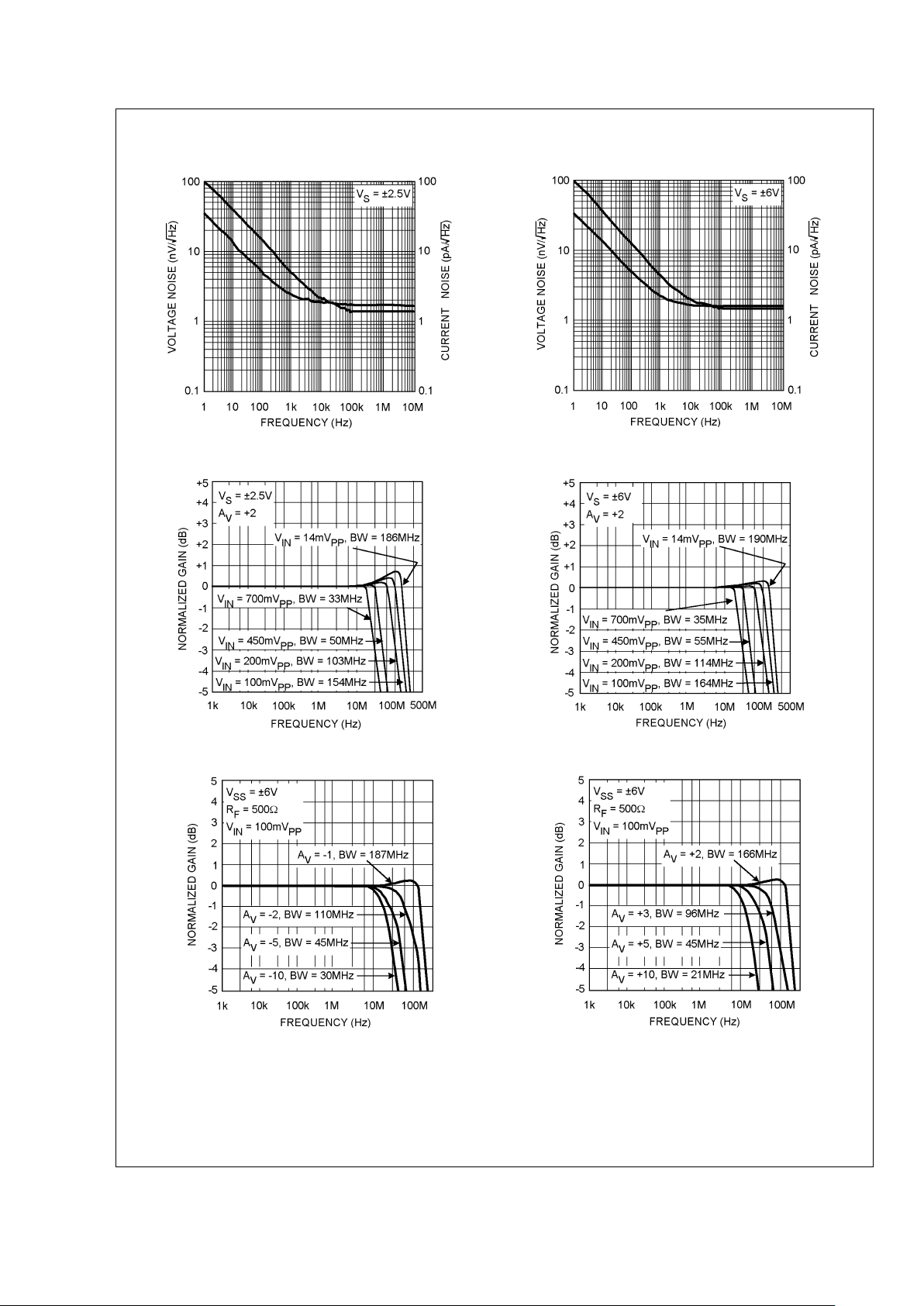
Typical Performance Characteristics
Current and Voltage Noise vs. Frequency Current and Voltage Noise vs. Frequency
20029224
20029225
Frequency Response vs. Input Signal Level Frequency Response vs. Input Signal Level
20029202 20029203
Inverting Amplifier Frequency Response Non-Inverting Amplifier Frequency Response
20029246 20029247
LMH6622
www.national.com 6
Page 7

Typical Performance Characteristics (Continued)
Open Loop Gain and Phase Response Crosstalk vs. Frequency
20029205
20029201
PSRR vs. Frequency CMRR vs. Frequency
20029204
20029206
Positive Output Swing vs. Source Current Negative Output Swing vs. Sink Current
20029248 20029249
LMH6622
www.national.com7
Page 8

Typical Performance Characteristics (Continued)
Non-Inverting Small Signal Pulse Response
V
S
=±2.5V, RL= 100Ω,AV= +2, RF= 500Ω
Non-Inverting Small Signal Pulse Response
VS=±6V, RL= 100Ω,AV= +2, RF= 500Ω
20029207 20029209
Non-Inverting Large Signal Pulse Response
V
S
=±2.5V, RL= 100Ω,AV= +2, RF= 500Ω
Non-Inverting Large Signal Pulse Response
VS=±6V, RL= 100Ω,AV= +2, RF= 500Ω
20029208 20029210
Harmonic Distortion vs. Input Signal Level Harmonic Distortion vs. Input Signal Level
20029212 20029213
LMH6622
www.national.com 8
Page 9

Typical Performance Characteristics (Continued)
Harmonic Distortion vs. Frequency Harmonic Distortion vs. Frequency
20029214 20029215
Harmonic Distortion vs. Input Signal Level Harmonic Distortion vs. input Signal Level
20029216 20029217
Harmonic Distortion vs. Input Frequency Harmonic Distortion vs. Input Frequency
20029218 20029219
LMH6622
www.national.com9
Page 10

Typical Performance Characteristics (Continued)
Full Rate ADSL (DMT) Upstream MTPR
@
VS=±2.5V Full Rate ADSL (DMT) Downstream MTPR@VS=±2.5V
20029256 20029258
Full Rate ADSL (DMT) Upstream MTPR@VS=±6V Full Rate ADSL (DMT) Downstream MTPR@VS=±6V
20029257 20029259
LMH6622
www.national.com 10
Page 11

Connection Diagram
8-Pin SOIC/MSOP
20029211
Top View
Ordering Information
Package Part Number Package Marking Transport Media NSC Drawing
8-Pin SOIC LMH6622MA LMH6622MA 95 Units per Rail M08A
LMH6622MAX 2.5k Units Tape and Reel
8-Pin MSOP LMH6622MM A80A 1k Units Tape and Reel MUA08A
LMH6622MMX 3.5k Units Tape and Reel
Test Circuits
20029250
1) Non-Inverting Amplifier
20029251
2) CMRR
20029253
3) Voltage Noise
R
G
=1Ωfor f ≤ 100kHz, RG=20Ωfor f>100kHz
20029252
4) Current Noise
R
G
=1Ωfor f ≤ 100kHz, RG=20Ωfor f>100kHz
LMH6622
www.national.com11
Page 12

Test Circuits (Continued)
20029255
5) Multitone Power Ratio, RF= 500Ω,RG= 174Ω,RL=
437Ω
DSL Receive Channel Applications
The LMH6622 is a dual, wideband operational amplifier designed for use as a DSL line receiver. In the receive band of
a Customer Premises Equipment (CPE) ADSL modem it is
possible that as many as 255 Discrete Multi-Tone (DMT)
QAM signals will be present, each with its own carrier frequency, modulation, and signal level. The ADSL standard
requires a line referred noise power density of -140dBm/Hz
within theCPE receive bandof 100KHz to 1.1MHz. The CPE
driver output signal will leak into the receive path because of
full duplex operation and the imperfections of the hybrid
coupler circuit. The DSL analog front end must incorporate a
receiver pre-amp which is both low noise and highly linear
for ADSL-standard operation. The LMH6622 is designed for
the twin performance parameters of low noise and high
linearity.
Applications ranging from +5V to +12V or
±
2.5V to±6V are
fully supportedby the LMH6622. In
Figure 2
, theLMH6622 is
used as an inverting summing amplifier to provide both
received pre-amp channel gain and driver output signal cancellation, i.e., the function of a hybrid coupler.
20029223
FIGURE 1. ADSL Signal Description
LMH6622
www.national.com 12
Page 13

DSL Receive Channel Applications (Continued)
20029227
FIGURE 2. ADSL Receive Applications Circuit
LMH6622
www.national.com13
Page 14

DSL Receive Channel Applications
(Continued)
The two R
S
resistors are used to provide impedance match-
ing through the 1:N transformer.
Where RLis the impedance of the twisted pair line.
N is the turns ratio of the transformer.
The resistors R
2
and RFare used to set the receive gain of
the pre-amp. The receive gain is selected to meet the ADC
full-scale requirement of a DSL chipset.
Resistor R
1
and R2along with RFare used to achieve
cancellation of the output driver signal at the output of the
receiver.
Since the LMH6622 is configured as an inverting summing
amplifier, V
OUT
is found to be,
The expression for V1and V2can be found by using superposition principle.
When V
S
=0,
When VA=0,
Therefore,
And then,
Setting R1= 2*R2to cancel unwanted driver signal in the
receive path, then we have
We can also find that,
And then
In conclusion, the peak-to-peak voltage to the ADC would
be,
Receive Channel Noise Calculation
The circuit of
Figure 2
also has the characteristic that it
cancels noise power from the drive channel.
The noise gain of the receive pre-amp is found to be:
Noise power at each of the output of LMH6622:
where
V
n
Input referred voltage noise
i
n
Input referred current noise
i
non-inv
Input referred non-inverting current noise
i
inv
Input referred inverting current noise
k Boltzmann’s constant, K = 1.38 x 10
−23
T Resistor temperature in k
R
+
Source resistance at the non-inverting input
to balance offset voltage, typically very small
for this inverting summing applications
For a voltage feedback amplifier,
Therefore, total output noise from the differential pre-amp is:
The factor ’2 ’ appears here because of differential output.
Differential Analog-to-Digital Driver
20029239
FIGURE 3. Circuit for Differential A/D Driver
LMH6622
www.national.com 14
Page 15

DSL Receive Channel Applications
(Continued)
The LMH6622 is a low noise, low distortion high speed
operational amplifier. The LMH6622 comes in either SOIC-8
or MSOP-8 packages. Because two channels are available
in each package the LMH6622 can be used as a high
dynamic rangedifferential amplifier for the purpose of driving
a high speed analog-to-digital converter.Driving a 1kΩ load,
the differentialamplifier of
Figure 3
provides 20dBgain, a flat
frequency response up to 6MHz, and harmonic distortion
that is lower than 80dBc. This circuit makes use of a transformer to convert a single-ended signal to a differential signal. The input resistor R
IN
is chosen by the following equa-
tion,
The gain of this differential amplifier can be adjusted by R
C
and RF,
20029221
FIGURE 4. Frequency Response
20029222
FIGURE 5. Total Output Referred Noise Density
LMH6622
www.national.com15
Page 16

DSL Receive Channel Applications
(Continued)
Circuit Layout Considerations
National Semiconductorsuggests the copperpatterns on the
evaluation boards listed below as a guide for high frequency
layout. These boards are also useful as an aid in device
testing and characterization. As is the case with all highspeed amplifiers, accepted-practice R
F
design technique on
the PCB layout is mandatory. Generally, a good high frequency layout exhibits a separation of power supply and
ground traces from theinverting input and output pins. Parasitic capacitances between these nodes and ground will
cause frequency response peaking and possible circuit oscillations (see Application Note OA-15 for more information).
High quality chip capacitors with values in the range of
1000pF to 0.1µF should be used for power supply bypassing. One terminal of each chip capacitor is connected to the
ground plane and the other terminal is connected to a point
that is as close as possible to each supply pin as allowed by
the manufacturer’s design rules. In addition, a tantalum capacitor with a value between 4.7µF and 10µF should be
connected in parallel with the chip capacitor. Signal lines
connecting the feedback and gain resistors should be as
short as possible to minimize inductance and microstrip line
effect. Input and output termination resistors should be
placed as close as possible to the input/output pins. Traces
greater than 1 inch in length should be impedance matched
to the corresponding load termination.
Symmetry between the positive and negative paths in the
layout of differential circuitry should be maintained so as to
minimize the imbalance of amplitude and phase of the differential signal.
Device Package Evaluation Board P/N
LMH6622MA SOIC-8 CLC730036
LMH6622MM MSOP-8 CLC730123
These free evaluation boards are shipped when a device
sample request is placed with National Semiconductor.
Component value selection is another important parameter
in working with high speed/high performance amplifiers.
Choosing external resistorsthat are large in value compared
to thevalue of other criticalcomponents will affectthe closed
loop behavior of the stage because of the interaction of
these resistors with parasitic capacitances. These parasitic
capacitors could either be inherent to the device or be a
by-product of the board layout and component placement.
Moreover,a large resistor will alsoadd more thermalnoise to
the signal path. Either way, keeping the resistor values low
will diminish this interaction. On the other hand, choosing
very low value resistors could load down nodes and will
contribute to higher overall power dissipation and worse
distortion.
Driving Capacitive Load
Capacitive Loads decrease the phase marginof all op amps.
The output impedance of a feedback amplifier becomes
inductive at high frequencies, creating a resonant circuit
when the load is capacitive. This can lead to overshoot,
ringing and oscillation. To eliminate oscillation or reduce
ringing, an isolation resistor can be placed between the load
and the output. In general, the bigger the isolation resistor,
the more damped the pulse response becomes. For initial
evaluation, a 50Ω isolation resistor is recommended.
LMH6622
www.national.com 16
Page 17

Physical Dimensions inches (millimeters)
unless otherwise noted
8-Pin SOIC
NS Package Number M08A
8-Pin MSOP
NS Package Number MUA08A
LMH6622
www.national.com17
Page 18

Notes
LIFE SUPPORT POLICY
NATIONAL’S PRODUCTS ARE NOT AUTHORIZED FOR USE AS CRITICAL COMPONENTS IN LIFE SUPPORT
DEVICES OR SYSTEMS WITHOUT THE EXPRESS WRITTEN APPROVAL OF THE PRESIDENT AND GENERAL
COUNSEL OF NATIONAL SEMICONDUCTOR CORPORATION. As used herein:
1. Life support devices or systems are devices or
systems which, (a) are intended for surgical implant
into the body, or (b) support or sustain life, and
whose failure to perform when properly used in
accordance with instructions for use provided in the
labeling, can be reasonably expected to result in a
significant injury to the user.
2. A critical component is any component of a life
support device or system whose failure to perform
can be reasonably expected to cause the failure of
the life support device or system, or to affect its
safety or effectiveness.
National Semiconductor
Corporation
Americas
Email: support@nsc.com
National Semiconductor
Europe
Fax: +49 (0) 180-530 85 86
Email: europe.support@nsc.com
Deutsch Tel: +49 (0) 69 9508 6208
English Tel: +44 (0) 870 24 0 2171
Français Tel: +33 (0) 1 41 91 8790
National Semiconductor
Asia Pacific Customer
Response Group
Tel: 65-2544466
Fax: 65-2504466
Email: ap.support@nsc.com
National Semiconductor
Japan Ltd.
Tel: 81-3-5639-7560
Fax: 81-3-5639-7507
www.national.com
LMH6622 Dual Wideband, Low Noise, 160MHz, Operational Amplifiers
National does not assume any responsibility for use of any circuitry described, no circuit patent licenses are implied and National reserves the right at any time without notice to change said circuitry and specifications.
 Loading...