

Page 1
April 2007
LMH6552
1 GHz Fully Differential Amplifier
General Description
The LMH6552 is a high performance fully differential amplifier
designed to provide the exceptional signal fidelity and wide
large-signal bandwidth necessary for driving 8 to 14 bit high
speed data acquisition systems. Using National's proprietary
differential current mode input stage architecture, the
LMH6552 allows operation at gains greater than unity without
sacrificing response flatness, bandwidth, harmonic distortion,
or output noise performance.
With external gain set resistors and integrated common mode
feedback, the LMH6552 can be configured as either a differential input to differential output or single ended input to
differential output gain block. The LMH6552 can be AC or DC
coupled at the input which makes it suitable for a wide range
of applications including communication systems and high
speed oscilloscope front ends. The LMH6552 is available in
an 8-pin SOIC package as well as a space saving, thermally
enhanced 8-pin LLP package for higher performance.
Features
■
1.0 GHz bandwidth @ AV = 1
■
800 MHz bandwidth @ AV = 4
■
450 MHz 0.1 dB flatness
■
3800 V/µs slew rate
■
10 ns settling time to 0.1%
■
−90 dB THD @ 20 MHz
■
−74 dB THD @ 70 MHz
■
20 ns enable/shutdown pin
■
5 to 12V operation
Applications
■
Differential ADC driver
■
Video over twisted pair
■
Differential line driver
■
Single end to differential converter
■
High speed differential signaling
■
IF/RF amplifier
■
SAW filter buffer/driver
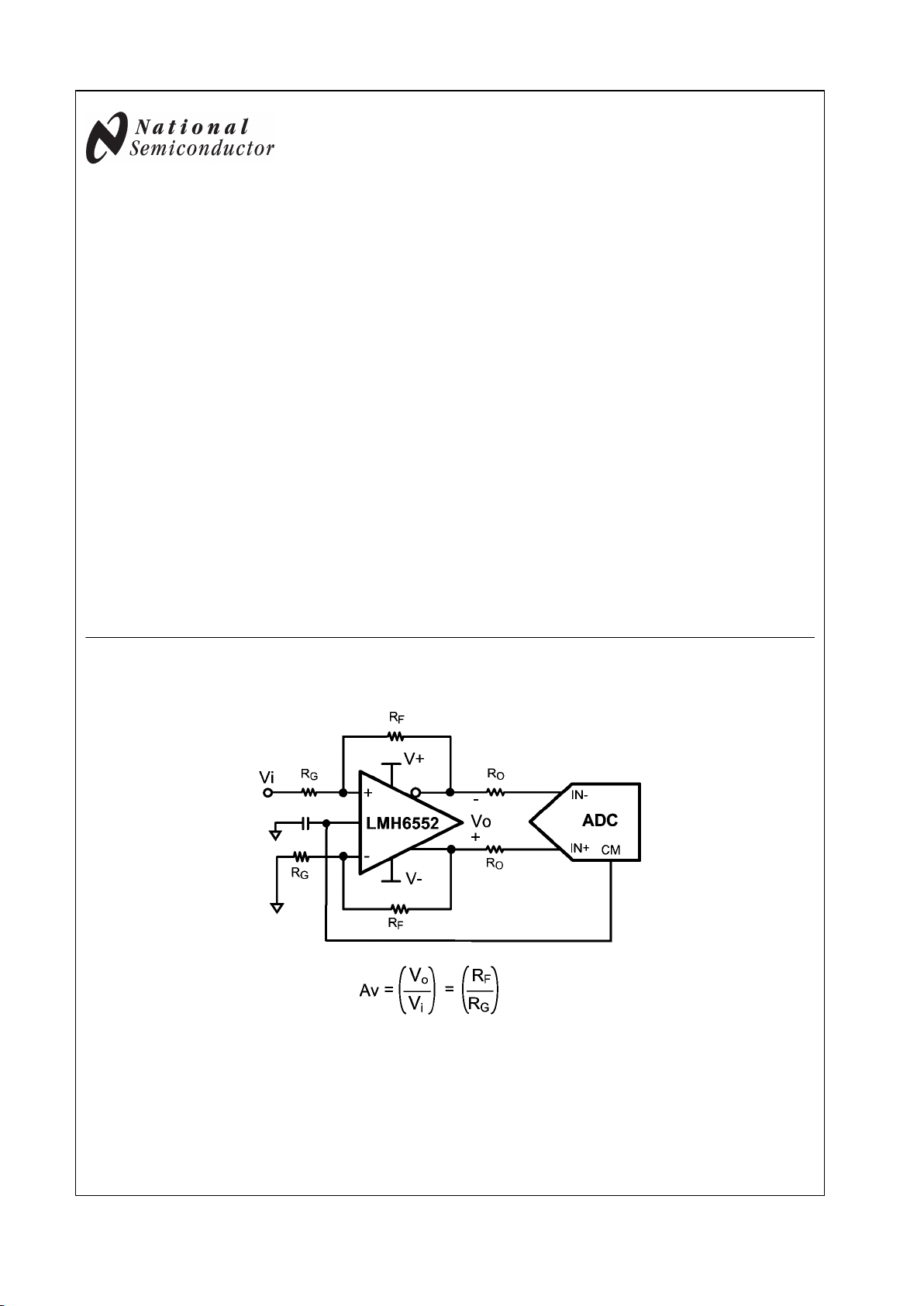
Typical Application
Single-Ended Input Differential Output
30003544
LMH™ is a trademark of National Semiconductor Corporation.
© 2007 National Semiconductor Corporation 300035 www.national.com
LMH6552 1 GHz Fully Differential Amplifier
Page 2
Absolute Maximum Ratings (Note 1)
If Military/Aerospace specified devices are required,
please contact the National Semiconductor Sales Office/
Distributors for availability and specifications.
ESD Tolerance (Note 6)
Human Body Model 2000V
Machine Model 200V
Supply Voltage 13.2V
Common Mode Input Voltage ±V
S
Maximum Input Current (pins 1, 2, 7, 8) 30 mA
Maximum Output Current (pins 4, 5) (Note 4)
Soldering Information
Infrared or Convection (20 sec) 235°C
Wave Soldering (10 sec) 260°C
Operating Ratings (Note 1)
Operating Temperature Range
(Note 3) −40°C to +85°C
Storage Temperature Range −65°C to +150°C
Total Supply Voltage 4.5V to 12V
Package Thermal Resistance (θJA) (Note 5)
8-Pin SOIC 150°C/W
±5V Electrical Characteristics (Note 2)
Unless otherwise specified, all limits are guaranteed for TA = 25°C, V+ = +5V, V− = −5V, AV= 1, VCM = 0V, RF = RG = 357Ω,
RL = 500Ω, for single ended in, differential out. Boldface limits apply at the temperature extremes.
Symbol Parameter Conditions Min
(Note 8)
Typ
(Note 7)
Max
(Note 8)
Units
AC Performance (Differential)
SSBW Small Signal −3 dB Bandwidth
(Note 8)
V
OUT
= 0.2 VPP, AV = 1 1000
MHz
V
OUT
= 0.2 VPP, AV = 2 930
V
OUT
= 0.2 VPP, AV = 4 810
V
OUT
= 0.2 VPP, AV = 8 590
LSBW Large Signal −3 dB Bandwidth V
OUT
= 2 VPP, AV = 1 950
MHz
V
OUT
= 2 VPP, AV = 2 820
V
OUT
= 2 VPP, AV = 4 740
V
OUT
= 2 VPP, AV = 8 590
0.1 dB Bandwidth V
OUT
= 0.2 VPP, AV = 1 450 MHz
Slew Rate 4V Step, AV = 1 3800
V/μs
Rise/Fall Time, 10%-90% 2V Step 750 ps
0.1% Settling Time 2V Step 10 ns
Distortion and Noise Response
HD2 2nd Harmonic Distortion
V
OUT
= 2 VPP, f = 20 MHz, RL = 800Ω
−92
dBc
V
OUT
= 2 VPP, f = 70 MHz, RL = 800Ω
−74
HD3 3rd Harmonic Distortion
V
OUT
= 2 VPP, f = 20 MHz, RL = 800Ω
−93
dBc
V
OUT
= 2 VPP, f = 70 MHz, RL = 800Ω
−84
IMD3 Two-Tone Intermodulation Freq >70 MHz, Third Order Products,
V
OUT
= 2 VPP Composite
−87 dBc
Input Noise Voltage
f ≥ 1 MHz
1.1
nV/
Input Noise Current
f ≥ 1 MHz
19.5
pA/
Noise Figure (See Figure 5)
50Ω System, AV = 9, 10 MHz
10.3 dB
Input Characteristics
I
BI
Input Bias Current (Note 10) 60 110 µA
I
Boffset
Input Bias Current Differential
(Note 7)
VCM = 0V, VID = 0V, I
Boffset
= (I
B
−
- I
B
+
)/2 2.47 18 µA
CMRR Common Mode Rejection Ratio
(Note 7)
DC, VCM = 0V, VID = 0V 80 dBc
R
IN
Input Resistance Differential 15
Ω
C
IN
Input Capacitance Differential 0.5 pF
CMVR Input Common Mode Voltage
Range
CMRR > 38 dB ±3.5 ±3.8 V
www.national.com 2
LMH6552
Page 3
Symbol Parameter Conditions Min
(Note 8)
Typ
(Note 7)
Max
(Note 8)
Units
Output Performance
Output Voltage Swing (Note 7) Differential Output 14.8 15.4 V
PP
I
OUT
Linear Output Current (Note 7) V
OUT
= 0V ±70 ±80 mA
I
SC
Short Circuit Current One Output Shorted to Ground VIN = 2V
Single Ended (Note 6)
±141 mA
Output Balance Error
ΔV
OUT
Common Mode /ΔV
OUT
Differential , ΔVOD = 1V, f < 1 MHz
-60 dB
Miscellaneous Performance
Z
T
Open Loop Transimpedance Differential 108
dBΩ
PSRR Power Supply Rejection Ratio
DC, ΔVS = ±1V
80 dB
I
S
Supply Current (Note 7)
RL = ∞
19 22.5 25
28
mA
Enable Voltage Threshold 3.0 V
Disable Voltage Threshold 2.0 V
Enable/Disable time 15 ns
I
SD
Disable Shutdown Current 500 600
μA
Output Common Mode Control Circuit
Common Mode Small Signal
Bandwidth
V
IN
+
= V
IN
−
= 0 400 MHz
Slew Rate V
IN
+
= V
IN
−
= 0 607
V/μs
V
OSCM
Input Offset Voltage Common Mode, VID = 0, VCM = 0 1.5 ±16.5 mV
Input Bias Current (Note 9) −3.2 ±8 µA
Voltage Range ±3.7 ±3.8 V
CMRR Measure VOD, VID = 0V 80 dB
Input Resistance 200
kΩ
Gain
ΔV
O,CM
/ΔV
CM
0.995 1.0 1.012 V/V
±2.5V Electrical Characteristics (Note 2)
Unless otherwise specified, all limits are guaranteed for TA = 25°C, V+ = +2.5V, V− = −2.5V, AV = 1, VCM = 0V, RF = RG = 357Ω,
RL = 500Ω, for single ended in, differential out. Boldface limits apply at the temperature extremes.
Symbol Parameter Conditions Min
(Note 8)
Typ
(Note 7)
Max
(Note 8)
Units
SSBW Small Signal −3 dB Bandwidth
(Note 8)
V
OUT
= 0.2 VPP, AV = 1 800
MHz
V
OUT
= 0.2 VPP, AV = 2 740
V
OUT
= 0.2 VPP, AV = 4 660
V
OUT
= 0.2 VPP, AV = 8 498
LSBW Large Signal −3 dB Bandwidth V
OUT
= 2 VPP, AV = 1 690
MHz
V
OUT
= 2 VPP, AV = 2 620
V
OUT
= 2 VPP, AV = 4 589
V
OUT
= 2 VPP, AV = 8 480
0.1 dB Bandwidth V
OUT
= 0.2 VPP, AV = 1 300 MHz
Slew Rate 2V Step, AV = 1 2100
V/μs
Rise/Fall Time, 10% to 90% 2V Step 1.2 ns
0.1% Settling Time 2V Step 10 ns
Distortion and Noise Response
HD2 2nd Harmonic Distortion
V
OUT
= 2 VPP, f = 20 MHz, RL = 800Ω
82
dBc
V
OUT
= 2 VPP, f = 70 MHz, RL = 800Ω
65
3 www.national.com
LMH6552
Page 4
Symbol Parameter Conditions Min
(Note 8)
Typ
(Note 7)
Max
(Note 8)
Units
HD3 3rd Harmonic Distortion
V
OUT
= 2 VPP, f = 20 MHz, RL = 800Ω
79
dBc
V
OUT
= 2 VPP, f = 70 MHz, RL = 800Ω
67
IMD3 Two-Tone Intermodulation
f ≥ 70 MHz, Third Order Products,
V
OUT
= 2 VPP Composite
−77 dBc
Input Noise Voltage
f ≥ 1 MHz
1.1
nV/
Input Noise Current
f ≥ 1 MHz
19.5
pA/
Noise Figure (See Figure 5)
50Ω System, AV = 9, 10 MHz
10.2 dB
Input Characteristics
I
BI
Input Bias Current (Note 10) 54 90 µA
I
Boffset
Input Bias Current Differential
(Note 7)
VCM = 0V, VID = 0V, I
Boffset
= (I
B
−
- I
B
+
)/2 2.3 18
μA
CMRR Common-Mode Rejection Ratio
(Note 7)
DC, VCM = 0V, VID = 0V 75 dBc
R
IN
Input Resistance Differential 15
Ω
C
IN
Input Capacitance Differential 0.5 pF
CMVR Input Common Mode Range CMRR > 38 dB 1.5-3.5 1.2-3.8 V
Output Performance
Output Voltage Swing (Note 7) Differential Output 5.6 6.0 V
PP
I
OUT
Linear Output Current (Note 7) V
OUT
= 0V ±55 ±65 mA
I
SC
Short Circuit Current One Output Shorted to Ground, VIN = 2V
Single Ended (Note 6)
±131 mA
Output Balance Error
ΔV
OUT
Common Mode /ΔV
OUT
Differential , ΔVOD = 1V, f < 1 MHz
60 dB
Miscellaneous Performance
ZT Open Loop Transimpedance Differential 107
dBΩ
PSRR Power Supply Rejection Ratio
DC, ΔVS = ±1V
80 dB
I
S
Supply Current (Note 7)
RL = ∞
17 20.4 24
27
mA
Enable Voltage Threshold 3.0 V
Disable Voltage Threshold 2.0 V
Enable/Disable time 15 ns
I
SD
Disable Shutdown Current 500 600 µA
Output Common Mode Control Circuit
Common Mode Small Signal
Bandwidth
V
IN
+
= V
IN
−
= 0 310 MHz
Slew Rate V
IN
+
= V
IN
−
= 0 430
V/μs
V
OSCM
Input Offset Voltage Common Mode, VID = 0, VCM = 0 1.65 ±15 mV
Input Bias Current (Note 9) −2.9 µA
Voltage Range ±1.19 ±1.25 V
CMRR Measure VOD, VID = 0V 80 dB
Input Resistance 200
kΩ
Gain
ΔV
O,CM
/ΔV
CM
0.995 1.0 1.012 V/V
www.national.com 4
LMH6552
Page 5
Note 1: Absolute Maximum Ratings indicate limits beyond which damage to the device may occur. Operating Ratings indicate conditions for which the device is
intended to be functional, but specific performance is not guaranteed. For guaranteed specifications, see the Electrical Characteristics tables.
Note 2: Electrical Table values apply only for factory testing conditions at the temperature indicated. Factory testing conditions result in very limited self-heating
of the device such that TJ = TA. No guarantee of parametric performance is indicated in the electrical tables under conditions of internal self-heating where
TJ > TA. See Applications Section for information on temperature de-rating of this device." Min/Max ratings are based on product characterization and simulation.
Individual parameters are tested as noted.
Note 3: The maximum power dissipation is a function of T
J(MAX)
, θJA. The maximum allowable power dissipation at any ambient temperature is
PD = (T
J(MAX)
– TA) / θJA. All numbers apply for packages soldered directly onto a PC Board.
Note 4: The maximum output current (I
OUT
) is determined by device power dissipation limitations. See the Power Dissipation section of the Application Section
for more details.
Note 5: Human Body Model, applicable std. MIL-STD-883, Method 30157. Machine Model, applicable std. JESD22-A115-A (ESD MM std. of JEDEC). FieldInduced Charge-Device Model, applicable std. JESD22-C101-C (ESD FICDM std. of JEDEC).
Note 6: Short circuit current should be limited in duration to no more than 10 seconds. See the Power Dissipation section of the Application Information for more
details.
Note 7: Typical values represent the most likely parametric norm as determined at the time of characterization. Actual typical values may vary over time and will
also depend on the application and configuration. The typical values are not tested and are not guaranteed on shipped production material.
Note 8: Limits are 100% production tested at 25°C. Limits over the operating temperature range are guaranteed through correlation using Statistical Quality
Control (SQC) methods.
Note 9: Negative input current implies current flowing out of the device.
Note 10: IBI is referred to a differential output offset voltage by the following relationship: V
OD(offset)
= IBI*2R
F
Connection Diagram
8-Pin SOIC
30003508
Top View
Ordering Information
Package Part Number Package Marking Transport Media NSC Drawing
8-Pin SOIC
LMH6552MA
LMH6552MA
95/Rails
M08A
LMH6552MAX 2.5k Units Tape and Reel
5 www.national.com
LMH6552
Page 6
Typical Performance Characteristics V+ = +5V, V− = −5V (T
A
= 25°C, RF = RG =
357Ω, RL = 500Ω, AV = 1, for single ended in, differential out, unless specified).
Frequency Response vs. Gain
30003547
Frequency Response vs. Gain
30003534
Frequency Response vs. V
OUT
30003548
Frequency Response vs. V
OUT
30003516
Frequency Response vs. Supply Voltage
30003514
Frequency Response vs. Supply Voltage
30003515
www.national.com 6
LMH6552
Page 7

Frequency Response vs. Capacitive Load
30003521
Suggested R
OUT
vs. Capacitive Load
30003522
1 VPP Pulse Response Single Ended Input
30003526
2 VPP Pulse Response Single Ended Input
30003527
Large Signal Pulse Response
30003525
Output Common Mode Pulse Response
30003524
7 www.national.com
LMH6552
Page 8

Distortion vs. Frequency Single Ended Input
30003529
Distortion vs. Supply Voltage
30003543
Distortion vs. Supply Voltage
30003537
Distortion vs. Output Common Mode Voltage
30003538
Maximum V
OUT
vs. I
OUT
30003530
Minimum V
OUT
vs. I
OUT
30003531
www.national.com 8
LMH6552
Page 9

Open Loop Transimpedance
30003541
Open Loop Transimpedance
30003542
Closed Loop Output Impedance
30003517
Closed Loop Output Impedance
30003518
Overdrive Recovery
30003557
Overdrive Recovery
30003558
9 www.national.com
LMH6552
Page 10

PSRR
30003519
PSRR
30003520
CMRR
30003533
Balance Error
30003513
Noise Figure
30003545
Noise Figure
30003546
www.national.com 10
LMH6552
Page 11

Input Noise vs. Frequency
30003549
Differential S-Parameter Magnitude vs. Frequency
30003555
Differential S-Parameter Phase vs. Frequency
30003556
3rd Order Intermodulation Products vs. V
OUT
30003551
3rd Order Intermodulation Products vs. V
OUT
30003552
11 www.national.com
LMH6552
Page 12

Application Information
The LMH6552 is a fully differential current feedback amplifier
with integrated output common mode control, designed to
provide low distortion amplification to wide bandwidth differential signals. The common mode feedback circuit sets the
output common mode voltage independent of the input common mode, as well as forcing the V+ and V− outputs to be
equal in magnitude and opposite in phase, even when only
one of the inputs is driven as in single to differential conversion.
The proprietary current feedback architecture of the
LMH6552 offers gain and bandwidth independence with exceptional gain flatness and noise performance, even at high
values of gain, simply with the appropriate choice of RF1 and
RF2. Generally RF1 is set equal to RF2, and RG1 equal to
RG2, so that the gain is set by the ratio RF/RG. Matching of
these resistors greatly affects CMRR, DC offset error, and
output balance. A minimum of 0.1% tolerance resistors are
recommended for optimal performance, and the amplifier is
internally compensated to operate with optimum gain flatness
with values of RF between 270Ω and 390Ω depending on
package selection and PCB layout.
The output common mode voltage is set by the VCM pin with
a fixed gain of 1 V/V. This pin should be driven by a low
impedance reference and should be bypassed to ground with
a 0.1 µF ceramic capacitor. Any unwanted signal coupling into
the VCM pin will be passed along to the outputs, reducing the
performance of the amplifier. This pin must not be left floating.
The LMH6552 can be operated on a supply range as either a
single 5V supply or as a split +5V and −5V. Operation on a
single 5V supply, depending on gain, is limited by the input
common mode range: therefore, AC coupling may be required. For example, in a DC coupled input application on a
single 5V supply, with a VCM of 1.5V, the input common voltage at a gain of 1 will be 0.75V which is outside the minimum
1.2V to 3.8V input common mode range of the amplifier. The
minimum VCM for this application should be greater than 2.5V
depending on output signal swing. Alternatively, AC coupling
of the inputs in this example results in equal input and output
common mode voltages, so a 1.5V VCM would be achievable.
Split supplies will allow much less restricted AC and DC coupled operation with optimum distortion performance.
The LMH6552 is equipped with an ENABLE pin to reduce
power consumption when not in use. The ENABLE pin, when
not driven, floats high (on). When the ENABLE pin is pulled
low the amplifier is disabled and the amplifier output stage
goes into a high impedance state so the feedback and gain
set resistors determine the output impedance of the circuit.
For this reason input to output isolation will be poor in the
disabled state and the part is not recommended in multiplexed
applications where outputs are all tied together.
FULLY DIFFERENTIAL OPERATION
The LMH6552 will perform best in a fully differential configuration. The circuit shown in Figure 1 is a typical fully differential
application circuit as might be used to drive an analog to digital converter (ADC). In this circuit the closed loop gain,
AV = V
OUT
/ VIN = RF/RG, where the feedback is symmetric.
The series output resistors, RO, are optional and help keep
the amplifier stable when presented with a capacitive load.
Refer to the Driving Capacitive Loads section for details.
30003504
FIGURE 1. Typical Application
When driven from a differential source, the LMH6552 provides low distortion, excellent balance, and common mode
rejection. This is true provided the resistors RF, RG and R
O
are well matched and strict symmetry is observed in board
layout. With an intrinsic device CMRR of 80 dB, using 0.1%
resistors will give a worst case CMRR of around 60 dB for
most circuits.
30003553
FIGURE 2. Differential S-Parameter Test Circuit
The circuit configuration shown in Figure 2 was used to measure differential S parameters in a 50Ω environment at a gain
of 1 V/V. Refer to the Differential S-Parameter vs. Frequency
plots in the Typical Performance Characteristics section for
measurement results.
SINGLE ENDED INPUT TO DIFFERENTIAL OUTPUT
OPERATION
In many applications, it is required to drive a differential input
ADC from a single ended source. Traditionally, transformers
have been used to provide single to differential conversion,
but these are inherently bandpass by nature and cannot be
used for DC coupled applications. The LMH6552 provides
excellent performance as a single-to-differential converter
down to DC. Figure 3 shows a typical application circuit where
an LMH6552 is used to produce a differential signal from a
single ended source.
www.national.com 12
LMH6552
Page 13

30003510
FIGURE 3. Single Ended Input with Differential Output
When using the LMH6552 in single to differential mode, the
complimentary output is forced to a phase inverted replica of
the driven output by the common mode feedback circuit as
opposed to being driven by its own complimentary input. Consequently, as the driven input changes, the common mode
feedback action results in a varying common mode voltage at
the amplifier's inputs, proportional to the driving signal. Due
to the non-ideal common mode rejection of the amplifier's input stage, a small common mode signal appears at the outputs which is superimposed on the differential output signal.
The ratio of the change in output common mode voltage to
output differential voltage is commonly referred to as output
balance error. The output balance error response of the
LMH6552 over frequency is shown in the Typical Performance Characteristics section.
To match the input impedance of the circuit in Figure 3 to a
specified source resistance, RS, requires that RT || RIN = RS.
The equations governing RIN and AV for single to differential
operation are also provided in Figure 3. These equations,
along with the source matching condition, must be solved iteratively to achieve the desired gain with the proper input
termination. Component values for several common gain configurations in a 50Ω environment are given in Table 1.
Table 1. Gain Component Values for 50Ω System
Gain
R
F
R
G
R
T
R
M
0 dB
357Ω 348Ω 56.2Ω 26.4Ω
6 dB
357Ω 169Ω 61.8Ω 27.6Ω
12 dB
357Ω 76.8Ω 76.8Ω 30.9Ω
30003554
FIGURE 4. Single Ended Input S-Parameter Test Circuit
(50Ω System)
The circuit shown in Figure 4 was used to measure S parameters for a single to differential configuration. The S parameter
plots in the Typical Performance Curves are taken using the
recommended component values for 0 dB gain.
SINGLE SUPPLY OPERATION
Single supply operation is possible on supplies from 5V to
10V: however, as discussed earlier, AC input coupling is recommended for low supplies such as 5V due to input common
mode limitations. An example of an AC coupled, single supply, single to differential circuit is shown in Figure 5. Note that
when AC coupling, both inputs need to be AC coupled irrespective of single to differential or differential to differential
configuration. For higher supply voltages DC coupling of the
inputs may be possible provided that the output common
mode DC level is set high enough so that the amplifier's inputs
and outputs are within their specified operating ranges.
30003509
FIGURE 5. AC Coupled for Single Supply Operation
13 www.national.com
LMH6552
Page 14

SPLIT SUPPLY OPERATION
For optimum performance, split supply operation is recommended using +5V and −5V supplies however operation is
possible on split supplies as low as +2.25V and −2.25V and
as high as +6V and −6V. Provided the total supply voltage
does not exceed the 4.5V to 12V operating specification, non
symmetric supply operation is also possible and in some cases advantageous. For example , if a 5V DC coupled operation
is required for low power dissipation but the amplifier input
common mode range prevents this operation, it is still possible with split supplies of (V+) and (V−). Where (V+) - (V−) = 5V
and V+ and V− are selected to center the amplifier input common mode range to suit the application.
OUTPUT NOISE PERFORMANCE AND MEASUREMENT
Unlike differential amplifiers based on voltage feedback architectures, noise sources internal to the LMH6552 refer to
the inputs largely as current sources, hence the low input referred voltage noise and relatively higher input referred current noise. The output noise is therefore more strongly
coupled to the value of the feedback resistor and not to the
closed loop gain, as would be the case with a voltage feedback differential amplifier. This allows operation of the
LMH6552 at much higher values of gain without incurring a
substantial noise performance penalty, simply by choosing a
suitable feedback resistor.
Figure 6 shows a circuit configuration used to measure noise
figure for the LMH6552 in a 50Ω system. A RF value of
275Ω is chosen to minimize output noise while simultaneously allowing both high gain (9 V/V) and proper 50Ω input
termination. Refer to the section titled Single Ended Input Operation for calculation of resistor and gain values. Noise figure
values at various frequencies are shown in the plot titled
Noise Figure in the Typical Performance Characteristics section.
30003550
FIGURE 6. Noise Figure Circuit Configuration
DRIVING ANALOG TO DIGITAL CONVERTERS
Analog to digital converters present challenging load conditions. They typically have high impedance inputs with large
and often variable capacitive components. As well, there are
usually current spikes associated with switched capacitor or
sample and hold circuits. Figure 7 shows a combination circuit
of the LMH6552 driving the ADC12DL080. The two 125Ω re-
sistors serve to isolate the capacitive loading of the ADC from
the amplifier and ensure stability. In addition, the resistors,
along with a 2.2 pF capacitor across the outputs (in parallel
with the ADC input capacitance), form a low pass anti-aliasing
filter with a pole frequency of about 60 MHz. For switched
capacitor input ADCs, the input capacitance will vary based
on the clock cycle, as the ADC switches between the sample
and hold mode. See your particular ADC's data sheet for details.
30003505
FIGURE 7. Driving an ADC
Figure 8 shows the SFDR and SNR performance vs. frequency for the LMH6552 and ADC12DL080 combination circuit
with the ADC input signal level at −1 dBFS. The ADC12DL080
is a dual 12-bit ADC with maximum sampling rate of 80 MSPS.
The amplifier is configured to provide a gain of 2 V/V in single
to differential mode. An external band-pass filter is inserted in
series between the input signal source and the amplifier to
reduce harmonics and noise from the signal generator. In order to properly match the input impedance seen at the
LMH6552 amplifier inputs, RM is chosen to match ZS || RT for
proper input balance.
30003540
FIGURE 8. LMH6552/ADC12DL080 SFDR and SNR
Performance vs. Frequency
The amplifier and ADC should be located as close as possible. Both devices require that the filter components be in close
proximity to them. The amplifier needs to have minimal parasitic loading on the output traces and the ADC is sensitive to
high frequency noise that may couple in on its input lines.
Some high performance ADCs have an input stage that has
a bandwidth of several times its sample rate. The sampling
process results in all input signals presented to the input stage
mixing down into the first Nyquist zone (DC to Fs/2).
The LMH6552 is capable of driving a variety of National Semiconductor Analog to Digital Converters. This is shown in
Table 2, which offers a complete list of possible signal path
www.national.com 14
LMH6552
Page 15

ADC+Amplifier combinations. The use of the LMH6552 to
drive an ADC is determined by the application and the desired
sampling process (Nyquist operation, sub-sampling or oversampling). See application note (AN-236) for more details on
the sampling processes and application note (AN-1393) for
details on 'Using High Speed Differential Amplifiers to Drive
ADC's'. For more information regarding a particular ADC, refer to the particular ADC datasheet for details.
TABLE 2. DIFFERENTIAL INPUT ADC's COMPATIBLE
WITH LMH6552 DRIVER
Product Number Max
Sampling
Rate
(MSPS)
Resolution Channels
ADC1173 15 8 SINGLE
ADC1175 20 8 SINGLE
ADC08351 42 8 SINGLE
ADC1175-50 50 8 SINGLE
ADC08060 60 8 SINGLE
ADC08L060 60 8 SINGLE
ADC08100 100 8 SINGLE
ADC08200 200 8 SINGLE
ADC081000 1000 8 SINGLE
ADC08D1000 1000 8 DUAL
ADC10321 20 10 SINGLE
ADC10D020 20 10 DUAL
ADC10030 27 10 SINGLE
ADC10040 40 10 DUAL
ADC10065 65 10 SINGLE
ADC10DL065 65 10 DUAL
ADC10080 80 10 SINGLE
ADC11DL066 66 11 DUAL
ADC11L066 66 11 SINGLE
ADC12010 10 12 SINGLE
ADC12020 20 12 SINGLE
ADC12040 40 12 SINGLE
ADC12D040 40 12 DUAL
ADC12DL040 40 12 DUAL
ADC12DL065 65 12 DUAL
ADC12DL066 66 12 DUAL
ADC12L063 63 12 SINGLE
CLC5957 70 12 SINGLE
ADC12L080 80 12 SINGLE
ADC12C170 170 12 SINGLE
ADC14L020 20 14 SINGLE
ADC14L040 40 14 SINGLE
ADC14155 155 14 SINGLE
DRIVING CAPACITIVE LOADS
As noted previously, capacitive loads should be isolated from
the amplifier output with small valued resistors. This is particularly the case when the load has a resistive component
that is 500Ω or higher. A typical ADC has capacitive components of around 10 pF and the resistive component could be
1000Ω or higher. If driving a transmission line, such as 50Ω
coaxial or 100Ω twisted pair, using matching resistors will be
sufficient to isolate any subsequent capacitance. For other
applications see the Suggested R
OUT
vs. Capacitive Load
charts in the Typical Performance Characteristics section.
BALANCED CABLE DRIVER
With up to 15 VPP differential output voltage swing and 80 mA
of linear drive current the LMH6552 makes an excellent cable
driver as shown in Figure 9. The LMH6552 is also suitable for
driving differential cables from a single ended source.
30003502
FIGURE 9. Fully Differential Cable Driver
POWER SUPPLY BYPASSING
The LMH6552 requires supply bypassing capacitors as
shown in Figure 10 and Figure 11. The 0.01 µF and 0.1 µF
capacitors should be leadless SMT ceramic capacitors and
should be no more than 3 mm from the supply pins. These
capacitors should be star routed with a dedicated ground return plane or trace for best harmonic distortion performance.
A small capacitor, ~0.01 µF, placed across the supply rails,
and as close to the chip's supply pins as possible, can further
improve HD2 performance. Thin traces or small vias will reduce the effectiveness of bypass capacitors. Also shown in
both figures is a capacitor from the VCM and ENABLE pins to
ground. These inputs are high impedance and can provide a
coupling path into the amplifier for external noise sources,
possibly resulting in loss of dynamic range, degraded CMRR,
degraded balance and higher distortion.
15 www.national.com
LMH6552
Page 16

30003501
FIGURE 10. Split Supply Bypassing Capacitors
30003512
FIGURE 11. Single Supply Bypassing Capacitors
POWER DISSIPATION
The LMH6552 is optimized for maximum speed and performance in the small form factor of the standard SOIC package,
and is essentially a dual channel amplifier. To ensure maximum output drive and highest performance, thermal shutdown is not provided. Therefore, it is of utmost importance to
make sure that the T
JMAX
is never exceeded due to the overall
power dissipation.
Follow these steps to determine the maximum power dissi-
pation for the LMH6552:
1.
Calculate the quiescent (no-load) power: P
AMP
= ICC*
(VS), where VS = V+ - V−. (Be sure to include any current
through the feedback network if V
OCM
is not mid rail.)
2.
Calculate the RMS power dissipated in each of the output
stages: PD (rms) = rms ((VS - V
+
OUT
) * I
+
OUT
) + rms ((V
S
− V
−
OUT
) * I
−
OUT
) , where V
OUT
and I
OUT
are the voltage
and the current measured at the output pins of the
differential amplifier as if they were single ended
amplifiers and VS is the total supply voltage.
3.
Calculate the total RMS power: PT = P
AMP
+ PD.
The maximum power that the LMH6552 package can dissipate at a given temperature can be derived with the following
equation:
P
MAX
= (150° – T
AMB
)/ θJA, where T
AMB
= Ambient temperature
(°C) and θJA = Thermal resistance, from junction to ambient,
for a given package (°C/W). For the SOIC package θJA is
150°C/W.
NOTE: If VCM is not 0V then there will be quiescent current
flowing in the feedback network. This current should be included in the thermal calculations and added into the quiescent power dissipation of the amplifier.
ESD PROTECTION
The LMH6552 is protected against electrostatic discharge
(ESD) on all pins. The LMH6552 will survive 2000V Human
Body model and 200V Machine model events. Under normal
operation the ESD diodes have no affect on circuit performance. There are occasions, however, when the ESD diodes
will be evident. If the LMH6552 is driven by a large signal while
the device is powered down the ESD diodes will conduct . The
current that flows through the ESD diodes will either exit the
chip through the supply pins or will flow through the device,
hence it is possible to power up a chip with a large signal
applied to the input pins. Using the shutdown mode is one
way to conserve power and still prevent unexpected operation.
BOARD LAYOUT
The LMH6552 is a very high performance amplifier. In order
to get maximum benefit from the differential circuit architecture board layout and component selection is very critical. The
circuit board should have a low inductance ground plane and
well bypassed broad supply lines. External components
should be leadless surface mount types. The feedback network and output matching resistors should be composed of
short traces and precision resistors (0.1%). The output matching resistors should be placed within 3 or 4 mm of the amplifier
as should the supply bypass capacitors. Refer to the section
titled "Power Supply Bypassing" for recommendations on bypass circuit layout. Evaluation boards are available free of
charge through the product folder on National’s web site.
By design, the LMH6552 is relatively insensitive to parasitic
capacitance at its inputs. Nonetheless, ground and power
plane metal should be removed from beneath the amplifier
and from beneath RF and RG for best performance at high
frequency.
With any differential signal path, symmetry is very important.
Even small amounts of asymmetry can contribute to distortion
and balance errors.
EVALUATION BOARD
National Semiconductor suggests the following evaluation
boards to be used with the LMH6552:
Device Package Evaluation Board
Ordering ID
LMH6552MA SOIC LMH730154
These evaluation boards can be shipped when a device sample request is placed with National Semiconductor.
www.national.com 16
LMH6552
Page 17

Physical Dimensions inches (millimeters) unless otherwise noted
8-Pin SOIC
NS Package Number M08A
17 www.national.com
LMH6552
Page 18

Notes
LMH6552 1 GHz Fully Differential Amplifier
THE CONTENTS OF THIS DOCUMENT ARE PROVIDED IN CONNECTION WITH NATIONAL SEMICONDUCTOR CORPORATION
(“NATIONAL”) PRODUCTS. NATIONAL MAKES NO REPRESENTATIONS OR WARRANTIES WITH RESPECT TO THE ACCURACY
OR COMPLETENESS OF THE CONTENTS OF THIS PUBLICATION AND RESERVES THE RIGHT TO MAKE CHANGES TO
SPECIFICATIONS AND PRODUCT DESCRIPTIONS AT ANY TIME WITHOUT NOTICE. NO LICENSE, WHETHER EXPRESS,
IMPLIED, ARISING BY ESTOPPEL OR OTHERWISE, TO ANY INTELLECTUAL PROPERTY RIGHTS IS GRANTED BY THIS
DOCUMENT.
TESTING AND OTHER QUALITY CONTROLS ARE USED TO THE EXTENT NATIONAL DEEMS NECESSARY TO SUPPORT
NATIONAL’S PRODUCT WARRANTY. EXCEPT WHERE MANDATED BY GOVERNMENT REQUIREMENTS, TESTING OF ALL
PARAMETERS OF EACH PRODUCT IS NOT NECESSARILY PERFORMED. NATIONAL ASSUMES NO LIABILITY FOR
APPLICATIONS ASSISTANCE OR BUYER PRODUCT DESIGN. BUYERS ARE RESPONSIBLE FOR THEIR PRODUCTS AND
APPLICATIONS USING NATIONAL COMPONENTS. PRIOR TO USING OR DISTRIBUTING ANY PRODUCTS THAT INCLUDE
NATIONAL COMPONENTS, BUYERS SHOULD PROVIDE ADEQUATE DESIGN, TESTING AND OPERATING SAFEGUARDS.
EXCEPT AS PROVIDED IN NATIONAL’S TERMS AND CONDITIONS OF SALE FOR SUCH PRODUCTS, NATIONAL ASSUMES NO
LIABILITY WHATSOEVER, AND NATIONAL DISCLAIMS ANY EXPRESS OR IMPLIED WARRANTY RELATING TO THE SALE
AND/OR USE OF NATIONAL PRODUCTS INCLUDING LIABILITY OR WARRANTIES RELATING TO FITNESS FOR A PARTICULAR
PURPOSE, MERCHANTABILITY, OR INFRINGEMENT OF ANY PATENT, COPYRIGHT OR OTHER INTELLECTUAL PROPERTY
RIGHT.
LIFE SUPPORT POLICY
NATIONAL’S PRODUCTS ARE NOT AUTHORIZED FOR USE AS CRITICAL COMPONENTS IN LIFE SUPPORT DEVICES OR
SYSTEMS WITHOUT THE EXPRESS PRIOR WRITTEN APPROVAL OF THE CHIEF EXECUTIVE OFFICER AND GENERAL
COUNSEL OF NATIONAL SEMICONDUCTOR CORPORATION. As used herein:
Life support devices or systems are devices which (a) are intended for surgical implant into the body, or (b) support or sustain life and
whose failure to perform when properly used in accordance with instructions for use provided in the labeling can be reasonably expected
to result in a significant injury to the user. A critical component is any component in a life support device or system whose failure to perform
can be reasonably expected to cause the failure of the life support device or system or to affect its safety or effectiveness.
National Semiconductor and the National Semiconductor logo are registered trademarks of National Semiconductor Corporation. All other
brand or product names may be trademarks or registered trademarks of their respective holders.
Copyright© 2007 National Semiconductor Corporation
For the most current product information visit us at www.national.com
National Semiconductor
Americas Customer
Support Center
Email:
new.feedback@nsc.com
Tel: 1-800-272-9959
National Semiconductor Europe
Customer Support Center
Fax: +49 (0) 180-530-85-86
Email: europe.support@nsc.com
Deutsch Tel: +49 (0) 69 9508 6208
English Tel: +49 (0) 870 24 0 2171
Français Tel: +33 (0) 1 41 91 8790
National Semiconductor Asia
Pacific Customer Support Center
Email: ap.support@nsc.com
National Semiconductor Japan
Customer Support Center
Fax: 81-3-5639-7507
Email: jpn.feedback@nsc.com
Tel: 81-3-5639-7560
www.national.com
 Loading...