

Page 1
October 2007
LMH6515
600 MHz, Digital Controlled, Variable Gain Amplifier
General Description
The LMH6515 is a high performance, digitally controlled variable gain amplifier (DVGA). It combines precision gain control
with a low noise, ultra-linear, differential amplifier. Typically,
the LMH6515 drives a high performance ADC in a broad
range of mixed signal and digital communication applications
such as mobile radio and cellular base stations where automatic gain control (AGC) is required to increase system dynamic range. When used in conjunction with a high speed
ADC, system dynamic range can be extended by up to 32 dB.
The LMH6515 has a differential input and output allowing
large signal swings on a single 5V supply. It is designed to
accept signals from RF elements and maintain a terminated
impedance environment. The input impedance is 200Ω resistive. The output impedance is either 200Ω or 400Ω and is
user selectable. A unique internal architecture allows use with
both single ended and differential input signals.
Input signals to the LMH6515 are scaled by a highly linear,
digitally controlled attenuator with 31 accurate 1 dB steps.
The attenuator output provides the input signal for a high gain,
ultra linear differential transconductor. The transconductor
differential output current can be converted into a voltage by
using the on-chip 200Ω or 400Ω loads. The transconductance
gain is 0.1 Amp/Volt resulting in a maximum voltage gain of
+26 dB when driving a 200Ω load, or 32 dB when driving the
400Ω load. On chip digital latches are provided for local storage of the gain setting. The gain step settling time is 5 ns and
care has been taken to reduce the sensitivity of bandwidth
and phase to gain setting.
The LMH6515 operates over the industrial temperature range
of −40°C to +85°C. The LMH6515 is available in a 16-Pin,
thermally enhanced, LLP package.
Features
■
Adjustable gain with a 31 dB range
■
Precise 1 dB gain steps
■
Parallel 5-bit gain control
■
On chip register stores gain setting
■
Fully differential signal path
■
Single ended to differential capable
■
200Ω input impedance
■
Small footprint (4 mm x 4 mm) LLP package
Key Specifications
■
600 MHz bandwidth @ 100Ω load
■
40 dBm OIP3 @ 75 MHz, 200Ω load
■
20 dB to 30 dB maximum gain
■
Selectable output impedance of 200Ω or 400Ω
■
8.3 dB noise figure
■
5 ns gain step switching time
■
100 mA supply current
Applications
■
Cellular base stations
■
IF sampling receivers
■
Instrumentation
■
Modems
■
Imaging
■
Differential line receiver
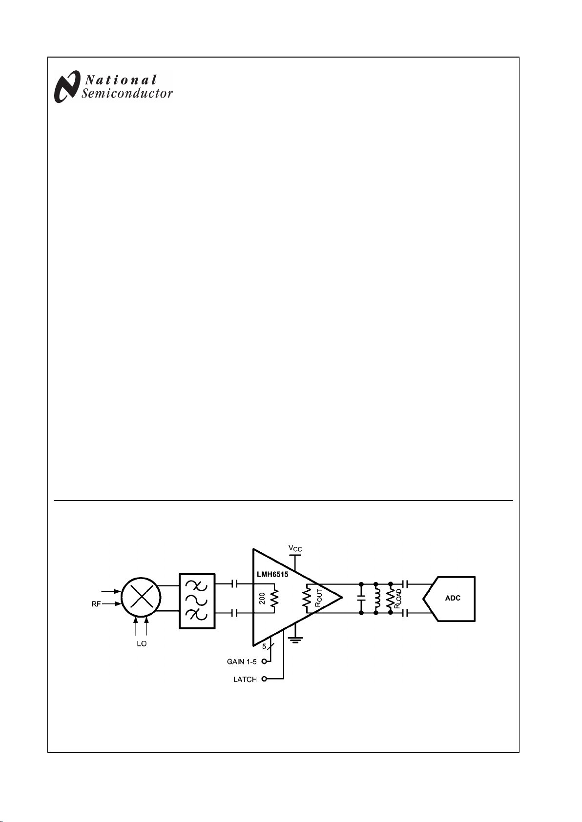
Typical Application
20214301
LMH™ is a trademark of National Semiconductor Corporation.
© 2007 National Semiconductor Corporation 202143 www.national.com
LMH6515 600 MHz, Digital Controlled, Variable Gain Amplifier
Page 2
Absolute Maximum Ratings (Note 1)
If Military/Aerospace specified devices are required,
please contact the National Semiconductor Sales Office/
Distributors for availability and specifications.
ESD Tolerance (Note 2)
Human Body Model 2 kV
Machine Model 150V
Positive Supply Voltage (Pin 3) −0.6V to 5.5V
Output Voltage (pin 14,15) −0.6V to 6.8V
Differential Voltage Between Any
Two Grounds <200 mV
Analog Input Voltage Range −0.6V to V
CC
Digital Input Voltage Range −0.6V to 3.6V
Output Short Circuit Duration
(one pin to ground) Infinite
Junction Temperature +150°C
Storage Temperature Range −65°C to +150°C
Soldering Information
Infrared or Convection (20 sec) 235°C
Wave Soldering (10 sec) 260°C
Operating Ratings (Note 1)
Supply Voltage (Pin 3) 4V to 5.25V
Output Voltage Range (Pin 14, 15) 1.4V to 6.4V
Differential Voltage Between Any
Two Grounds <10 mV
Analog Input Voltage Range,
AC Coupled ±1.4V
Temperature Range (Note 3) −40°C to +85°C
Package Thermal Resistance (θJA)
16-Pin LLP 47°C/W
5V Electrical Characteristics (Note 4)
The following specifications apply for single supply with VCC = 5V, Maximum Gain , RL = 100Ω (200Ω external || 200Ω internal),
V
OUT
= 2 VPP, fin = 150 MHz. Boldface limits apply at temperature extremes.
Symbol Parameter Conditions Min
(Note 6)
Typ
(Note 5)
Max
(Note 6)
Units
Dynamic Performance
SSBW −3 dB Bandwidth Average of all Gain Settings 600 MHz
Noise and Distortion
Third Order Intermodulation
Products
f = 75 MHz, V
OUT
= 2 V
PP
−76
dBc
f = 150 MHz, V
OUT
= 2 V
PP
−72
f = 250 MHz, V
OUT
= 2 V
PP
−66
f = 450 MHz, V
OUT
= 2 V
PP
−58
OIP3 Output 3rd Order Intercept Point f = 75 MHz, V
OUT
= 2 VPP,
Tone Spacing = 0.5 MHz
39
dBm
f = 150 MHz, V
OUT
= 2 VPP,
Tone Spacing = 2 MHz
37
f = 250 MHz, V
OUT
= 2 VPP,
Tone Spacing = 2 MHz
34
f = 75 MHz, RL = 200Ω, V
OUT
= 2 VPP,
Tone Spacing = 0.5 MHz
40
f = 150 MHz, RL = 200Ω, V
OUT
= 2 VPP,
Tone Spacing = 2 MHz
37
f = 250 MHz, RL = 200Ω, V
OUT
= 2 VPP,
Tone Spacing = 2 MHz
34
P1 dB Output Level for 1 dB Gain
Compression
f = 75 MHz, RL = 200Ω
16.7
dBm
f = 250 MHz, RL = 200Ω
14.7
f = 75 MHz 14.5
f = 450 MHz 13.2
VNI Input Noise Voltage Maximum Gain, f = 40 MHz 1.8
nV/
VNO Output Noise Voltage Maximum Gain, f = 40 MHz 18
nV/
NF Noise Figure Maximum Gain 8.3 dB
Analog I/O
Differential Input Resistance 165
160
186 210
220
Ω
Input Common Mode Resistance 825
785
971 1120
1160
Ω
www.national.com 2
LMH6515
Page 3
Symbol Parameter Conditions Min
(Note 6)
Typ
(Note 5)
Max
(Note 6)
Units
Differential Output Impedance Low Gain Option 187
Ω
High Gain Option 330
325
370 410
415
Internal Load Resistors Between Pins 13, 14 and Pins 15, 16 165
160
187 210
235
Ω
Input Signal Level (AC Coupled)
Max Gain, VO = 2 VPP, RL = 1 kΩ
126 mV
PP
Maximum Differential Input Signal AC Coupled 5.6 V
PP
Input Common Mode Voltage Self Biased 1.3
1.1
1.4 1.5
1.7
V
Input Common Mode Voltage
Range
Driven Externally 0.9 to 2.0 V
Minimum Input Voltage DC 0 V
Maximum Input Voltage DC 3.3 V
Maximum Differential Output
Voltage Swing
VCC = 5V, Output Common Mode = 5V 5.5 V
PP
V
OS
Output Offset Voltage All Gain Settings 30 mV
CMRR Common Mode Rejection Ratio 85 dB
PSRR Power Supply Rejection Ratio 63
61
83
dB
Gain Parameters
Maximum Gain
DC, Internal RL = 200Ω,
External RL = 1280Ω
23.9
23.4
24.2 24.6
24.8
dB
Minimum Gain
DC, Internal RL = 200Ω,
External RL = 1280Ω
−7.2
−7.7
−6.9 −6.5
−6.4
dB
Gain Step Size DC 1.0 dB
Gain Step Error DC 0.02
dB
f = 150 MHz 0.07
Cumulative Gain Step Error DC, Gain Step 31 to Gain Step 0 −0.1
−0.2
0.05 0.3
0.4
dB
Gain Step Switching Time 5 ns
Digital Inputs/Timing
Logic Compatibility CMOS Logic 3.3 V
VIL Logic Input Low Voltage 0.8 V
VIH Logic Input High Voltage 2.0 V
IIH Logic Input High Input Current 32 40
μA
TSU Setup Time 3 ns
THOLD Hold Time 3 ns
TPW Minimum Latch Pulse Width 10 ns
Power Requirements
ICC Total Supply Current V
OUT
= 0V Differential, V
OUT
Common
Mode = 5V
107 124
134
mA
Amplifier Supply Current Pin 3 Only 56 66
74
mA
Output Stage Bias Currents Pins 13, 14 and Pins 15, 16;
V
OUT
Common Mode = 5 V
48 58
60
mA
3 www.national.com
LMH6515
Page 4
Note 1: Absolute Maximum Ratings indicate limits beyond which damage to the device may occur. Operating Ratings indicate conditions for which the device is
intended to be functional, but specific performance is not guaranteed. For guaranteed specifications, see the Electrical Characteristics tables.
Note 2: Human Body Model, applicable std. MIL-STD-883, Method 3015.7. Machine Model, applicable std. JESD22-A115-A (ESD MM std. of JEDEC)
Field-Induced Charge-Device Model, applicable std. JESD22-C101-C (ESD FICDM std. of JEDEC).
Note 3: The maximum power dissipation is a function of T
J(MAX)
, θJA. The maximum allowable power dissipation at any ambient temperature is
PD = (T
J(MAX)
– TA)/ θJA. All numbers apply for packages soldered directly onto a PC Board.
Note 4: Electrical Table values apply only for factory testing conditions at the temperature indicated. No guarantee of parametric performance is indicated in the
electrical tables under conditions different than those tested
Note 5: Typical values represent the most likely parametric norm as determined at the time of characterization. Actual typical values may vary over time and will
also depend on the application and configuration. The typical values are not tested and are not guaranteed on shipped production material.
Note 6: Limits are 100% production tested at 25°C. Limits over the operating temperature range are guaranteed through correlation using Statistical Quality
Control (SQC) methods.
Note 7: Negative input current implies current flowing out of the device.
Note 8: Drift determined by dividing the change in parameter at temperature extremes by the total temperature change.
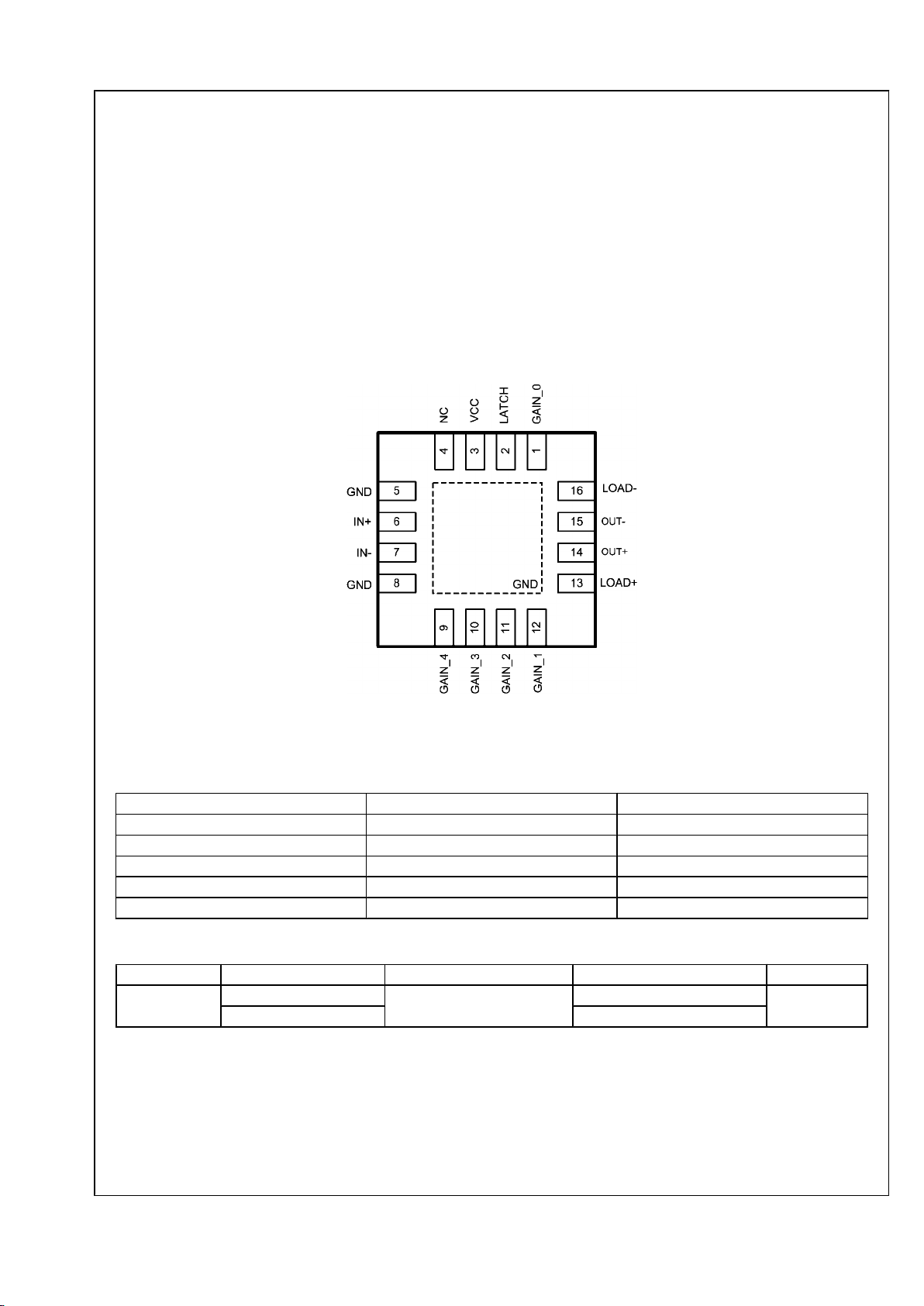
Connection Diagram
16-Pin LLP
20214304
Top View
Gain Control Pins
Pin Number Pin Name Gain Step Size
1 GAIN_0 1 dB
12 GAIN_1 2 dB
11 GAIN_2 4 dB
10 GAIN_3 8 dB
9 GAIN_4 16 dB
Ordering Information
Package Part Number Package Marking Transport Media NSC Drawing
16-Pin LLP
LMH6515SQ
L6515SQ
1k Units Tape and Reel
SQA16A
LMH6515SQX 4.5k Units Tape and Reel
www.national.com 4
LMH6515
Page 5
Pin Descriptions
Pin Number Symbol Description
Analog I/O
6 IN+ Non-inverting analog input. Internally biased to 1.4V. Input voltage should not exceed
VCC or go below GND by more than 0.5V.
7 IN− Inverting analog input. Internally biased to 1.4V. Input voltage should not exceed VCC or
go below GND by more than 0.5V. If using amplifier single ended this input should be
capacitively coupled to ground.
15 OUT− Open collector inverting output. This pin is an output that also requires a power source.
This pin should be connected to 5V through either an RF choke or an appropriately sized
inductor that can form part of a filter. See application section for details.
14 OUT+ Open collector non-inverting output. This pin is an output that also requires a power
source. This pin should be connected to 5V through either an RF choke or an
appropriately sized inductor that can form part of a filter. See application section for
details.
16 LOAD−
Internal 200Ω resistor connection to pin 15. This pin can be left floating for higher gain
or shorted to pin 13 for lower gain and lower effective output impedance. See application
section for details.
13 LOAD+
Internal 200Ω resistor connection to pin 14. This pin can be left floating for higher gain
or shorted to pin 16 for lower gain and lower effective output impedance. See application
section for details.
Power
3 V
CC
5V power supply pin. Use ceramic, low ESR bypass capacitors. This pin powers
everything except the output stage.
5,8 GND Ground pins. Connect to low impedance ground plane. All pin voltages are specified with
respect to the voltage on these pins. The exposed thermal pad is also a ground
connection.
Digital Inputs
1,12,11,
10,9
GAIN_0 to
GAIN_4
Gain setting pins. See above table for gain step sizes for each pin. These pins are 3.3V
CMOS logic compatible. 5V inputs may cause damage.
2 LATCH This pin controls the function of the gain setting pins mentioned above. With LATCH in
the logic HIGH state the gain is fixed and will not change. With the LATCH in the logic
LOW state the gain is set by the state of the gain control pins. Any changes in gain made
with the LATCH pin in the LOW state will take effect immediately. This pin is 3.3V CMOS
logic compatible. 5V inputs may cause damage.
4 NC This pin is not connected. It can be grounded or left floating.
5 www.national.com
LMH6515
Page 6
Typical Performance Characteristics V
CC
= 5V
Frequency Response All Gain Settings
20214322
Frequency Response with Capacitive Load
20214325
Frequency Response Over Temperature, Maximum Gain
20214349
Frequency Response Over Temperature, Minimum Gain
20214350
OIP3 High Gain Mode
20214343
OIP3 Low Gain Mode
20214342
www.national.com 6
LMH6515
Page 7

OIP3 Over Temperature
20214326
OIP3 High Gain Mode
20214324
IMD3 Low Gain Mode
20214340
IMD3 High Gain Mode
20214341
IMD3 High Gain Mode
20214323
HD2 vs. Frequency
20214336
7 www.national.com
LMH6515
Page 8

HD3 vs. Frequency
20214339
HD2 vs. Frequency
20214338
HD3 vs. Frequency
20214337
Noise Figure for All Gain Settings
20214314
Noise Figure vs. Frequency
20214317
Differential Output Noise
20214318
www.national.com 8
LMH6515
Page 9

Maximum Gain vs. Supply Voltage
20214327
Gain vs. External Load
20214312
Maximum Gain Over Temperature
20214344
Worst Case Gain Step Error vs. Frequency
20214345
Worst Case Gain Step Error vs. Frequency
20214346
Worst Case Gain Step Error Over Temperature
20214351
9 www.national.com
LMH6515
Page 10

Digital Crosstalk
20214347
Digital Crosstalk
20214348
Digital Pin to Output Isolation
20214319
Minimum Gain to Maximum Gain Switching
Using Latch Pin
20214330
Maximum Gain to Minimum Gain Switching
Using Latch Pin
20214335
16 dB Gain Step Using Latch Pin
20214332
www.national.com 10
LMH6515
Page 11

16 dB Gain Step with Latch Pin Low
Switching Gain Pin 4
20214329
8 dB Gain Step with Latch Pin Low
Switching Gain Pin 3
20214328
4 dB Gain Step Using Latch Pin
20214333
Power On Timing, Maximum Gain
20214353
Power On Timing, Minimum Gain
20214354
Power Off Timing, Maximum Gain
20214356
11 www.national.com
LMH6515
Page 12
Power Off Timing, Minimum Gain
20214355
Application Information
The LMH6515 is a fully differential amplifier optimized for signal path applications up to 400 MHz. The LMH6515 has a
200Ω input. The absolute gain is load dependent, however
the gain steps are always 1 dB. The LMH6515 output stage
is a class A amplifier. This class A operation results in excellent distortion and linearity characteristics. This makes the
LMH6515 ideal for voltage amplification and an ideal ADC
driver where high linearity is necessary.
20214303
FIGURE 1. LMH6515 Typical Application
The LMH6515 output common mode should be set carefully.
Using inductors to set the output common mode is one preferred method and will give maximum output swing. AC coupling of the output is recommended. The inductors mentioned
above will shift the idling output common mode to the positive
supply. Also, with the inductors, the output voltage can exceed the supply voltage. Other options for setting the output
common mode require supply voltages above 5V. If using a
supply higher than 5V care should be taken to make sure the
output common mode does not exceed the 5.25V supply rating.
It is also important to note the maximum voltage limits for the
OUT+ and OUT− pins, which is 6.4V. When using inductors
these pins will experience voltage swings beyond the supply
voltage. With a 5V output common mode operating point this
makes the effective maximum swing 5.6 VPP differential. System calibration and automatic gain control algorithms should
be tailored to avoid exceeding this limit.
In order to help with system design National Semiconductor
offers the ADC14V155KDRB High IF Receiver reference design board. This board combines the LMH6515 DVGA with
the ADC14V155 ADC and provides a ready made solution for
many IF receiver applications. Using an IF frequency of 169
MHz it achieves a small signal SNR of 72 dBFS and an SFDR
of greater than 90 DBFS. Large signal measurements show
an SNR of 68 dBFS and an SFDR of 77 dBFS. The High IF
Receiver board also features the LMK03000 low-jitter precision clock conditioner.
20214311
FIGURE 2. LMH6515 Block Diagram
INPUT CHARACTERISTICS
The LMH6515 input impedance is set by internal resistors to
a nominal 200Ω. Process variations will result in a range of
values as shown in the 5V Electrical Characteristics table. At
higher frequencies parasitics will start to impact the
impedance. This characteristic will also depend on board layout and should be verified on the customer’s system board.
At maximum gain the digital attenuator is set to 0 dB and the
input signal will be much smaller than the output. At minimum
gain the output is 12 dB or more smaller than the input. In this
configuration the input signal size may limit the amplifier output amplitude, depending on the output configuration and the
desired output signal voltage. The input signal cannot swing
more than 0.5V below the negative supply voltage (normally
0V) nor should it exceed the positive supply voltage. The input
signal will clip and cause severe distortion if it is too large.
Because the input stage self biases to approximately 1.4V the
lower supply voltage will impose the limit for input voltage
swing. To drive larger input signals the input common mode
can be forced higher than 1.4V to allow for more swing. An
www.national.com 12
LMH6515
Page 13

input common mode of 2.0V will allow an 8 VPP maximum
input signal. The trade off for input signal swing is that as the
input common mode is shifted away from the 1.4V internal
bias point the distortion performance will suffer slightly.
20214307
FIGURE 3. Single Ended Input
(Note capacitor on grounded input)
OUTPUT CHARACTERISTICS
The LMH6515 has the option of two different output configurations. The LMH6515 is an open collector topology. As
shown in Figure 8 each output has an on chip 200Ω pull up
resistor. In addition there is an internal 400Ω resistor between
the two outputs. This results in a 200Ω or a 400Ω differential
load in parallel with the external load. The 400Ω option is the
high gain option and the 200Ω provides for less gain. The
200Ω configuration is recommended unless more gain is required.
The output common mode of the LMH6515 must be set by
external components. Most applications will benefit from the
use of inductors on the output stage. In particular, the 400Ω
option, as shown in Figure 9, will require inductors in order to
be able to develop an output voltage. The 200Ω option as
shown in Figure 10 or Figure 11 will also require inductors
since the voltage drop due to the on chip 200Ω resistors will
saturate the output transistors. It is also possible to use resistors and high voltage power supplies to set the output
common mode. This operation is not recommended, unless
it is necessary to DC couple the output. If DC coupling is required the input common mode and output common mode
voltages must be taken into account.
Maximum bandwidth with the LMH6515 is achieved by using
the low gain, low impedance output option and using a low
load resistance. With an effective load of 67Ω a bandwidth of
nearly 1 GHz can be realized. As the effective resistance on
the output stage goes up the capacitance of the board traces
and amplifier output stage limit bandwidth in a roughly linear
fashion. At an output impedance of 100Ω the bandwidth is
down to 600 MHz, and at 200Ω the bandwidth is 260 MHz.
For this reason driving very high impedance loads is not recommended.
Although bandwidth goes down with higher values of load resistance, the distortion performance improves and gain increases. The LMH6515 has a common emitter Class A output
stage and minimizing the amount of current swing in the output devices improves distortion substantially.
The LMH6515 output stage is powered through the collectors
of the output transistors. Power for the output stage is fed
through inductors and the reactance of the inductors allows
the output voltage to develop. In Figure 1 the inductors are
shown with a value of 44.4 nH. The value of the inductors
used will be different for different applications. In Figure 1 the
inductors have been chosen to resonate with the ADC and
the load capacitor to provide a weak band pass filter effect.
For broad band applications higher value inductors will allow
for better low frequency operation. However, large valued inductors will reduce high frequency performance, particularly
inductors of small physical sizes like 0603 or smaller. Larger
inductors will tend to perform better than smaller ones of the
same value even for narrow band applications. This is because the larger inductors will have a lower DC resistance
and less inter-winding capacitance and hence a higher Q and
a higher self resonance frequency. The self resonance frequency should be higher than any desired signal content by
at least a factor of two. Another consideration is that the power
inductors and the filter inductors need to be placed on the
circuit board such that their magnetic fields do not cause coupling. Mutual coupling of inductors can compromise filter
characteristics and lead to unwanted distortion products.
20214315
FIGURE 4. Bandwidth Changes Due to Different Inductor
Values
20214312
FIGURE 5. Gain vs. External Load
DIGITAL CONTROL
The LMH6515 has 32 gain settings covering a range of 31 dB.
To avoid undesirable signal transients the LMH6515 should
be powered on at the minimum gain state (all logic input pins
at 0V). The LMH6515 has a 5-bit gain control bus as well as
a latch pin. When the latch pin is low, data from the gain control pins is immediately sent to the gain circuit (i.e. gain is
changed immediately). When the latch pin transitions high the
13 www.national.com
LMH6515
Page 14

current gain state is held and subsequent changes to the gain
set pins are ignored. To minimize gain change glitches multiple gain control pins should not change while the latch pin is
low. In order to achieve the very fast gain step switching time
of 5 ns the internal gain change circuit is very fast. Gain glitches could result from timing skew between the gain set bits.
This is especially the case when a small gain change requires
a change in state of three or more gain control pins. If continuous gain control is desired the latch pin can be tied to
ground. This state is called transparent mode and the gain
pins are always active. In this state the timing of the gain pin
logic transitions should be planned carefully to avoid undesirable transients.
The LMH6515 was designed to interface with 3.3V CMOS
logic circuits. If operation with 5V logic is required a simple
voltage divider at each logic pin will allow for this. To properly
terminate 100Ω transmission lines a divider with a 66.5Ω resistor to ground and a 33.2Ω series resistor will properly
terminate the line as well as give the 3.3V logic levels. Care
should be taken not to exceed the 3.6V absolute maximum
voltage rating of the logic pins.
EXPOSED PAD LLP PACKAGE
The LMH6515 is in a thermally enhanced package. The exposed pad is connected to the GND pins. It is recommended,
but not necessary, that the exposed pad be connected to the
supply ground plane. In any case, the thermal dissipation of
the device is largely dependent on the attachment of this pad.
The exposed pad should be attached to as much copper on
the circuit board as possible, preferably external copper.
However, it is also very important to maintain good high speed
layout practices when designing a system board. Please refer
to the LMH6515 evaluation board for suggested layout techniques.
Package information is available on the National web site.
http://www.national.com/packaging/folders/sqa16a.html
INTERFACING TO ADC
The LMH6515 was designed to be used with high speed
ADCs such as the ADC14155. As shown in the Typical Application schematic on page 1, AC coupling provides the best
flexibility especially for IF sub-sampling applications. Any resistive networks on the output will also cause a gain loss
because the output signal is developed across the output resistors. The chart Maximum Gain vs. External Load shows the
change in gain when an external load is added.
The inputs of the LMH6515 will self bias to the optimum voltage for normal operation. The internal bias voltage for the
inputs is approximately 1.4V. In most applications the
LMH6515 input will need to be AC coupled.
The output common mode voltage is not self biasing, it needs
to be pulled up to the positive supply rail with external inductors as shown in Figure 1. This gives the LMH6515 the
capability for large signal swings with very low distortion on a
single 5V supply. The internal load resistors provide the
LMH6515 with very consistent gain.
A unique internal architecture allows the LMH6515 to be driven by either a differential or single ended source. If driving the
LMH6515 single ended, the unused input should be terminated to ground with a 0.01 µF capacitor. Directly shorting the
unused input to ground will disrupt the internal bias circuitry
and will result in poor performance.
20214306
FIGURE 6. Bandpass Filter
Center Frequency is 140 MHz with a 20 MHz Bandwidth
Designed for 200Ω Impedance
ADC Noise Filter
Figure 6 shows a filter schematic and the following table of
values are for some common IF frequencies. The filter shown
offers a good compromise between bandwidth, noise rejection and cost. This filter topology is the same as used on the
ADC14V155KDRB High IF Receiver reference design board.
This filter topology works best with the 12 and 14-bit subsampling analog to digital converters shown in the Compati-
ble High Speed Analog to Digital Converters table.
Filter Component Values
Filter Component Values
Fc 75
MHz
140
MHz
170
MHz
250
MHz
BW 40
MHz20MHz25MHz
Narrow
Band
Components L1, L2 10 µH 10 µH 10 µH 10 µH
L3, L4 390 nH 390 nH 560 nH
—
C1, C2 10 pF 3 pF 1.4 pF 47 pF
C3 22 pF 41 pF 32 pF 11 pF
L5 220 nH 27 nH 30 nH 22 nH
R1, R2 100 200 100 499
20214313
FIGURE 7. Sample Filter
www.national.com 14
LMH6515
Page 15

POWER SUPPLIES
As shown in Figure 8, the LMH6515 has a number of options
for power supply connections on the output pins. Pin 3 (VCC)
is always connected. The output stage can be connected as
shown in Figure 9, Figure 10, or Figure 11. The supply voltage
range for VCC is 4V to 5.25V. A 5V supply provides the best
performance while lower supplies will result in less power
consumption. Power supply regulation of 2.5% or better is
advised.
Of special note is that the digital circuits are powered from an
internal supply voltage of 3.3V. The logic pins should not be
driven above the absolute maximum value of 3.6V. See the
Digital Control section for details.
20214302
FIGURE 8. Internal Load Resistors
20214308
FIGURE 9. Using High Gain Mode (400Ω Load)
20214309
FIGURE 10. Using Low Gain Mode (200Ω Load)
20214310
FIGURE 11. Alternate Connection for Low Gain Mode
(200Ω Load)
15 www.national.com
LMH6515
Page 16

Compatible High Speed Analog to Digital Converters
Product Number Max Sampling Rate (MSPS) Resolution Channels
ADC12L063 62 12 SINGLE
ADC12DL065 65 12 DUAL
ADC12L066 66 12 SINGLE
ADC12DL066 66 12 DUAL
CLC5957 70 12 SINGLE
ADC12L080 80 12 SINGLE
ADC12DL080 80 12 DUAL
ADC12C080 80 12 SINGLE
ADC12C105 105 12 SINGLE
ADC12C170 170 12 SINGLE
ADC12V170 170 12 SINGLE
ADC14C080 80 14 SINGLE
ADC14C105 105 14 SINGLE
ADC14DS105 105 14 DUAL
ADC14155 155 14 SINGLE
ADC14V155 155 14 SINGLE
ADC08D500 500 8 DUAL
ADC08500 500 8 SINGLE
ADC08D1000 1000 8 DUAL
ADC081000 1000 8 SINGLE
ADC08D1500 1500 8 DUAL
ADC081500 1500 8 SINGLE
ADC08(B)3000 3000 8 SINGLE
ADC08L060 60 8 SINGLE
ADC08060 60 8 SINGLE
ADC10DL065 65 10 DUAL
ADC10065 65 10 SINGLE
ADC10080 80 10 SINGLE
ADC08100 100 8 SINGLE
ADCS9888 170 8 SINGLE
ADC08(B)200 200 8 SINGLE
ADC11C125 125 11 SINGLE
ADC11C170 170 11 SINGLE
www.national.com 16
LMH6515
Page 17

Physical Dimensions inches (millimeters) unless otherwise noted
16-Pin Package
NS Package Number SQA16A
17 www.national.com
LMH6515
Page 18

Notes
LMH6515 600 MHz, Digital Controlled, Variable Gain Amplifier
THE CONTENTS OF THIS DOCUMENT ARE PROVIDED IN CONNECTION WITH NATIONAL SEMICONDUCTOR CORPORATION
(“NATIONAL”) PRODUCTS. NATIONAL MAKES NO REPRESENTATIONS OR WARRANTIES WITH RESPECT TO THE ACCURACY
OR COMPLETENESS OF THE CONTENTS OF THIS PUBLICATION AND RESERVES THE RIGHT TO MAKE CHANGES TO
SPECIFICATIONS AND PRODUCT DESCRIPTIONS AT ANY TIME WITHOUT NOTICE. NO LICENSE, WHETHER EXPRESS,
IMPLIED, ARISING BY ESTOPPEL OR OTHERWISE, TO ANY INTELLECTUAL PROPERTY RIGHTS IS GRANTED BY THIS
DOCUMENT.
TESTING AND OTHER QUALITY CONTROLS ARE USED TO THE EXTENT NATIONAL DEEMS NECESSARY TO SUPPORT
NATIONAL’S PRODUCT WARRANTY. EXCEPT WHERE MANDATED BY GOVERNMENT REQUIREMENTS, TESTING OF ALL
PARAMETERS OF EACH PRODUCT IS NOT NECESSARILY PERFORMED. NATIONAL ASSUMES NO LIABILITY FOR
APPLICATIONS ASSISTANCE OR BUYER PRODUCT DESIGN. BUYERS ARE RESPONSIBLE FOR THEIR PRODUCTS AND
APPLICATIONS USING NATIONAL COMPONENTS. PRIOR TO USING OR DISTRIBUTING ANY PRODUCTS THAT INCLUDE
NATIONAL COMPONENTS, BUYERS SHOULD PROVIDE ADEQUATE DESIGN, TESTING AND OPERATING SAFEGUARDS.
EXCEPT AS PROVIDED IN NATIONAL’S TERMS AND CONDITIONS OF SALE FOR SUCH PRODUCTS, NATIONAL ASSUMES NO
LIABILITY WHATSOEVER, AND NATIONAL DISCLAIMS ANY EXPRESS OR IMPLIED WARRANTY RELATING TO THE SALE
AND/OR USE OF NATIONAL PRODUCTS INCLUDING LIABILITY OR WARRANTIES RELATING TO FITNESS FOR A PARTICULAR
PURPOSE, MERCHANTABILITY, OR INFRINGEMENT OF ANY PATENT, COPYRIGHT OR OTHER INTELLECTUAL PROPERTY
RIGHT.
LIFE SUPPORT POLICY
NATIONAL’S PRODUCTS ARE NOT AUTHORIZED FOR USE AS CRITICAL COMPONENTS IN LIFE SUPPORT DEVICES OR
SYSTEMS WITHOUT THE EXPRESS PRIOR WRITTEN APPROVAL OF THE CHIEF EXECUTIVE OFFICER AND GENERAL
COUNSEL OF NATIONAL SEMICONDUCTOR CORPORATION. As used herein:
Life support devices or systems are devices which (a) are intended for surgical implant into the body, or (b) support or sustain life and
whose failure to perform when properly used in accordance with instructions for use provided in the labeling can be reasonably expected
to result in a significant injury to the user. A critical component is any component in a life support device or system whose failure to perform
can be reasonably expected to cause the failure of the life support device or system or to affect its safety or effectiveness.
National Semiconductor and the National Semiconductor logo are registered trademarks of National Semiconductor Corporation. All other
brand or product names may be trademarks or registered trademarks of their respective holders.
Copyright© 2007 National Semiconductor Corporation
For the most current product information visit us at www.national.com
National Semiconductor
Americas Customer
Support Center
Email:
new.feedback@nsc.com
Tel: 1-800-272-9959
National Semiconductor Europe
Customer Support Center
Fax: +49 (0) 180-530-85-86
Email: europe.support@nsc.com
Deutsch Tel: +49 (0) 69 9508 6208
English Tel: +49 (0) 870 24 0 2171
Français Tel: +33 (0) 1 41 91 8790
National Semiconductor Asia
Pacific Customer Support Center
Email: ap.support@nsc.com
National Semiconductor Japan
Customer Support Center
Fax: 81-3-5639-7507
Email: jpn.feedback@nsc.com
Tel: 81-3-5639-7560
www.national.com
 Loading...