

Page 1

查询LMH6505供应商
LMH6505
Wideband, Low Power, Linear-in-dB, Variable Gain
Amplifier
LMH6505 Wideband, Low Power, Linear-in-dB, Variable Gain Amplifier
January 2006
General Description
The LMH6505 is a wideband DC coupled voltage controlled
gain stage followed by a high-speed current feedback op
amp which can directly drive a low impedance load. The gain
adjustment range is 80 dB for up to 10 MHz which is accomplished by varying the gain control input voltage, V
Maximum gain is set by external components, and the gain
can be reduced all the way to cut-off. Power consumption is
110 mW with a speed of 150 MHz and a gain control bandwidth (BW) of 100 MHz. Output referred DC offset voltage is
less than 55 mV over the entire gain control voltage range.
Device-to-device gain matching is within
mum gain. Furthermore, gain is tested and guaranteed over
a wide range. The output current feedback op amp allows
high frequency large signals (Slew Rate = 1500 V/µs) and
can also drive a heavy load current (60 mA) guaranteed.
Near ideal input characteristics (i.e. low input bias current,
low offset, low pin 3 resistance) enable the device to be
easily configured as an inverting amplifier as well.
To provide ease of use when working with a single supply,
the V
ground pin potential (pin 4). V
order to ease drive requirement. In single supply operation,
the ground pin is tied to a "virtual" half supply.
The LMH6505’s gain control is linear in dB for a large portion
of the total gain control range from 0 dB down to −85 dB
25˚C, as shown below. This makes the device suitable for
AGC applications. For linear gain control applications, see
the LMH6503 datasheet.
The LMH6505 is available in either the SOIC-8 or the
MSOP-8 package. The combination of minimal external
components and small outline packages allows the
LMH6505 to be used in space-constrained applications.
range is set to be from 0V to +2V relative to the
G
input impedance is high in
G
±
0.5 dB at maxi-
.
G
Features
VS=±5V, TA= 25˚C, RF=1kΩ,RG= 100Ω,RL= 100Ω,A
=A
n −3 dB BW 150 MHz
n Gain control BW 100 MHz
n Adjustment range (
n Gain matching (limit)
n Supply voltage range 7V to 12V
n Slew rate (inverting) 1500 V/µs
n Supply current (no load) 11 mA
n Linear output current
n Output voltage swing
n Input noise voltage 4.4 nV/
n Input noise current 2.6 pA/
n THD (20 MHz, RL= 100Ω,VO=2VPP) −45 dBc
= 9.4 V/V, Typical values unless specified.
VMAX
<
10 MHz) 80 dB
Applications
n Variable attenuator
n AGC
n Voltage controlled filter
n Video imaging processing
@
±
0.50 dB
±
60 mA
±
V
2.4V
Typical Application
A
= 9.4 V/V
VMAX
Gain vs. V
© 2006 National Semiconductor Corporation DS201710 www.national.com
G
20171011
20171002
Page 2

Absolute Maximum Ratings (Note 1)
If Military/Aerospace specified devices are required,
please contact the National Semiconductor Sales Office/
LMH6505
Distributors for availability and specifications.
Junction Temperature 150˚C
Soldering Information:
Infrared or Convection (20 sec) 235˚C
Wave Soldering (10 sec) 260˚C
ESD Tolerance (Note 4)
Human Body Model 2000V
Machine Model 200V
±
Input Current
10 mA
Output Current 120 mA (Note 3)
Supply Voltages (V
Voltage at Input/ Output pins V
+-V−
) 12.6V
+
+0.8V, V−−0.8V
Storage Temperature Range −65˚C to 150˚C
Operating Ratings (Note 1)
Supply Voltages (V
Operating Temperature Range −40˚C to +85˚C
Thermal Resistance: (θ
8 -Pin SOIC 60 165
8-Pin MSOP 65 235
+-V−
) 7Vto12V
)(θJA)
JC
Electrical Characteristics(Note 2)
Unless otherwise specified, all limits are guaranteed for TJ= 25˚C, VS=±5V, A
±
0.1V, RL= 100Ω,VG= +2V. Boldface limits apply at the temperature extremes.
Symbol Parameter Conditions
Frequency Domain Response
BW −3 dB Bandwidth V
GF Gain Flatness V
<
1V
OUT
V
OUT
OUT
<
4VPP,A
<
1V
PP
= 100 38
VMAX
PP
0.9V ≤ VG≤ 2V,±0.2 dB
Att Range Flat Band (Relative to Max Gain)
Attenuation Range (Note 13)
BW
Gain control Bandwidth V
±
0.2 dB Flatness, f<30 MHz 26
±
0.1 dB Flatness, f<30 MHz 9.5
= 1V (Note 12) 100 MHz
G
Control
CT (dB) Feed-through V
= 0V, 30 MHz
G
(Output/Input)
GR Gain Adjustment Range f<10 MHz 80
<
f
30 MHz 71
Time Domain Response
t
r,tf
Rise and Fall Time 0.5V Step 2.1 ns
OS % Overshoot 10 %
SR Slew Rate (Note 5) Non Inverting 900
Inverting 1500
Distortion & Noise Performance
HD2 2
nd
Harmonic Distortion 2VPP, 20 MHz −47
rd
Harmonic Distortion –61
THD Total Harmonic Distortion −45
En tot Total Equivalent Input Noise f
I
N
Input Noise Current f>1 MHz 2.6 pA/
>
1 MHz, R
SOURCE
=50Ω 4.4 nV/
DG Differential Gain f = 4.43 MHz, RL= 100Ω 0.30 %
DP Differential Phase 0.15 deg
DC & Miscellaneous Performance
GACCU Gain Accuracy
(See Application Information)
G Match Gain Matching
(See Application Information)
V
= 2.0V 0
G
<
0.8V
V
G
0.8V
<
V
2V +0.1/−0.53 +4.3/−3.9
G
= 2.0V —
<
<
V
2V — +4.2/−4.0
G
K Gain Multiplier
(See Application Information)
= 9.4 V/V, RF=1kΩ,RG= 100Ω,VIN=
VMAX
Min
(Note 6)
Typ
(Note 6)
Max
(Note 6) Units
150
40 MHz
−51 dB
±
0.50
±
0.50
0.890
0.830
0.940 0.990
1.04
MHz
dB
dB
V/µs
dBcHD3 3
dB
dB
V/V
www.national.com 2
Page 3

Electrical Characteristics(Note 2) (Continued)
Unless otherwise specified, all limits are guaranteed for TJ= 25˚C, VS=±5V, A
±
0.1V, RL= 100Ω,VG= +2V. Boldface limits apply at the temperature extremes.
Symbol Parameter Conditions
NL Input Voltage Range RGOpen
V
IN
V
LR
IN
I
RG_MAX
I
BIAS
TC I
R
IN
C
IN
I
VG
TC I
R
VG
C
VG
V
OUT
V
OUT
R
OUT
I
OUT
V
O
OFFSET
RGCurrent Pin 3
Bias Current Pin 2 (Note 7) −0.6 −2.5
Bias Current Drift Pin 2 (Note 8) –190 pA/˚C
BIAS
Input Resistance Pin 2 7 MΩ
Input Capacitance Pin 2 2.8 pF
VGBias Current Pin 1, VG= 2V (Note 7) 0.9 µA
VGBias Drift Pin 1 (Note 8) 10 pA/˚C
VG
VGInput Resistance Pin 1 25 MΩ
VGInput Capacitance Pin 1 2.8 pF
L Output Voltage Range RL= 100Ω
NL RL= Open
Output Impedance DC 0.12 Ω
Output Current V
Output Offset Voltage 0V<V
+PSRR +Power Supply Rejection Ratio
(Note 9)
−PSRR −Power Supply Rejection Ratio
(Note 9)
I
S
Supply Current No Load 9.5
= 100Ω
G
=±4V from Rails
OUT
<
2V
G
Input Referred, 1V change,
= 2.2V
V
G
Input Referred, 1V change,
= 2.2V
V
G
VMAX
Min
(Note 6)
±
±
±
±
±
±
±
±
–65 –72 dB
–65 –75
= 9.4 V/V, RF=1kΩ,RG= 100Ω,VIN=
0.60
Typ
(Note 6)
±
3
±
0.74
Max
(Note 6) Units
0.50
6.0
±
7.4 mA
5.0
−2.6
2.1
±
2.4
1.9
±
3.1
60
±
80 mA
40
±
10
±
55
±
70
11 14
7.5
16
LMH6505
V
µA
V
mV
dB
mA
www.national.com3
Page 4

Electrical Characteristics(Note 2) (Continued)
Note 1: Absolute Maximum Ratings indicate limits beyond which damage to the device may occur. Operating Ratings indicate conditions for which the device is
intended to be functional, but specific performance is not guaranteed. For guaranteed specifications, see the Electrical Characteristics.
LMH6505
Note 2: Electrical Table values apply only for factory testing conditions at the temperature indicated. Factory testing conditions result in very limited self-heating of
the device such that T
Note 3: The maximum output current (I
Note 4: Human Body Model is 1.5 kΩ in series with 100 pF. Machine Model is 0Ω in series with 200 pF
Note 5: Slew rate is the average of the rising and falling slew rates.
Note 6: Typical values represent the most likely parametric norm. Bold numbers refer to over temperature limits.
Note 7: Positive current corresponds to current flowing into the device.
Note 8: Drift is determined by dividing the change in parameter distribution at temperature extremes by the total temperature change.
Note 9: +PSRR definition: [|∆V
subtracted out.
Note 10: Gain/Phase normalized to low frequency value at 25˚C.
Note 11: Gain/Phase normalized to low frequency value at each setting.
Note 12: Gain control frequency response schematic:
. No guarantee of parametric performance is indicated in the Electrical Tables under conditions of internal self-heating where T
J=TA
OUT
) is determined by device power dissipation limitations or value specified, whichever is lower.
OUT
/∆V+|/AV], −PSRR definition: [|∆V
/∆V−|/AV] with 0.1V input voltage. ∆V
OUT
is the change in output voltage with offset shift
OUT
>
TA.
J
20171016
Note 13: Flat Band Attenuation (Relative To Max Gain) Range Definition: Specified as the attenuation range from maximum which allows gain flatness specified
±
(either
0.2dB or±0.1dB), relative to A
±
0.2 dB: 19.7 dB down to -6.3 dB = 26 dB range
±
0.1 dB: 19.7 dB down to 10.2 dB = 9.5 dB range
gain. For example, for f<30 MHz, here are the Flat Band Attenuation ranges:
VMAX
Connection Diagram
8-Pin SOIC
Top View
20171001
Ordering Information
Package Part Number Package Marking Transport Media NSC Drawing
8-Pin SOIC
8-Pin MSOP
LMH6505MA
LMH6505MAX 2.5k Units Tape and Reel
LMH6505MM
LMH6505MMX 3.5k Units Tape and Reel
LMH6505MA
A93A
95 Units/Rail
1k Units Tape and Reel
M08A
MUA08A
www.national.com 4
Page 5
LMH6505
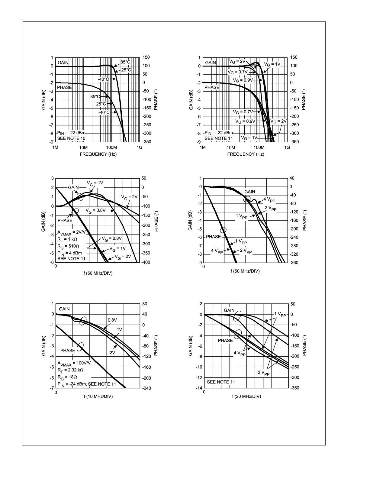
Typical Performance Characteristics Unless otherwise specified: V
V
G=VGMAX,RF
=1kΩ,RG= 100Ω,VIN= 0.1V, input terminated in 50Ω.RL= 100Ω, Typical values.
Frequency Response Over Temperature Frequency Response for Various V
20171003 20171004
Frequency Response (A
= 2) Inverting Frequency Response
VMAX
=±5V, TA= 25˚C,
S
G
Frequency Response for Various VG(A
(Large Signal) Frequency Response for Various Amplitudes
20171046
= 100)
VMAX
20171045 20171064
20171044
www.national.com5
Page 6

Typical Performance Characteristics Unless otherwise specified: V
V
G=VGMAX,RF
LMH6505
=1kΩ,RG= 100Ω,VIN= 0.1V, input terminated in 50Ω.RL= 100Ω, Typical values. (Continued)
Gain Control Frequency Response I
=±5V, TA= 25˚C,
S
vs. V
S
S
20171033
ISvs. V
S
20171020
PSRR A
Input Bias Current vs. V
vs. Supply Voltage
VMAX
20171021
S
20171022
20171034
www.national.com 6
20171023
Page 7

LMH6505
Typical Performance Characteristics Unless otherwise specified: V
V
G=VGMAX,RF
=1kΩ,RG= 100Ω,VIN= 0.1V, input terminated in 50Ω.RL= 100Ω, Typical values. (Continued)
Feed through Isolation for Various A
IRGvs. V
IN
VMAX
20171041
Gain Variation Over entire Temp Range vs. V
=±5V, TA= 25˚C,
S
Gain vs. V
G
G
20171012
20171018
20171011
Output Offset Voltage vs. VG(Typical Unit #1) Output Offset Voltage vs. VG(Typical Unit #2)
20171025
20171030
www.national.com7
Page 8

Typical Performance Characteristics Unless otherwise specified: V
V
G=VGMAX,RF
LMH6505
Output Offset Voltage vs. V
=1kΩ,RG= 100Ω,VIN= 0.1V, input terminated in 50Ω.RL= 100Ω, Typical values. (Continued)
(Typical Unit #3) Distribution of Output Offset Voltage
G
=±5V, TA= 25˚C,
S
20171028
20171061
Output Noise Density vs. Frequency Output Noise Density vs. Frequency
20171008
20171038
Output Noise Density vs. Frequency Input Referred Noise Density vs. Frequency
20171037 20171036
www.national.com 8
Page 9

LMH6505
Typical Performance Characteristics Unless otherwise specified: V
V
G=VGMAX,RF
=1kΩ,RG= 100Ω,VIN= 0.1V, input terminated in 50Ω.RL= 100Ω, Typical values. (Continued)
=±5V, TA= 25˚C,
S
Output Voltage vs. Output Current (Sinking) Output Voltage vs. Output Current (Sourcing)
20171065 20171031
Distortion vs. Frequency HD vs. P
OUT
THD vs. P
OUT
20171042
20171009
THD vs. P
20171043
OUT
20171010
www.national.com9
Page 10

Typical Performance Characteristics Unless otherwise specified: V
V
G=VGMAX,RF
LMH6505
=1kΩ,RG= 100Ω,VIN= 0.1V, input terminated in 50Ω.RL= 100Ω, Typical values. (Continued)
THD vs. Gain THD vs. Gain
=±5V, TA= 25˚C,
S
20171039
Differential Gain & Phase VGBias Current vs. V
20171035
Output Impedance Step Response Plot
20171040
G
20171014
20171062
www.national.com 10
20171015
Page 11

LMH6505
Typical Performance Characteristics Unless otherwise specified: V
V
G=VGMAX,RF
=1kΩ,RG= 100Ω,VIN= 0.1V, input terminated in 50Ω.RL= 100Ω, Typical values. (Continued)
Step Response Plot Gain vs. V
20171017
=±5V, TA= 25˚C,
S
Step
G
20171032
www.national.com11
Page 12

Application Information
GENERAL DESCRIPTION
LMH6505
The key features of the LMH6505 are:
Low power
•
Broad voltage controlled gain and attenuation range
•
(From A
Bandwidth independent, resistor programmable gain
•
range (R
Broad signal and gain control bandwidths
•
Frequency response may be adjusted with R
•
High impedance signal and gain control inputs
•
The LMH6505 combines a closed loop input buffer (“X1”
Block in Figure 1), a voltage controlled variable gain cell
(“MULT” Block) and an output amplifier (“CFA” Block). The
input buffer is a transconductance stage whose gain is set by
the gain setting resistor, R
feedback op amp and is configured as a transimpedance
stage whose gain is set by, and is equal to, the feedback
resistor, R
defined by the ratio:K·R
with a nominal value of 0.940. As the gain control input (V
changes over its 0 to 2V range, the gain is adjusted over a
range of about 80 dB relative to the maximum set gain.
FIGURE 1. LMH6505 Typical Application and Block
down to complete cutoff)
VMAX
)
G
. The output amplifier is a current
G
. The maximum gain, A
F
where “K” is the gain multiplier
F/RG
Diagram
, of the LMH6505 is
VMAX
R
: determines the input voltage range
G
: determines overall bandwidth
R
F
The amount of current which the input buffer can source/sink
into R
is limited and is given in the I
G
RG_MAX
specification.
This sets the maximum input voltage:
Eq. 2
As the I
RG_MAX
F
voltage or with the lowering of R
distortion will increase. Changes in R
limit is approached with increasing the input
, the device’s harmonic
G
will have a dramatic
F
effect on the small signal bandwidth. The output amplifier of
the LMH6505 is a current feedback amplifier (CFA) and its
bandwidth is determined by R
. As with any CFA, doubling
F
the feedback resistor will roughly cut the bandwidth of the
device in half. For more about CFA’s, see the basic tutorial,
OA-20, “Current Feedback Myths Debunked,” or a more
rigorous analysis, OA-13, “Current Feedback Amplifier Loop
Gain Analysis and Performance Enhancements.”
)
G
OTHER CONFIGURATIONS
1) Single Supply Operation
The LMH6505 can be configured for use in a single supply
environment. Doing so requires the following:
a) Bias pin 4 and R
close to the middle of V
is tied to pin 3. The “virtual half supply” needs to be
R
G
to a “virtual half supply” somewhere
G
+
and V−range. The other end of
capable of sinking and sourcing the expected current flow
through R
b) Ensure that V
.
G
can be adjusted from 0V to 2V above the
G
“virtual half supply”.
c) Bias the input (pin 2) to make sure that it stays within the
range of 2V above V
−
to 2V below V+. See the Input
Voltage Range specification in the Electrical Characteristics table. This can be accomplished by either DC biasing
the input and AC coupling the input signal, or alternatively, by direct coupling if the output of the driving stage
is also biased to half supply.
Arranged this way, the LMH6505 will respond to the current
20171047
flowing through R
similar to the split supply arrangement with V
. The gain control relationship will be
G
measured
G
with reference to pin 4. Keep in mind that the circuit described above will also center the output voltage to the
“virtual half supply voltage.”
SETTING THE LMH6505 MAXIMUM GAIN
Eq. 1
Although the LMH6505 is specified at A
recommended A
varies between 2 and 100. Higher
VMAX
= 9.4 V/V, the
VMAX
gains are possible but usually impractical due to output
offsets, noise and distortion. When varying A
VMAX
several
tradeoffs are made:
www.national.com 12
2) Arbitrarily Referenced Input Signal
Having a wide input voltage range on the input (pin 2)
±
3V typical), the LMH6505 can be configured to control the
(
gain on signals which are not referenced to ground (e.g. Half
Supply biased circuits, etc.). We will call this node the “reference node”. In such cases, the other end of R
which is
G
the side not tied to pin 3 can be tied to this reference node so
that R
will “look at” the difference between the signal and
G
this reference only. Keep in mind that the reference node
needs to source and sink the current flowing through R
.
G
Page 13

Application Information (Continued)
GAIN ACCURACY
Gain accuracy is defined as the actual gain compared
against the theoretical gain at a certain V
which are expressed in dB. (See Figure 2).
Theoretical gain is given by:
Eq. 3
Where K = 0.940 (nominal) N = 1.01V & VC=79mV@room
temperature
ForaV
range, the value specified in the tables represents
G
the worst case accuracy over the entire range. The "Typical"
value would be the difference between the "Typical gain" and
the "Theoretical gain." The "Max" value would be the worst
case difference between the actual gain and the "Theoretical
gain" for the entire population.
GAIN MATCHING
As Figure 2 shows, gain matching is the limit on gain variation at a certain V
±
Max" only. There is no "Typical." For a VGrange, the value
"
, expressed in dB, and is specified as
G
specified represents the worst case matching over the entire
range. The "Max" value would be the worst case difference
between the actual gain and the typical gain for the entire
population.
, the results of
G
GAIN PARTITIONING
If high levels of gain are needed, gain partitioning should be
considered:
20171052
FIGURE 3. Gain Partitioning
The maximum gain range for this circuit is given by the
following equation:
Eq. 4
The LMH6624 is a low noise wideband voltage feedback
amplifier. Setting R
gain of 20 dB. Setting R
at 909Ω and R1at 100Ω produces a
2
at 1000Ω as recommended and R
F
at 50Ω, produces a gain of about 26 dB in the LMH6505. The
total gain of this circuit is therefore approximately 46 dB. It is
important to understand that when partitioning to obtain high
levels of gain, very small signal levels will drive the amplifiers
to full scale output. For example, with 46 dB of gain, a 20 mV
signal at the input will drive the output of the LMH6624 to
200 mV and the output of the LMH6505 to 4V. Accordingly,
the designer must carefully consider the contributions of
each stage to the overall characteristics. Through gain partitioning the designer is provided with an opportunity to optimize the frequency response, noise, distortion, settling
time, and loading effects of each amplifier to achieve improved overall performance.
LMH6505
G
20171051
FIGURE 2. LMH6505 Gain Accuracy & Gain Matching
Defined
LMH6505 GAIN CONTROL RANGE AND MINIMUM GAIN
Before discussing Gain Control Range, it is important to
understand the issues which limit it. The minimum gain of the
LMH6505 is theoretically zero, but in practical circuits it is
limited by the amount of feedthrough, here defined as the
gain when V
= 0V. Capacitive coupling through the board
G
and package, as well as coupling through the supplies, will
determine the amount of feedthrough. Even at DC, the input
signal will not be completely rejected. At high frequencies
feedthrough will get worse because of its capacitive nature.
At frequencies below 10 MHz, the feed through will be less
than −60 dB and therefore, it can be said that with
= 20 dB, the gain control range is 80 dB.
A
VMAX
www.national.com13
Page 14

Application Information (Continued)
LMH6505 GAIN CONTROL FUNCTION
LMH6505
In the plot, Gain vs. V
the control voltage. The “Gain (V/V)” plot, sometimes referred to as the S-curve, is the linear (V/V) gain. This is a
hyperbolic tangent relationship and is given by Equation 3.
The “Gain (dB)” plots the gain in dB and is linear over a wide
range of gains. Because of this, the LMH6505 gain control is
referred to as “linear-in-dB.”
For applications where the LMH6505 will be used at the
heart of a closed loop AGC circuit, the S-curve control characteristic provides a broad linear (in dB) control range with
soft limiting at the highest gains where large changes in
control voltage result in small changes in gain. For applications requiring a fully linear (in dB) control characteristic, use
the LMH6505 at half gain and below (V
GAIN STABILITY
The LMH6505 architecture allows complete attenuation of
the output signal from full gain to complete cut-off. This is
achieved by having the gain control signal V
signal which gets through to the final stage and which results
in the output signal. As a consequence, the R
average current (DC current) influences the operating point
of this “throttle” circuit and affects the LMH6505’s gain
slightly. Figure 4 below, shows this effect as a function of the
gain set by V
G
, we can see the gain as a function of
G
G
.
≤ 1V).
G
“throttle” the
pin’s (pin 3)
G
able limits, please refer to the LMH6502 (Differential Linear
in dB variable gain amplifier) datasheet instead at http://
www.national.com/ds/LM/LMH6502.pdf.
AVOIDING OVERDRIVE OF THE LMH6505 GAIN
CONTROL INPUT
There is an additional requirement for the LMH6505 Gain
Control Input (V
): VGmust not exceed +2.3V (with±5V
G
supplies). The gain control circuitry may saturate and the
gain may actually be reduced. In applications where V
G
being driven from a DAC, this can easily be addressed in the
software. If there is a linear loop driving V
, such as an AGC
G
loop, other methods of limiting the input voltage should be
implemented. One simple solution is to place a 2.2:1 resistive divider on the V
is operating off of
exceed 5V and through the divider V
input. If the device driving this divider
G
±
5V supplies as well, its output will not
can not exceed 2.3V.
G
IMPROVING THE LMH6505 LARGE SIGNAL
PERFORMANCE
Figure 5 illustrates an inverting gain scheme for the
LMH6505.
is
20171066
FIGURE 4. LMH6505 Gain Variation over RGDC
Current Capability vs. Gain
This plot shows the expected gain variation for the maximum
DC current capability (±4.5 mA). For example, with gain
R
G
) set to −60 dB, if the RGpin DC current is increased to
(A
V
4.5 mA sourcing, one would expect to see the gain increase
by about 3 dB (to −57 dB). Conversely, 4.5 mA DC sinking
current through R
would increase gain by 1.75 dB (to
G
−58.25 dB). As you can see from Figure 4 above, the effect
is most pronounced with reduced gain and is limited to less
than 3.75 dB variation maximum.
If the application is expected to experience R
DC current
G
variation and the LMH6505 gain variation is beyond accept-
20171054
FIGURE 5. Inverting Amplifier
The input signal is applied through the R
resistor. The V
G
pin should be grounded through a 25Ω resistor. The maximum gain range of this configuration is given in the following
equation:
Eq. 5
The inverting slew rate of the LMH6505 is much higher than
that of the non-inverting slew rate. This ≈ 2X performance
improvement comes about because in the non-inverting configuration the slew rate of the overall amplifier is limited by
the input buffer. In the inverting circuit, the input buffer remains at a fixed voltage and does not affect slew rate.
TRANSMISSION LINE MATCHING
One method for matching the characteristic impedance of a
transmission line is to place the appropriate resistor at the
input or output of the amplifier. Figure 6 shows a typical
circuit configuration for matching transmission lines.
IN
www.national.com 14
Page 15

Application Information (Continued)
FIGURE 6. Transmission Line Matching
LMH6505
20171056
The resistors R
S,RI,RO
istic impedance, Z
to match the output transmission line over a greater
C
O
, and RTare equal to the character-
, of the transmission line or cable. Use
O
frequency range. It compensates for the increase of the op
amp’s output impedance with frequency.
MINIMIZING PARASITIC EFFECTS ON SMALL SIGNAL
BANDWIDTH
The best way to minimize parasitic effects is to use surface
mount components and to minimize lead lengths and component distance from the LMH6505. For designs utilizing
through-hole components, specifically axial resistors, resistor self-capacitance should be considered. For example, the
average magnitude of parasitic capacitance of RN55D 1%
metal film resistors is about 0.15 pF with variations of as
much as 0.1 pF between lots. Given the LMH6505’s extended bandwidth, these small parasitic reactance variations
can cause measurable frequency response variations in the
highest octave. We therefore recommend the use of surface
mount resistors to minimize these parasitic reactance effects.
RECOMMENDATIONS
Here are some recommendations to avoid problems and to
get the best performance:
Do not place a capacitor across RF. However, an appro-
•
priately chosen series RC combination can be used to
shape the frequency response.
Keep traces connecting RFseparated and as short as
•
possible.
Place a small resistor (20-50Ω) between the output and
•
.
C
L
Cut away the ground plane, if any, under RG.
•
Keep decoupling capacitors as close as possible to the
•
LMH6505.
Connect pin 2 through a minimum resistance of 25Ω.
•
ADJUSTING OFFSETS AND DC LEVEL SHIFTING
Offsets can be broken into two parts: an input-referred term
and an output-referred term. These errors can be trimmed
using the circuit in Figure 7. First set V
trim pot R
to null the offset voltage at the output. This will
4
eliminate the output stage offsets. Next set V
adjust the trim pot R
to null the offset voltage at the output.
1
to 0V and adjust the
G
to 2V and
G
This will eliminate the input stage offsets.
20171057
FIGURE 7. Offset Adjust Circuit
DIGITAL GAIN CONTROL
Digitally variable gain control can be easily realized by driving the LMH6505 gain control input with a digital-to-analog
converter (DAC). Figure 8 illustrates such an application.
This circuit employs National Semiconductor’s eight-bit
DAC0830, the LMC8101 MOS input op amp (Rail-to-Rail
Input/Output), and the LMH6505 VGA. With V
REF
set to 2V,
the circuit provides up to 80 dB of gain control in 256 steps
with up to 0.05% full scale resolution. The maximum gain of
this circuit is 20 dB.
www.national.com15
Page 16

Application Information (Continued)
LMH6505
FIGURE 8. Digital Gain Control
20171058
0.25 V
= 100Ω. When the gain is adjusted to −15 dB (i.e. 35 dB
R
G
down from A
in the specified configuration, RF=1kΩ,
PP
), the input amplitude would be 1.41 V
VMAX
PP
and we can see the distortion is at its worst at this gain. If the
output amplitude of the AGC were to be raised above 0.25
, the input amplitudes for gains 40 dB down from A
V
PP
VMAX
would be even higher and the distortion would degrade
further. It is for this reason that we recommend lower output
amplitudes if wide gain ranges are desired. Using a postamp like the LMH6714/LMH6720/LMH6722 family or the
LMH6702 would be the best way to preserve dynamic range
and yield output amplitudes much higher than 100 mV
PP
Another way of addressing distortion performance and its
limitations on dynamic range, would be to raise the value of
. Just like any other high-speed amplifier, by increasing
R
G
the load resistance, and therefore decreasing the demanded
load current, the distortion performance will be improved in
most cases. With an increased R
increased to keep the same A
VMAX
will also have to be
G,RF
and this will decrease the
overall bandwidth. It may be possible to insert a series RC
combination across R
effect on BW when a large R
in order to counteract the negative
F
is used.
F
AUTOMATIC GAIN CONTROL (AGC) #1
.
USING THE LMH6505 IN AGC APPLICATIONS
In AGC applications, the control loop forces the LMH6505 to
have a fixed output amplitude. The input amplitude will vary
over a wide range and this can be the issue that limits
dynamic range. At high input amplitudes, the distortion due
to the input buffer driving R
may exceed that which is
G
produced by the output amplifier driving the load. In the plot,
THD vs. Gain, total harmonic distortion (THD) is plotted over
a gain range of nearly 35 dB for a fixed output amplitude of
Fast Response AGC Loop
The AGC circuit shown in Figure 9 will correcta6dBinput
amplitude step in 100 ns. The circuit includes a two op amp
precision rectifier amplitude detector (U1 and U2), and an
integrator (U3) to provide high loop gain at low frequencies.
The output amplitude is set by R
. The following are some
9
suggestions for building fast AGC loops: Precision rectifiers
work best with large output signals. Accuracy is improved by
blocking DC offsets, as shown in Figure 9.
www.national.com 16
Page 17

Application Information (Continued)
LMH6505
FIGURE 9. Automatic Gain Control Circuit #1
Signal frequencies must not reach the gain control port of the
LMH6505, or the output signal will be distorted (modulated
by itself). A fast settling AGC needs additional filtering beyond the integrator stage to block signal frequencies. This is
provided in Figure 9 by a simple R-C filter (R
and C3);
10
better distortion performance can be achieved with a more
complex filter. These filters should be scaled with the input
signal frequency. Loops with slower response time, which
means longer integration time constants, may not need the
R
10–C3
filter.
Checking the loop stability can be done by monitoring the V
voltage while applying a step change in input signal amplitude. Changing the input signal amplitude can be easily
done with an arbitrary waveform generator.
20171059
AUTOMATIC GAIN CONTROL (AGC) #2
Figure 10 illustrates an automatic gain control circuit that
employs two LMH6505. In this circuit, U1 receives the input
signal and produces an output signal of constant amplitude.
U2 is configured to provide negative feedback. U2 generates
a rectified gain control signal that works against an adjustable bias level which may be set by the potentiometer and
integrates the bias and negative feedback. The result-
R
B.CI
ant gain control signal is applied to the U1 gain control input
. The bias adjustment allows the U1 output to be set at an
V
G
G
arbitrary level less than the maximum output specification of
the amplifier. Rectification is accomplished in U2 by driving
both the amplifier input and the gain control input with the U1
output signal. The voltage divider that is formed by R
, sets the rectifier gain.
R
2
and
1
www.national.com17
Page 18

Application Information (Continued)
LMH6505
FIGURE 10. Automatic Gain Control Circuit #2
20171060
CIRCUIT LAYOUT CONSIDERATIONS & EVALUATION
BOARDS
A good high frequency PCB layout including ground plane
construction and power supply bypassing close to the package are critical to achieving full performance. The amplifier is
sensitive to stray capacitance to ground at the I
-
input (pin 7)
so it is best to keep the node trace area small. Shunt
capacitance across the feedback resistor should not be used
to compensate for this effect. Capacitance to ground should
be minimized by removing the ground plane from under the
body of R
. Parasitic or load capacitance directly on the
G
output (pin 6) degrades phase margin leading to frequency
response peaking.
The LMH6505 is fully stable when driving a 100Ω load. With
reduced load (e.g. 1k.) there is a possibility of instability at
very high frequencies beyond 400 MHz especially with a
capacitive load. When the LMH6505 is connected to a light
load as such, it is recommended to add a snubber network to
the output (e.g. 100Ω and 39 pF in series tied between the
LMH6505 output and ground). C
can also be isolated from
L
the output by placing a small resistor in series with the output
(pin 6).
Component parasitics also influence high frequency results.
Therefore it is recommended to use metal film resistors such
as RN55D or leadless components such as surface mount
devices. High profile sockets are not recommended.
National Semiconductor suggests the following evaluation
board as a guide for high frequency layout and as an aid in
device testing and characterization:
Device Package Evaluation Board
Part Number
LMH6505 SOIC CLC730066
The evaluation board can be shipped when a device sample
request is placed with National Semiconductor. Evaluation
board documentation can be found in the LMH6505 product
folder at www.National.com.
www.national.com 18
Page 19

Physical Dimensions inches (millimeters) unless otherwise noted
8-Pin SOIC
NS Package Number M08A
LMH6505
8-Pin MSOP
NS Package Number MUA08A
www.national.com19
Page 20

Notes
National does not assume any responsibility for use of any circuitry described, no circuit patent licenses are implied and National reserves
the right at any time without notice to change said circuitry and specifications.
For the most current product information visit us at www.national.com.
LIFE SUPPORT POLICY
LMH6505 Wideband, Low Power, Linear-in-dB, Variable Gain Amplifier
NATIONAL’S PRODUCTS ARE NOT AUTHORIZED FOR USE AS CRITICAL COMPONENTS IN LIFE SUPPORT DEVICES OR SYSTEMS
WITHOUT THE EXPRESS WRITTEN APPROVAL OF THE PRESIDENT AND GENERAL COUNSEL OF NATIONAL SEMICONDUCTOR
CORPORATION. As used herein:
1. Life support devices or systems are devices or systems
which, (a) are intended for surgical implant into the body, or
(b) support or sustain life, and whose failure to perform when
properly used in accordance with instructions for use
2. A critical component is any component of a life support
device or system whose failure to perform can be reasonably
expected to cause the failure of the life support device or
system, or to affect its safety or effectiveness.
provided in the labeling, can be reasonably expected to result
in a significant injury to the user.
BANNED SUBSTANCE COMPLIANCE
National Semiconductor manufactures products and uses packing materials that meet the provisions of the Customer Products
Stewardship Specification (CSP-9-111C2) and the Banned Substances and Materials of Interest Specification (CSP-9-111S2) and contain
no ‘‘Banned Substances’’ as defined in CSP-9-111S2.
Leadfree products are RoHS compliant.
National Semiconductor
Americas Customer
Support Center
Email: new.feedback@nsc.com
Tel: 1-800-272-9959
www.national.com
National Semiconductor
Europe Customer Support Center
Fax: +49 (0) 180-530 85 86
Email: europe.support@nsc.com
Deutsch Tel: +49 (0) 69 9508 6208
English Tel: +44 (0) 870 24 0 2171
Français Tel: +33 (0) 1 41 91 8790
National Semiconductor
Asia Pacific Customer
Support Center
Email: ap.support@nsc.com
National Semiconductor
Japan Customer Support Center
Fax: 81-3-5639-7507
Email: jpn.feedback@nsc.com
Tel: 81-3-5639-7560
 Loading...