

Page 1
August 19, 2008
LMH0346
3 Gbps HD/SD SDI Reclocker with Dual Differential Outputs
LMH0346 3 Gbps HD/SD SDI Reclocker with Dual Differential Outputs
General Description
The LMH0346 3 Gbps HD/SD SDI Reclocker retimes serial
digital video data conforming to the SMPTE 424M, SMPTE
292M, and SMPTE 259M (C) standards. The LMH0346 operates at serial data rates of 270 Mbps, 1.483 Gbps, 1.485
Gbps, 2.967 Gbps, and 2.97 Gbps. The LMH0346 supports
DVB-ASI operation at 270 Mbps.
The LMH0346 automatically detects the incoming data rate
and adjusts itself to retime the incoming data to suppress accumulated jitter. The LMH0346 recovers the serial data-rate
clock and optionally provides it as an output. The LMH0346
has two differential serial data outputs; the second output may
be selected as a low-jitter, data-rate clock output. Controls
and indicators are: serial clock or second serial data output
select, manual rate select input, SD/HD rate indicator output,
lock detect output, auto/manual data bypass and output mute.
The serial data inputs, outputs, and serial clock outputs are
differential LVPECL compatible. The CML serial data and serial clock outputs are suitable for driving 100Ω differentially
terminated networks. The control logic inputs and outputs are
LVCMOS compatible.
The LMH0346 is powered from a single 3.3V supply. Power
dissipation is typically 370 mW.
The device is available in two space–saving packages: a 6.5
X 4.4 mm 20-pin e-TSSOP and an even more space–efficient
5 X 4 mm 24-pin LLP package.
Features
Supports SMPTE 424M, SMPTE 292M, and SMPTE
■
259M (C) serial digital video standards
Supports 270 Mbps, 1.483 Gbps, 1.485 Gbps, 2.967
■
Gbps, and 2.97 Gbps serial data rate operation
Supports DVB-ASI at 270 Mbps
■
Single 3.3V supply operation
■
370 mW typical power consumption
■
Two differential, reclocked outputs
■
Choice of second reclocked output or low-jitter,
■
differential, data-rate clock output
Single 27 MHz external crystal or reference clock input
■
Manual or automatic rate select input
■
SD/HD operating rate indicator output
■
Lock Detect indicator output
■
Output mute function for data and clock
■
Auto/Manual reclocker bypass
■
Differential LVPECL compatible serial data inputs and
■
outputs
LVCMOS control inputs and indicator outputs
■
20-pin e-TSSOP or 24-pin LLP package
■
Industrial temperature range: -40°C to +85°C
■
Footprint compatible with the LMH0046
■
andLMH0026 (e-TSSOP package)
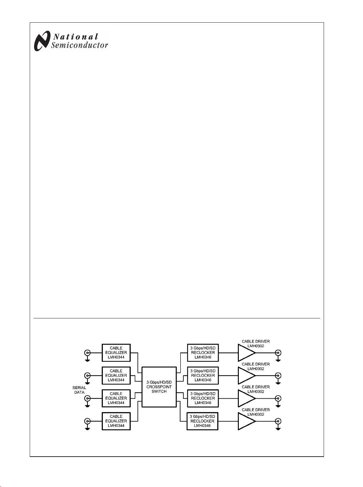
Typical Application
Applications
SDTV/HDTV and 3 Gbps serial digital video interfaces for:
■
Digital video routers and switchers
—
Digital video processing and editing equipment
—
DVB-ASI equipment
—
Video standards and format converters
—
20215001
© 2008 National Semiconductor Corporation 202150 www.national.com
Page 2
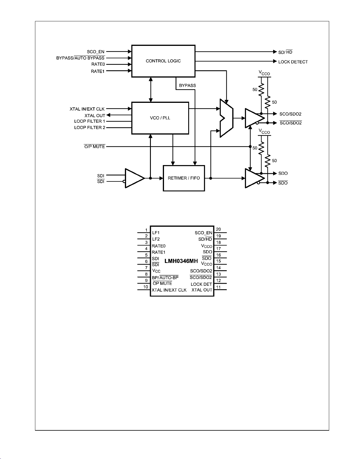
Block Diagram
LMH0346
20215003
Connection Diagrams
The exposed die attach pad is the negative electrical terminal for this device. It must be connected to the negative power supply voltage.
20-Pin e-TSSOP
Order Number LMH0346MH
See NS Package Number MXA20A
20215002
www.national.com 2
Page 3
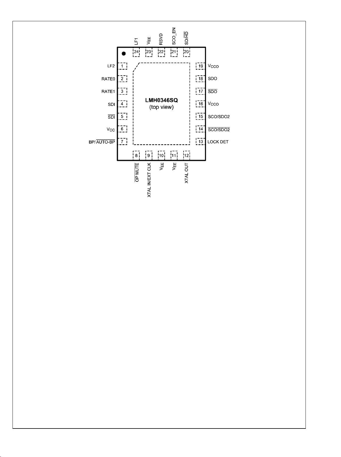
LMH0346
The exposed die attach pad is the primary negative electrical terminal for this device. It must be connected to the negative power supply voltage.
20215006
24-Pin LLP
Order Number LMH0346SQ
See NS Package Number SQA24B
3 www.national.com
Page 4
Pin Descriptions
e-TSSOP
LMH0346
Pin
LLP
Pin
Name Description
1 24 LF1 Loop Filter.
2 1 LF2 Loop Filter.
3 2 RATE 0 Data Rate select input. This pin has an internal pulldown
4 3 RATE 1 Data Rate select input. This pin has an internal pulldown
5 4 SDI Data Input True.
6 5 SDI Data Input Complement.
7 6
V
CC
Positive power supply.
Bypass/Auto Bypass mode select. Bypasses reclocking when high. This pin has
8 7 BYPASS/AUTO BYPASS
an internal pulldown.
Data and Clock Output Mute Input. Mutes the output when low. This pin has an
9 8 OUTPUT MUTE
internal pullup.
10 9 XTAL IN/EXT CLK Crystal or External Oscillator Input.
11 12 XTAL OUT Crystal Oscillator Output.
12 13 LOCK DETECT PLL Lock Detect Output (active high).
13 14 SCO/SDO2 Serial Clock or Serial Data Output 2 Complement.
14 15 SCO/SDO2 Serial Clock or Serial Data Output 2 True.
15 16
V
CCO
Positive power supply (Output Driver).
16 17 SDO Data Output Complement.
17 18 SDO Data Output True.
18 19
V
CCO
Positive power supply (Output Driver).
19 20 SD/HD Data Rate Range Output. Output is high for SD and low for HD or 3G.
Serial Clock or Serial Data 2 Output select. Sets second output to output the clock
20 21 SCO_EN
— 10, 11, 23
V
EE
when high and the data when low. This pin has an internal pulldown.
Negative power supply.
— 22 RSVD Reserved for future use. Do not connect.
DAP DAP
V
EE
Connect exposed DAP to negative power supply (ground).
www.national.com 4
Page 5
LMH0346
Absolute Maximum Ratings (Note 1)
It is anticipated that this device will not be offered in a
military qualified version. If Military/Aerospace specified
devices are required, please contact the National Semiconductor Sales Office/Distributors for availability and specifications.
Supply Voltage (VCC–VEE)
Logic Input Voltage (Vi) VEE−0.15V to V
Logic Input Current (single input):
Vi = VEE−0.15V
Vi = VCC+0.15V
Logic Output Voltage (Vo) VEE−0.15V to V
Logic Output Source/Sink Current ±8 mA
Serial Data Input Voltage (V
Serial Data Output Sink Current (I
) VCC to VCC−2.0V
SDI
)
SDO
4.0V
CC
+0.15V
−5 mA
+5 mA
CC
+0.15V
24 mA
Storage Temp. Range −65°C to +150°C
Junction Temperature +125°C
Lead Temperature (Soldering 4 Sec) +260°C (Pb-free)
ESD Rating (HBM) 8 kV
ESD Rating (MM) 400V
ESD Rating (CDM) 2 kV
Recommended Operating Conditions
Supply Voltage (VCC–VEE)
Logic Input Voltage VEE to V
Differential Serial Input Voltage 800 mV ±10%
Serial Data or Clock Output Sink
Current (ISO)
Operating Free Air Temperature (TA)
3.3V ±5%
16 mA max.
−40°C to +85°C
Package Thermal Resistance
θJA 20-pin e-TSSOP
θJA 24-pin LLP
θJC 20-pin e-TSSOP
θJC 24-pin LLP
26.6°C/W
33.0°C/W
2.4°C/W
3.2°C/W
DC Electrical Characteristics
Over Supply Voltage and Operating Temperature ranges, unless otherwise specified. (Notes 2, 3)
Symbol Parameter Conditions Reference Min Typ Max Units
V
V
V
V
V
V
V
V
V
SDOD
SCOD
I
Input Voltage High Level Logic inputs
IH
Input Voltage Low Level V
IL
I
Input Current High Level VIH = V
IH
I
Input Current Low Level VIL = V
IL
Output Voltage High Level IOH = −2 mA Logic outputs
OH
Output Voltage Low Level IOL = +2 mA
OL
Serial Input Voltage,
SDID
CC
EE
(Note 8) SDI
Differential
Input Common Mode
CMI
V
= 200 mV, (Note 8)
SDID
Voltage
Serial Data Output
100Ω differential load
SDO
Voltage, Differential
Serial Clock Output
Voltage, Differential
Output Common Mode
CMO
100Ω differential load,
2970 Mbps, (Note 8)
100Ω differential load
SCO
SDO, SCO
Voltage
Supply Current 2970 Mbps
CC
2
EE
0.8 V
V
CC
47 65 µA
−18 −25 µA
2 V
VEE + 0.6
200 1600
VEE+1.2
VCC−0.2
620 750 880
400 525 650
VCC−
V
SDOD
V
111 126 mA
mV
mV
mV
V
V
P-P
V
P-P
P-P
CC
5 www.national.com
Page 6

AC Electrical Characteristics
Over Supply Voltage and Operating Temperature ranges, unless otherwise specified. (Note 3)
Symbol Parameter Conditions Reference Min Typ Max Units
LMH0346
BR
BR
BR
TOL
TOL
TOL
TOL
TOL
TOL
t
t
t
BW
F
F
F
F
F
t
T
tr, tfInput rise/fall time 10%–90% Logic inputs
Serial Data Rate SMPTE 259M, C SDI, SDO
SD
Serial Data Rate SMPTE 292M
SD
Serial Data Rate SMPTE 424M
SD
Serial Input Jitter
JIT
Tolerance
Serial Input Jitter
JIT
Tolerance
Serial Input Jitter
JIT
Tolerance
Serial Input Jitter
JIT
Tolerance
Serial Input Jitter
JIT
Tolerance
Serial Input Jitter
JIT
Tolerance
Serial Data Output Jitter 270 Mbps, (Notes 8, 11) SDO
JIT
Serial Data Output Jitter 1483 or 1485 Mbps,
JIT
270 Mbps,
(Notes 7, 8, 9)
270 Mbps,
(Notes 7, 8, 10)
1483 or 1485 Mbps,
(Notes 7, 8, 9)
1483 or 1485 Mbps,
(Notes 7, 8, 10)
2967 or 2970 Mbps,
(Notes 7, 8, 9)
2967 or 2970 Mbps,
(Notes 7, 8, 10)
(Notes 8, 12)
Serial Data Output Jitter 2967 or 2970 Mbps,
JIT
(Notes 8, 13)
Loop Bandwidth 270 Mbps,
LOOP
<0.1dB Peaking
1485 Mbps,
<0.1dB Peaking
2970 Mbps,
<0.1dB Peaking
Serial Clock Output
CO
270 Mbps data rate SCO
Frequency
Serial Clock Output
CO
1483 Mbps data rate
Frequency
Serial Clock Output
CO
1485 Mbps data rate
Frequency
Serial Clock Output
CO
2967 Mbps data rate
Frequency
Serial Clock Output
CO
2970 Mbps data rate
Frequency
Serial Clock Output Jitter
JIT
Serial Clock Output
(Note 8) SDO, SCO
Alignment with respect to
Data Interval
Serial Clock Output Duty
(Note 8) SCO
Cycle
Acquisition Time (Note 6)
ACQ
SDI
270 Mbps
1483,
1485
2967,
2970
Mbps
Mbps
>6
>0.6
>6
>0.6
>6
>0.6
0.01 0.03
0.03 0.04
0.06 0.08
275 kHz
1.5 MHz
2.75 MHz
270 MHz
1483 MHz
1485 MHz
2967 MHz
2970 MHz
2 3
40 60 %
45 55 %
15 ms
1.5 ns
ps
UI
UI
UI
UI
UI
UI
UI
UI
UI
P-P
P-P
P-P
P-P
P-P
P-P
P-P
P-P
P-P
RMS
www.national.com 6
Page 7

Symbol Parameter Conditions Reference Min Typ Max Units
tr, t
tr, t
tr, t
tr, t
tr, t
F
F
Note 1: “Absolute Maximum Ratings” are those parameter values beyond which the life and operation of the device cannot be guaranteed. The stating herein of
these maximums shall not be construed to imply that the device can or should be operated at or beyond these values. The table of “Electrical Characteristics”
specifies acceptable device operating conditions.
Note 2: Current flow into device pins is defined as positive. Current flow out of device pins is defined as negative. All voltages are referenced to VEE (equal to
zero volts).
Note 3: Typical values are stated for: VCC = +3.3V, TA = +25°C.
Note 4: This specification is guaranteed by design.
Note 5: RL = 100Ω differential.
Note 6: Measured from first SDI transition until Lock Detect (LD) output goes high (true).
Note 7: Peak-to-peak amplitude with sinusoidal modulation per SMPTE RP 184-1996 paragraph 4.1. The test data signal shall be color bars.
Note 8: This parameter is guaranteed by characterization over voltage and temperature limits.
Note 9: Refer to “A1” in Figure 1 of SMPTE RP 184-1996.
Note 10: Refer to “A2” in Figure 1 of SMPTE RP 184-1996.
Note 11: PRBS 210−1, input jitter = 31 ps
Note 12: PRBS 210−1, input jitter = 24 ps
Note 13: PRBS 210−1, input jitter = 22 ps
Input rise/fall time 20%–80%, 270 Mbps,
f
(Note 4)
Input rise/fall time 20%–80%, 1483 or 1485
f
Mbps, (Note 4)
Input rise/fall time 20%–80%, 2967 or 2970
f
Mbps, (Note 4)
Output rise/fall time 10%–90% Logic outputs
f
Output rise/fall time 20%–80%, (Notes 5, 8) SDO, SCO
f
REF
Reference Clock
Frequency
TOL
Reference Clock
Frequency Tolerance
P-P
P-P
P-P
SDI
1500 ps
270 ps
135 ps
1.5 ns
90 130 ps
27 MHz
±50 ppm
LMH0346
7 www.national.com
Page 8

Device Description
The LMH0346 3 Gbps HD/SD SDI Reclocker is used in many
types of digital video signal processing equipment. Supported
LMH0346
serial digital video standards are SMPTE 259M (C), SMPTE
292M, and SMPTE 424M. Corresponding serial data rates
are 270 Mbps, 1.483 Gbps, 1.485 Gbps, 2.967 Gbps, and
2.97 Gbps. DVB-ASI data at 270 Mbps may also be retimed.
The LMH0346 retimes the serial data stream to suppress accumulated jitter. It provides two low-jitter, differential, serial
data outputs. The second output may be selected to output
either serial data or a low-jitter serial data-rate clock. Controls
and indicators are: serial clock or second serial data output
select, manual rate select input, SD/HD rate output, lock detect output, auto/manual data bypass and output mute.
Serial data inputs are CML and LVPECL compatible. Serial
data and clock outputs are differential CML and produce
LVPECL compatible levels. The output buffer design can
drive AC or DC-coupled, terminated 100Ω differential loads.
The differential output level is 750 mV
coupled differential loads. Logic inputs and outputs are
LVCMOS compatible.
The device package is a 20-pin e-TSSOP or a 24-pin LLP.
Both package options have an exposed die attach pad. The
exposed die attach pad is electrically connected to device
ground (VEE) and is the negative electrical terminal for the
device. This terminal must be connected to the negative power supply or circuit ground.
into 100Ω AC or DC-
P-P
Serial Data Inputs, Serial Data and Clock Outputs
SERIAL DATA INPUT AND OUTPUTS
The differential serial data input, SDI, accepts serial digital
video data at the rates specified in Table 1. The serial data
input is differential LVPECL compatible. The input is intended
to be DC interfaced to devices such as the LMH0344 adaptive
cable equalizer. The input is not internally terminated or biased. The input may be AC-coupled if a suitable input bias
voltage is provided. Figure 1 shows the equivalent input circuit
for SDI and SDI
The LMH0346 has two, retimed, differential, serial data outputs, SDO and SCO/SDO2. These outputs provide low jitter,
differential, retimed data to devices such as the LMH0302
cable driver. Output SCO/SDO2 is multiplexed and can provide either a second serial data output or a serial clock output.
Figure 2 shows the equivalent output circuit for SDO, SDO,
SCO/SDO2, and SCO/SDO2.
The SCO_EN input controls the operating mode for the SCO/
SDO2 output. When the SCO_EN input is high the SCO/
SDO2 output provides a serial clock. When SCO_EN is low,
the SCO/SDO2 output provides retimed serial data.
Both differential serial data outputs, SDO and SCO/SDO2,
are muted when the OUTPUT MUTE input is a logic low level.
SCO/SDO2 also mutes when the Bypass mode is activated
and this output is operating as the serial clock output
(SCO_EN input is high). When muted, SDO and SDO (or
SDO2 and SDO2) will assume opposite differential output
levels. The CML serial data outputs are differential LVPECL
compatible. These outputs have internal 50Ω pull-ups and are
suitable for driving AC or DC-coupled, 100Ω center-tapped,
AC grounded or 100Ω un-center-tapped, differentially terminated networks.
.
FIGURE 1. Equivalent SDI Input Circuit (SDI, SDI)
www.national.com 8
20215008
Page 9

20215009
FIGURE 2. Equivalent SDO Output Circuit (SDO, SDO, SCO/SDO2, SCO/SDO2)
LMH0346
OPERATING SERIAL DATA RATES
This device operates at serial data rates of 270 Mbps, 1483
Mbps, 1485 Mbps, 2967 Mbps, and 2970 Mbps. The device
does not lock to harmonics of these rates. The device does
not lock and automatically enters the reclocker bypass mode
for the following data rates: 143 Mbps, 177 Mbps, 360 Mbps,
and 540 Mbps.
SERIAL DATA CLOCK/SERIAL DATA 2 OUTPUT
The Serial Data Clock/Serial Data 2 Output is controlled by
the SCO_EN input and provides either a second retimed serial data output or a low jitter differential clock output appropriate to the serial data rate being processed. When operating
as a serial clock output, the rising edge of the clock will be
positioned within the corresponding serial data bit interval
within 10% of the center of the data interval.
Differential output SCO/SDO2 functions as the second serial
data output when the SCO_EN input is a logic-low level. This
output functions as the serial clock output when the SCO_EN
input is a logic-high level. The SCO_EN input has an internal
pull-down device and the default state of SCO_EN is low (serial data output 2 enabled). SCO/SDO2 is muted when the
OUTPUT MUTE
mode is activated and this output is functioning as a serial
clock output (SCO_EN is high), the output will also be muted.
If an unsupported data rate is used while in Auto Bypass mode
with this output functioning as a serial clock output, the output
is invalid.
input is a logic low level. When the Bypass
Control Inputs and Indicator Outputs
SERIAL DATA RATE SELECTOR
The Serial Data Rate Selector (RATE [1:0]) permits the user
to fix the operating serial data rate. The pins have internal pulldowns which maintain a logic-low input condition unless externally driven to a logic-high condition. This input also serves
to place the device in a test mode. The codes shown in
Table 1 select the desired operating serial data rate. The
LMH0346 then enters either the Auto-Rate Detect mode or a
single operating rate. Selecting the 270 Mbps rate mode may
also be used when reclocking DVB-ASI data. DVB-ASI data
is MPEG2 coded data that is transmitted in 8B10B coding.
The device will reclock this data without harmonic locking.
Auto-Rate Detect mode may be used for any supported data
rate, including DVB-ASI.
TABLE 1. Data Rate Select Input Codes
Rate [1:0]
Code
00 Auto-Rate
01 270 Mbps May be used to support DVB-
10 1483/1485
LOCK DETECT
The Lock Detect (LD) output, when high, indicates that data
is being received and the PLL is locked. LD may be connected
to the OUTPUT MUTE input to mute the data and clock outputs when no data signal is being received. Note that when
the Bypass/Auto Bypass input is set high, Lock Detect will
remain low. See Table 2.
OUTPUT MUTE
The OUTPUT MUTE input, when low, mutes the serial data
and clock outputs. It may be connected to Lock Detect or externally driven to mute or un-mute the outputs. If OUTPUT
MUTE is connected to LD, then the data and clock outputs
are muted when the PLL is not locked. This function overrides
the Bypass function: see Table 2. OUTPUT MUTE has an
internal pull-up device to enable the output by default.
BYPASS/AUTO BYPASS
The Bypass/Auto Bypass input, when high, forces the device
to output the data without reclocking it. When this input is low,
the device automatically bypasses the reclocking function
when the device is in an unlocked condition or the detected
data rate is a rate which the device does not support. Note
that when the Bypass/Auto Bypass input is set high, Lock
Detect will remain low. See Table 2. BYPASS/AUTO BYPASS has an internal pull-down device.
Data Rate
or Mode
Detect
mode
Mbps,
2967/2970
Mbps
Comments
ASI operation
9 www.national.com
Page 10

TABLE 2. Control Functionality
LOCK DETECT OUTPUT MUTE BYPASS/AUTO BYPASS DEVICE STATUS
LMH0346
0 1 X PLL unlocked, reclocker bypassed
1 1 0 PLL locked to supported data rate, reclocker not bypassed
X 0 X Outputs muted
0 LOCK DETECT X Outputs muted
1 LOCK DETECT 0 PLL locked to supported data rate, reclocker not bypassed
SD/HD
The SD/HD output indicates whether the LMH0346 is processing SD or HD / 3 Gbps data rates. It may be used to
control another device such as the LMH0302 cable driver.
When this output is high it indicates that the data rate is 270
Mbps. When low, the indicated data rate is 1483, 1485, 2967,
or 2970 Mbps. The SD/HD output is a registered function and
is only valid when the PLL is locked and the Lock Detect output is high. When the PLL is not locked (the Lock Detect
output is low), the SD/HD output defaults to HD (low). The SD/
HD output is undefined for a short time after lock detect assertion or deassertion due to a data rate change on SDI. See
Figure 3 for a timing diagram showing the relationship between SDI, Lock Detect, and SD/HD.
FIGURE 3. SDI, Lock Detect, and SD/HD Timing
www.national.com 10
20215005
Page 11

LMH0346
SCO_EN
Input SCO_EN enables the SCO/SDO2 differential output to
function either as a serial clock or second serial data output.
SCO/SDO2 functions as a serial clock when SCO_EN is high.
This pin has an internal pull-down device. The default state
(low) enables the SCO/SDO2 output as a second serial data
output.
CRYSTAL OR EXTERNAL CLOCK REFERENCE
The LMH0346 uses a 27 MHz crystal or external clock signal
as a timing reference input. A 27 MHz parallel resonant crystal
and load network may be connected to the XTAL IN/EXT CLK
and XTAL OUT pins. Alternatively, a 27 MHz LVCMOS compatible clock signal may be input to XTAL IN/EXT CLK. Parameters for a suitable crystal are given in Table 3.
TABLE 3. Crystal Parameters
Parameter Value
Frequency 27 MHz
Frequency Stability ±50 ppm @
recommended drive level
Parameter Value
Operating Mode Fundamental mode,
Parallel Resonant
Load Capacitance 18–20 pF
Shunt Capacitance 7 pF
Series Resistance
Recommended Drive Level 100 µW
Maximum Drive Level 500 µW
Operating Temperature Range −10°C to +60°C
40Ω max.
11 www.national.com
Page 12

Application Information
Figure 4 shows an application circuit for the LMH0346 along
with the LMH0344 3 Gbps HD/SD SDI Adaptive Cable Equal-
LMH0346
izer and LMH0302 3 Gbps HD/SD SDI Cable Driver.
FIGURE 4. Application Circuit
The LMH0346 inputs are LVPECL compatible. The LMH0346
has a wide input common mode range and in most cases the
input should be DC coupled. For DC coupling, the inputs must
be kept within the common mode range specified in DC Elec-
trical Characteristics. Figure 4 shows an example of a DC
coupled interface between the LMH0344 cable equalizer and
the LMH0346. The LMH0344 output common mode voltage
and voltage swing are within the range of the input common
mode voltage and voltage swing of the LMH0346. All that is
www.national.com 12
20215004
required is a 100Ω differential termination as shown. The resistor should be placed as close to the LMH0346 input as
possible. If desired, this network may be terminated with two
50Ω resisters and a center tap capacitor to ground in place of
the single 100Ω resistor.
The LMH0346 outputs are LVPECL compatible. SDO is the
primary data output and SCO/SDO2 is a second output that
may be set as the serial clock or a second data output. Both
outputs are always active. The LMH0346 output should be
Page 13

LMH0346
DC coupled to the input of the receiving device as long as the
common mode ranges of both devices are compatible. Figure
4 shows an example of a DC coupled interface between the
LMH0346 and LMH0302 cable driver. All that is required is a
100Ω differential termination as shown. The resistor should
be placed as close to the LMH0302 input as possible. If desired, this network may be terminated with two 50Ω resisters
and a center tap capacitor to ground in place of the single
100Ω resistor.
The external loop filter capacitor (between LF1 and LF2)
should be 56 nF. This is the only supported value; the loop
filter capacitor should not be changed.
RATE0 and RATE1 have internal pulldowns to select AutoRate Detect mode by default. These pins may also be used
to set the device to SD mode or HD/3G mode.
BYPASS/AUTO BYPASS has an internal pulldown to enable
Auto Bypass mode by default. This pin may be pulled high to
force the LMH0346 to bypass all data.
OUTPUT MUTE has an internal pullup to enable the outputs
by default. This pin may be pulled low to mute the outputs.
The XTAL IN/EXT CLK and XTAL OUT pins are shown with
a 27 MHz crystal and the proper loading. The crystal should
match the parameters described in Table 3. Alternately, a
27MHz LVCMOS compatible clock signal may be input to
XTAL IN/EXT CLK.
The active high LOCK DETECT output provides an indication
that proper data is being received and the PLL is locked.
The SD/HD output may be used to drive the SD/HD pin of an
SDI cable driver (such as the LMH0302) in order to properly
set the cable driver’s edge rate for SMPTE compliance. It defaults to HD/3G (low) when the LMH0346 is not locked.
SCO_EN has an internal pulldown to set the second output
(SCO/SDO2) to output data. This pin may be pulled high to
set the second output as a serial clock.
The ground connection for the LMH0346 is through the large
exposed DAP. The DAP must be connected to ground for
proper operation of the LMH0346. This is the only ground
connection for the LMH0346MH. It is the primary ground connection, required for good signal integrity, for the
LMH0346SQ.
13 www.national.com
Page 14

Physical Dimensions inches (millimeters) unless otherwise noted
LMH0346
20-Pin e-TSSOP
Order Number LMH0346MH
NS Package Number MXA20A
Order Number LMH0346SQ
NS Package Number SQA24B
www.national.com 14
24-Pin LLP
Page 15

Notes
LMH0346
15 www.national.com
Page 16

Notes
For more National Semiconductor product information and proven design tools, visit the following Web sites at:
Products Design Support
Amplifiers www.national.com/amplifiers WEBENCH www.national.com/webench
Audio www.national.com/audio Analog University www.national.com/AU
Clock Conditioners www.national.com/timing App Notes www.national.com/appnotes
Data Converters www.national.com/adc Distributors www.national.com/contacts
Displays www.national.com/displays Green Compliance www.national.com/quality/green
Ethernet www.national.com/ethernet Packaging www.national.com/packaging
Interface www.national.com/interface Quality and Reliability www.national.com/quality
LVDS www.national.com/lvds Reference Designs www.national.com/refdesigns
Power Management www.national.com/power Feedback www.national.com/feedback
Switching Regulators www.national.com/switchers
LDOs www.national.com/ldo
LED Lighting www.national.com/led
PowerWise www.national.com/powerwise
Serial Digital Interface (SDI) www.national.com/sdi
Temperature Sensors www.national.com/tempsensors
Wireless (PLL/VCO) www.national.com/wireless
THE CONTENTS OF THIS DOCUMENT ARE PROVIDED IN CONNECTION WITH NATIONAL SEMICONDUCTOR CORPORATION
(“NATIONAL”) PRODUCTS. NATIONAL MAKES NO REPRESENTATIONS OR WARRANTIES WITH RESPECT TO THE ACCURACY
OR COMPLETENESS OF THE CONTENTS OF THIS PUBLICATION AND RESERVES THE RIGHT TO MAKE CHANGES TO
SPECIFICATIONS AND PRODUCT DESCRIPTIONS AT ANY TIME WITHOUT NOTICE. NO LICENSE, WHETHER EXPRESS,
IMPLIED, ARISING BY ESTOPPEL OR OTHERWISE, TO ANY INTELLECTUAL PROPERTY RIGHTS IS GRANTED BY THIS
DOCUMENT.
TESTING AND OTHER QUALITY CONTROLS ARE USED TO THE EXTENT NATIONAL DEEMS NECESSARY TO SUPPORT
NATIONAL’S PRODUCT WARRANTY. EXCEPT WHERE MANDATED BY GOVERNMENT REQUIREMENTS, TESTING OF ALL
PARAMETERS OF EACH PRODUCT IS NOT NECESSARILY PERFORMED. NATIONAL ASSUMES NO LIABILITY FOR
APPLICATIONS ASSISTANCE OR BUYER PRODUCT DESIGN. BUYERS ARE RESPONSIBLE FOR THEIR PRODUCTS AND
APPLICATIONS USING NATIONAL COMPONENTS. PRIOR TO USING OR DISTRIBUTING ANY PRODUCTS THAT INCLUDE
NATIONAL COMPONENTS, BUYERS SHOULD PROVIDE ADEQUATE DESIGN, TESTING AND OPERATING SAFEGUARDS.
EXCEPT AS PROVIDED IN NATIONAL’S TERMS AND CONDITIONS OF SALE FOR SUCH PRODUCTS, NATIONAL ASSUMES NO
LIABILITY WHATSOEVER, AND NATIONAL DISCLAIMS ANY EXPRESS OR IMPLIED WARRANTY RELATING TO THE SALE
AND/OR USE OF NATIONAL PRODUCTS INCLUDING LIABILITY OR WARRANTIES RELATING TO FITNESS FOR A PARTICULAR
PURPOSE, MERCHANTABILITY, OR INFRINGEMENT OF ANY PATENT, COPYRIGHT OR OTHER INTELLECTUAL PROPERTY
RIGHT.
LMH0346 3 Gbps HD/SD SDI Reclocker with Dual Differential Outputs
LIFE SUPPORT POLICY
NATIONAL’S PRODUCTS ARE NOT AUTHORIZED FOR USE AS CRITICAL COMPONENTS IN LIFE SUPPORT DEVICES OR
SYSTEMS WITHOUT THE EXPRESS PRIOR WRITTEN APPROVAL OF THE CHIEF EXECUTIVE OFFICER AND GENERAL
COUNSEL OF NATIONAL SEMICONDUCTOR CORPORATION. As used herein:
Life support devices or systems are devices which (a) are intended for surgical implant into the body, or (b) support or sustain life and
whose failure to perform when properly used in accordance with instructions for use provided in the labeling can be reasonably expected
to result in a significant injury to the user. A critical component is any component in a life support device or system whose failure to perform
can be reasonably expected to cause the failure of the life support device or system or to affect its safety or effectiveness.
National Semiconductor and the National Semiconductor logo are registered trademarks of National Semiconductor Corporation. All other
brand or product names may be trademarks or registered trademarks of their respective holders.
Copyright© 2008 National Semiconductor Corporation
For the most current product information visit us at www.national.com
www.national.com
National Semiconductor
Americas Technical
Support Center
Email: support@nsc.com
Tel: 1-800-272-9959
National Semiconductor Europe
Technical Support Center
Email: europe.support@nsc.com
German Tel: +49 (0) 180 5010 771
English Tel: +44 (0) 870 850 4288
National Semiconductor Asia
Pacific Technical Support Center
Email: ap.support@nsc.com
National Semiconductor Japan
Technical Support Center
Email: jpn.feedback@nsc.com
 Loading...