

Page 1
ADVANCE INFORMATION
June 2007
LMH0341, LMH0041, LMH0071, LMH0051
3G, HD, SD, DVB-ASI SDI Deserializer with Loopthrough
and LVDS Interface
General Description
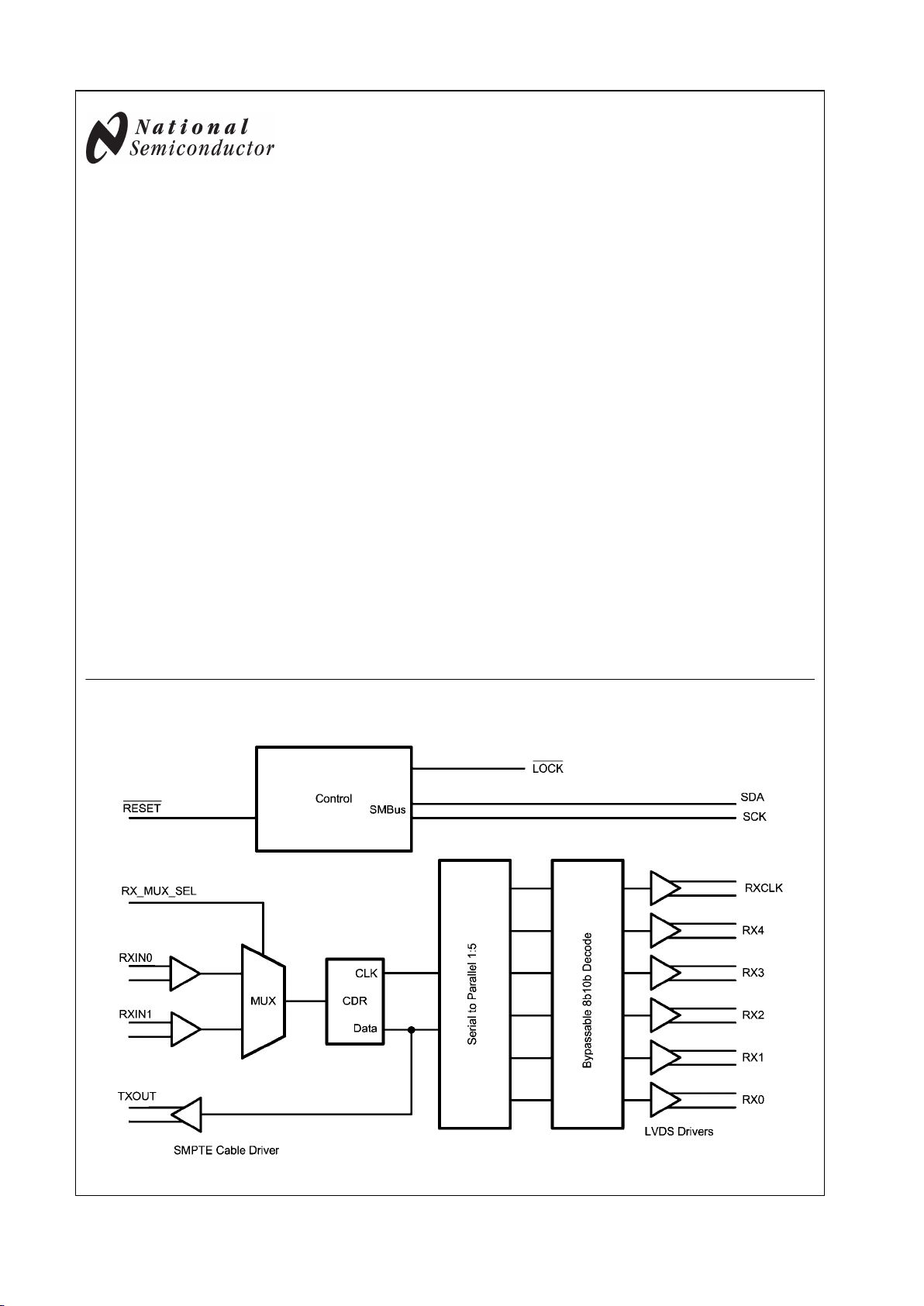
The LMH0041 family of products provide a very simple 1:5
deserializer and receiver function. The device is intended to
be paired with an FPGA host which will receive the raw 5 bit
data words and will decode the data appropriately such that
a SMPTE standard signal may be recovered. The devices are
designed to receive data compliant with DVB-ASI, SMPTE
259M, SMPTE 292M and/or SMPTE 424M. The interface between the LMH0041 and the FPGA consists of a 5 bit wide
LVDS bus, an LVDS clock and an SMBus interface. All devices except for the LMH0051 includes a reclocked
feedthrough output with a SMPTE compliant cable driver. The
LMH0341 includes support for SMPTE424M, and the
LMH0071 is a Stadard Definition (SD) only variant. The product is packaged in a physically small 48 pin LLP package.
Key Specifications
■
Output compliant with SMPTE 259M-C, SMPTE 292M,
SMPTE 424M and DVB-ASI
■
Typical power dissipation: 410 mW (loopthrough disabled)
■
0.6 UI Input Jitter Tolerance
Features
■
LVDS Interface
■
Dual multiplexed inputs
■
No external VCO or clock required
■
Loopthrough with Cable Driver
■
SMBus configuration interface
■
48 pin LLP package
Applications
■
SDI interfaces for:
—
Video Cameras
—
DVRs
—
Video Switchers
—
Video Editing Systems
Block Diagram
30017201
© 2007 National Semiconductor Corporation 300172 www.national.com
LMH0341, LMH0041, LMH0071, LMH0051 3G, HD, SD, DVB-ASI SDI Deserializer with
Loopthrough and LVDS Interface
Page 2
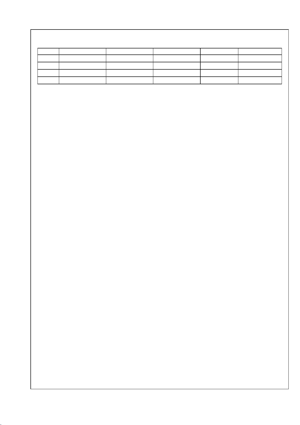
TABLE 1. Feature Table
Device SMPTE 424M Support SMPTE 292M Support SMPTE 259M Support DVB-ASI Support Active Loopthrough
LMH0341
× × × × ×
LMH0041
× × × ×
LMH0071
× × ×
LMH0051
× × ×
www.national.com 2
LMH0341, LMH0041, LMH0071, LMH0051
Page 3
Absolute Maximum Ratings (Note 1)
If Military/Aerospace specified devices are required,
please contact the National Semiconductor Sales Office/
Distributors for availability and specifications.
Supply Voltage (VCC)
−0.3V to +4.0V
LVCMOS (SMBus) input voltage −0.3V to (VCC+0.3V)
LVCMOS (SMBus) output voltage −0.3V to (VCC+0.3V)
LVDS Input Voltage 0.3V to 3.6V
Junction Temperature +150°C
Storage Temperature −65° to 150°C
Lead Temperature—Soldering 4 seconds +260°C
Thermal Resistance—
Junction to Ambient—θ
JA
40°C/W
ESD Rating—Human Body Model,
1.5 KΩ, 100 pF 4KV
Recommended Operating Conditions
Parameter Min Typ Max Units
Supply Voltage (VCC-GND) 3.1 3.3 3.5 V
2.4 2.5 2.6 V
Supply noise amplitude (10 Hz to 50 MHz) 100 mV
P-P
Ambient Temperature −40 +25 +85 °C
Case Temperature 100 °C
LVDS PCB board trace length (mismatch <2%) 25 cm
LMH0041 Electrical Characteristics Over supply and Operating Temperature ranges unless otherwise
specified
Symbol Parameter Condition Min
Typ
(Note 2)
Max Units
I
DD2.5
2.5V supply current mA
I
DD3.3
3.3V supply current 106 mA
P
D
Power Consumption VDD = 3.6V All outputs
terminated by 100Ω, 2.97 Gbps
output, loopthrough disabled
410 mW
Loopthrough enabled 475 mW
Control Pin Electrical Characteristics Over supply and Operating Temperature ranges unless otherwise
specified. Applies to MODE0, MODE1, RESET and LOCK
Symbol Parameter Condition Min
Typ
(Note 2)
Max Units
V
IH
High Level Input Voltage 2.0 VCC +0.3 V
V
IL
Low Level Input Voltage −0.3 0.8 V
V
OH
High Level Output Voltage IOH = −0.4 mA 2.7 3.3 V
IOH = −2 mA 2.7 2.85 V
V
OL
Low Level Output Voltage IOL = 2 mA 0.1 0.3 V
V
CL
Input Clamp Voltage ICL = −18 mA −0.79 −1.5 V
I
IN
Input Current VIN = 0.4V, 2.5V or V
DD
1.8 15
μA
VIN = GND −15 0
μA
I
OS
Output Short Circuit Current V
OUT
= 0V −120 mA
3 www.national.com
LMH0341, LMH0041, LMH0071, LMH0051
Page 4
LVDS Output Electrical Characteristics Over supply and Operating Temperature ranges unless
otherwise specified
Symbol Parameter Condition Min
Typ
(Note 2)
Max Units
V
OD
Differential Output Voltage
RL = 100Ω
250 345 459 mV
ΔV
OD
Change in VOD between
complementary output states
35 mV
V
OS
Offset Voltage 1.125 1.25 1.375 V
ΔV
OS
Change in VOS between
complementary output states
35 mV
I
OS
Output Short Circuit Current
V
OUT
= 0V, RL = 100Ω
50 mA
I
OZ
Output TRI-state current PD = 0V, V
OUT
= 0V or V
CC
±1 ±10
μA
SMBus Input Electrical Characteristics Over supply and Operating Temperature ranges unless
otherwise specified
Symbol Parameter Condition Min
Typ
(Note 2)
Max Units
V
SIL
Data, Clock Input Low Voltage 0.8 V
V
SIH
Data, Clock Input High Voltage 2.1 V
SDD
V
I
SPULLUP
Current through pull-up resistor or
current source
4 mA
V
SDD
Nominal Bus Voltage 2.375 3.6 V
I
SLEAKB
Input Leakage per bus segment See (Note 3) −200 200
μA
I
SLEAKP
Input Leakage per pin −10 10
μA
C
SI
Capacitance for SMBdata and
SMBclk
See (Notes 3, 4) 10 pF
R
STERM
Termination Resistance V
SDD3.3
See (Notes 3, 4, 5) 2000
Ω
V
SDD3.3
See (Notes 3, 4, 5) 1000
Ω
LVDS Switching Characteristics
Symbol Parameter Condition Min
Typ
(Note 2)
Max Units
t
ROTR
LVDS Low to High Transition time See Figure 1 LVDS Switching
times
0.2T 3 ns
t
ROTF
LVDS High to Low Transition time 0.2T 3 ns
t
ROCP
Receiver output clock period RxCLKOUT is DDR. If divide by
4 is enabled, the output clock
period will be doubled
3.2 2T 8,37 ns
t
RODC
RxCLKOUT Duty Cycle 45 50 55 %
t
ROCH
RxCLKOUT high time See Figure 2 Receiver timing
specifications
1.44 ns
t
ROCL
RxCLKOUT low time 1.44 ns
t
RBIT
Receiver output bit width T ns
t
ROSC
RxOUT Seup to RxCLKOUT OUT See Figure 2 Receiver timing
specifications
200 ps
t
ROHC
RxOUT Hold to RxCLKOUT OUT 200 ps
t
ROJR
Receiver output Random Jitter Receiver output intrinsic
random jitter.
Bit error rate ≤ 10
-15
. Alternating
10 pattern. RMS
2 ps
t
ROJT
Peak-to-Peak Receiver Output Jitter 200 ps
TOL
JIT
Receiver Jitter Tolerance See (Note 6) 0.6 UI
P-P
t
RD
Receiver Propagation Delay See Figure 3 Receiver (LVDS
Interface) Propagation Delay
4*t
RBIT
+TBD
4*t
RBIT
+TBD
4*t
RBIT
+TBD
ns
www.national.com 4
LMH0341, LMH0041, LMH0071, LMH0051
Page 5

Symbol Parameter Condition Min
Typ
(Note 2)
Max Units
t
RLA
Receiver Link Acquisition Time 16 ms
t
LVSK
LVDS Output Skew LVDS Differential Output Skew
between + and − pins
20 ps
30017202
FIGURE 1. LVDS Switching Times
30017203
FIGURE 2. Receiver Timing Specifications
30017204
FIGURE 3. Receiver (LVDS Interface) Propagation Delay
5 www.national.com
LMH0341, LMH0041, LMH0071, LMH0051
Page 6

SMBus Switching Characteristics
Symbol Parameter Condition Min
Typ
(Note 2)
Max Units
f
SMB
Bus Operating Frequency 10 100 kHz
t
BUF
Bus free time between stop and start
condition
4.7
μs
t
HD:STA
Hold time after (repeated) start
condition. After this period, the first
clock is generated
At I
SPULLUP
= MAX 4.0
μs
t
SU:STA
Repeated Start condition setup time 4.7
μs
t
SU:STO
Stop Condition setup time 4.0
μs
t
HD:DAT
Data hold time 300 ns
t
SU:DAT
Data setup time 250 ns
t
LOW
Clock Low Period 4.7
μs
t
HIGH
Clock high time 4.0 50
μs
t
F
Clock/data fall time 300 ns
t
R
Clock/data rise time 1000 ns
t
POR
Time in which a device must be
operational after power on
500 ms
30017205
FIGURE 4. SMBus Timing Parameters
SDI Output Switching Characteristics
Symbol Parameter Condition Min
Typ
(Note 2)
Max Units
SDI Output Datarate 270 2970 MHz
t
r
SDI Output Rise Time ps
t
f
SDI Output Fall Time ps
t
BIT
Bit Width
t
SD
Propagation Delay Latency t
CIP
ns
t
J
Peak to Peak Output Jitter
≥1,483 Mbps (Note 6)
60 ps
≤1,483 Mbps (Note 6)
0.09 UI
RL Output Return Loss Measured 5 MHz to 1483 MHz 15 20 dB
t
OS
Output Overshoot 8 %
Note 1: “Absolute Maximum Ratings” are the ratings beyond which the safety of the device cannot be guaranteed. It is not implied that the device will operate up
to these limits.
Note 2: Typical Parameters measured at VDD=3.3V, TA=25°C. They are for reference purposes and are not production tested.
Note 3: Recommended value—Parameter is not tested.
Note 4: Recommended maximum capacitance load per bus segment is 400 pF.
Note 5: Maximum termination voltage should be identical to the device supply voltage.
Note 6: Measured in accordance with SMPTE RP184.
www.national.com 6
LMH0341, LMH0041, LMH0071, LMH0051
Page 7

Device Operation
The LMH0041 deserializer is used in digital video signal origination equipment. It is intended to be operated in conjunction
with an FPGA host which processes the received data to recover the original parallel data from the five bit wide datapath
that comes from the LMH0041. The LMH0041 requires the
use of an external equalizer such as the LMH0044, which can
be directly connected to the LMH0041.
Power Supplies
The LMH0041 has several power supply pins, at 2.5V as well
as 3.3V, it is important that these pins all be connected, and
properly bypassed. Bypassing should consist of parallel
4.7 μF and 0.1 μF capacitors as a minimum, with a 0.1 μF
capacitor on each power pin. The device has a large contact
in the center of the bottom of the package, this contact must
be connected to the system GND as it is the major ground
connection for the device.
Power Up
After the receiver is powered up, it goes through a power-on
reset procedure, and then enters the link acquisition mode.
The data is deserialized with and presented on the RX pins,
with the RX0 bit being the LSB of the received data.
LVDS Inputs
The LMH0041 has standard 3.3V LVDS outputs, compatible
with ANSI/TIA/EIA-644. LVDS outputs expect to drive a
100Ω transmission line which is properly terminated at the
host FPGA inputs. It is recommended that the PCB trace between the FPGA and the receiver be less than 25 cm. Longer
PCB traces may introduce signal degradation as well as
channel skew which could cause serialization errors.
Loop Filter
The LMH0041 has an internal PLL which is used to recover
the embedded clock from the input data. The loop filter for this
PLL has external components, and for optimum results in
Serial Digital Interface applications, a capacitor and a resistor
in series should be connected between pins 26 and 27 as
shown in the typical interface circuit.
DVB-ASI Mode
DVB-ASI mode is enabled when the DVB-ASI pin is brought
to a high state. When the DVB-ASI mode is enabled, an internal framer and 8b10b decoder is engaged such that the
data appearing on RX0-RX3 will represent a nibble of the decoded 8b10b data. RX4 is an Idle character detect and can
be used as an enable to allow the receiver to not write data
into a FIFO. RX4 is high if the data being presented on
RX0-RX3 represents the idle character. The Most Significant
Nibble of data is presented on the rising edge of RXCLK, and
the lease significant on the falling edge of RXCLK.
SDI Input Interfacing
The device has two inputs, one of which is selected via a
multiplexer with the RX_MUX_SEL pin. Whichever input is
selected will be routed to the clock recovery portion of the
deserializer, and once it is reclocked, the signal will be fed to
the loopthrough outputs. Most SDI interfaces require an
equalizer to meet performance requirements. For HD-SDI
and SD-SDI applications, the LMH0044 is an ideal equalizer
to use for this. The LMH0044 is packaged in a small compact
package and the outputs can be connected directly to the
RXIN inputs of the LMH0041. The LMH0344 is pin compatible
with the LMH0044 and will support 3 Gbps data, making it an
ideal choice to accompany the LMH0341.
SDI Output Interfacing
The serial loopthrough outputs provide low-skew complementary or differential signals. The output buffer is a current
mode design, and as such has a high impedance output. To
drive a 75Ω transmission line, a 75Ω resistor from each of the
output pins to VCC should be connected. This resistor has two
functions—it converts the current output to a voltage, which
is used to drive the cable, and it acts as the back termination
resistor for the transmission line. The output driver automatically adjusts its slew rate depending on the input datarate so
that it will be in compliance with SMPTE 259M, SMPTE292M
or SMPTE 424M as appropriate. In addition to output amplitude and rise/fall time specifications, the SMPTE specs require that SDI outputs meet an Output Return Loss (ORL)
specification. There are parasitic capacitances that will be
present both at the output pin of the device and on the application printed circuit board. To optimize the return loss, these
must be compensated for, usually with a series network comprising a parallel inductor and resistor. The actual values for
these components will vary from application to application,
but the typical interface circuit shows values that would be a
good starting point.
SMBus Interface
The System Management Bus (SMBus) is a two wire interface
designed for the communication between various system
component chips. By accessing the control functions of the
circuit via the SMBus, pin count is kept to a minimum while
allowing a maximum amount of versatility. The SMBus has
three pins to control it, there is an SMBus CS pin which enables the SMBus interface for the device, a Clock and a Data
line. In applications where there might be several LMH0041s,
the SDA and SCK pins can be bussed together and the individual devices to be communicated with may be selected via
the CS pin The SCL and SDA are both open drain and are
pulled high by external pullup resistors. The LMH0041 has
several internal configuration registers which may be accessed via the SMBus. These registers are listed in Error!
Reference source not found.
TRANSFER OF DATA TO THE DEVICE VIA THE SMBus
During normal operation the data on SDA must be stable during the time when SCK is high.
START and STOP conditions—
There are three unique states for the SMBus:
START
A HIGH to LOW transition on SDA while SCK is high
indicates a message START condition,
STOP
A LOW to HIGH transition on SDA while SCK is high
indicates a message STOP condition.
IDLE
If SCK and SDA are both high for a time exceeding
t
BUF
from the last detected STOP condition or if they
are high for a total exceeding the maximum specification for t
HIGH
then the bus will transfer to the IDLE
state.
SMBus TRANSACTIONS
A transaction begins with the host placing the LMH0041
SMBus into the START condition, then a byte (8 bits) is transferred, MSB first, followed by a ninth ACK bit. ACK bits are ‘0’
to signify an ACK, or ‘1’ to signify NACK, after this the host
7 www.national.com
LMH0341, LMH0041, LMH0071, LMH0051
Page 8

holds the SCL line low, and waits for the receiver to raise the
SDA line as an ACKnowledge that the byte has been received.
WRITING TO REGISTERS VIA THE SMBus INTERFACE
To write a data value to a register in the LMH0041, the host
writes three bytes to the LMH0041, the first byte is the device
address—the device address is a 7 bit value, and if writing to
the LMH0041 the last bit (LSB) is set to ‘0’ to signify that the
operation is a write. The second byte written is the register
address, and the third byte written is the data to be written into
the addressed register. If additional data writes are performed, the register address is automatically incremented. At
the end of the write cycle the host places the bus in the STOP
state.
READING FROM REGISTERS VIA THE SMBus
INTERFACE
To read the data value from a register, first the host writes the
device address with the LSB set to a ‘0’ denoting a write, then
the register address is written to the device. The host then
reasserts the START condition, and writes the device address
once again, but this time with the LSB set to a ‘1’ denoting a
read, and following this the LMH0041 will drive the SDA line
with the data from the addressed register. The host indicates
that it has finished reading the data by asserting a ‘1’ for the
ACK bit. After reading the last byte, the host will assert a ‘0’
for NACK to indicate to the LMH0041 that it does not require
any more data.
General Purpose I/O Pins (GPIO)
The LMH0041 has three pins which can be configured to provide direct access to certain register values via a dedicated
pin. For example if a particular application required fast action
to the condition of the deserializer losing it’s input signal, the
PCLK detect status bit could be routed directly to an external
pin where it might generate an interrupt for the host processor.
GPIO pins can be configured to be in Tri-State (High
Impedance) mode, the buffers can be disabled, and when
used as inputs can be configured with a pullup resistor, a
pulldown resistor or no input pin biasing at all.
Each of the GPIO pins has a register to control it. For each of
these registers, the upper 4 bits are used to define what function is desired of the GPIO pin with options being slightly
different for each of the three GPIO pins. The pins can be
used to monitor the status of various internal states of the
LMH0040 device, to serve as an input from some external
stimulus, and for output to control some external function.
GPIO0 Functions
Allow for the output of a signal programmed by the SMBus
Allow the monitoring of an external signal via the SMBus
Monitor the status of the signal on input 0
GPIO1 Functions
Monitor Power On Reset
Allow for the output of a signal programmed by the SMBus
Allow the monitoring of an external signal via the SMBus
Monitor the status of the signal on input 1
Monitor Lock condition of the input clock recovery PLL
GPIO2 Functions
Allow for the output of a signal programmed by the SMBus
Allow the monitoring of an external signal via the SMBus
Provides a constant clock signal
LVDS TX Clock at 1/20 full rate
CDR Clock at 1/20 full rate
Bits 2 and 3 are used to determine the status of the internal
pullup/pulldown resistors on the device—they are loaded according to the following truth table:
00: pullup and pulldown disabled
01: pulldown enabled
10: pullup enabled
11: reserved
Bit 1 is used to enable or disable the input buffer. If the GPIO
pin is to be used as an output pin, then this bit must be set to
a ‘0’ disabling the output.
The LSB is used to switch the output between normal output
state and high impedance mode. If the GPIO is to be used as
an input pin, this bit must be set to ‘0’ placing the output in
high Z mode.
As an example, if you wanted to use the GPIO0 pin to monitor
the status of the input signal on input 0, you would load register 02h with the value 0010 0001b
Potential Applications for GPIO Pins
In addition to being useful debug tools while bringing an
LMH0041 design up, there are other practical uses to which
the GPIO pins can be put:
PROGRAMMING SEVERAL LMH0041S WITH UNIQUE
ADDRESSES
If there were to be a design using a large number of LMH0041
devices all supported by a single host, it might be desirable
to have them all share a single SMBus connection, but not
have to use separate CS lines from the host. In this case we
can buss all of the SCK and SDA pins together, connect the
CS line for the first device to GND (always selected) then
connect the CS line for each successive part in the chain to
the previous LMH0041. On initial power up, program GPIO0
to be 1, which will de-select all but the first LMH0041—now
reprogram the address, using this reprogrammed address,
drive GPIO to 0, enabling the second LMH0041, which can
then have its address reprogrammed, and so on down the
chain until each LMH0041 has a unique address, and all have
their CS lines held low.
AUTOMATIC SWITCHING TO SECONDARY INPUT IF THE
SIGNAL ON THE PRIMARY INPUT IS LOST
By setting GPIO0 to monitor the status of input0 when there
is a signal present on input 0, the GPIO0 pin will go low when
there is no signal present on the Input0 pin, if this signal is
inverted and then used to drive the RX_MUX_SEL then if the
input on Input0 is lost, the device will automatically switch to
Input1.
Another possible use of the GPIO pins is to provide access to
external signals such as the CD output from an equalizer or
the LOCK output from the LMH0041 itself via the SMBus,
helping to minimize the number of connections between the
LMH0041 and the FPGA.
PCB Layout Recommendations
In almost all applications, the inputs to the LMH0041 will be
driven by the output of an equalizer such as the LMH0044.
You should follow the recommendations on the equalizer
datasheet for the interface between the input connector and
the equalizer—the LMH0041 will be placed between the
equalizer and the FPGA. If the LMH0041 is too close to the
equalizer, then there is a risk of crosstalk between the high
speed digital outputs of the LMH0041 and the equalizer inputs. Conversely, if too far away then the interconnect between the equalizer and the LMH0041 may either pick up
www.national.com 8
LMH0341, LMH0041, LMH0071, LMH0051
Page 9

stray noise, or may broadcast noise since this is a very high
speed signal. Be certain to treat the signal from the equalizer
to the LMH0041 as a differential trace. If there is skew between the two conductors of the differential trace, not only
might this cause difficulties for the LMH0041 receive circuitry,
but having a phase difference between the sides of the pair
makes the signal look and radiate like a common mode signal.
The LMH0041 includes a cable driver for the loopthrough output. The SMPTE Serial specifications have very stringent
requirements for output return loss on drivers. The output return loss will be degraded by non-idealities in the connection
between the LMH0041 and the output connector. All efforts
should be taken to minimize the trace lengths for this area,
and to assure that the characteristic impedance of this trace
is 75Ω. The 75Ω termination resistor should be placed as
close to the loopthrough output pin as is practicable.
It is recommended that the PCB traces between the host
FPGA and the LMH0041 be no longer than 10 inches (25cm)
and that the traces be routed as differential pairs, with very
tight matching of line lengths and coupling within a pair, as
well as equal length traces for each of the six pairs.
PCB Design Do’s and Don’ts:
DO Whenever possible dedicate an entire layer to each power
supply whenever possible—this will reduce the inductance in
the supply plane.
DO use surface mount components whenever possible.
DO place bypass capacitors close to each power pin.
DON’T create ground loops—pay attention to the cutouts that
are made in your power and ground planes to make sure that
there are not opportunities for loops.
DON’T allow discontinuities in the ground planes—return currents will follow the path of least resistance—for high frequency signals this will be the path of least inductance.
DO place the LMH0041 outputs as close as possible to the
edge of the PCB where it will connect to the outside world.
DO make sure to match the trace lengths of all differential
traces, both between the sides of an individual pair, and from
pair to pair.
DO remember that VIAs have significant inductance—when
using a via to connect to a power supply or ground layer, two
in parallel are better than one.
DO connect the slug on the bottom of the package to a solid
Ground connection. This contact is used for the major GND
connection to the device as well as serving as a thermal via
to keep the die at a low operating temperature.
Typical Interface Circuit
30017206
Note:
In this circuit, the LMH0041 GPIO1 pin has been configured to provide the status of RXIN1. When there is a signal present coming from the LMH0044, then
RXIN1 will be selected, if that signal is lost, the input MUX will automatically switch over to provide the system reference black signal as the input.
9 www.national.com
LMH0341, LMH0041, LMH0071, LMH0051
Page 10

Physical Dimensions inches (millimeters) unless otherwise noted
48-Lead QFN Plastic Quad Package
NS Package Number SQA48A
www.national.com 10
LMH0341, LMH0041, LMH0071, LMH0051
Page 11

Notes
11 www.national.com
LMH0341, LMH0041, LMH0071, LMH0051
Page 12

Notes
LMH0341, LMH0041, LMH0071, LMH0051 3G, HD, SD, DVB-ASI SDI Deserializer with
Loopthrough and LVDS Interface
THE CONTENTS OF THIS DOCUMENT ARE PROVIDED IN CONNECTION WITH NATIONAL SEMICONDUCTOR CORPORATION
(“NATIONAL”) PRODUCTS. NATIONAL MAKES NO REPRESENTATIONS OR WARRANTIES WITH RESPECT TO THE ACCURACY
OR COMPLETENESS OF THE CONTENTS OF THIS PUBLICATION AND RESERVES THE RIGHT TO MAKE CHANGES TO
SPECIFICATIONS AND PRODUCT DESCRIPTIONS AT ANY TIME WITHOUT NOTICE. NO LICENSE, WHETHER EXPRESS,
IMPLIED, ARISING BY ESTOPPEL OR OTHERWISE, TO ANY INTELLECTUAL PROPERTY RIGHTS IS GRANTED BY THIS
DOCUMENT.
TESTING AND OTHER QUALITY CONTROLS ARE USED TO THE EXTENT NATIONAL DEEMS NECESSARY TO SUPPORT
NATIONAL’S PRODUCT WARRANTY. EXCEPT WHERE MANDATED BY GOVERNMENT REQUIREMENTS, TESTING OF ALL
PARAMETERS OF EACH PRODUCT IS NOT NECESSARILY PERFORMED. NATIONAL ASSUMES NO LIABILITY FOR
APPLICATIONS ASSISTANCE OR BUYER PRODUCT DESIGN. BUYERS ARE RESPONSIBLE FOR THEIR PRODUCTS AND
APPLICATIONS USING NATIONAL COMPONENTS. PRIOR TO USING OR DISTRIBUTING ANY PRODUCTS THAT INCLUDE
NATIONAL COMPONENTS, BUYERS SHOULD PROVIDE ADEQUATE DESIGN, TESTING AND OPERATING SAFEGUARDS.
EXCEPT AS PROVIDED IN NATIONAL’S TERMS AND CONDITIONS OF SALE FOR SUCH PRODUCTS, NATIONAL ASSUMES NO
LIABILITY WHATSOEVER, AND NATIONAL DISCLAIMS ANY EXPRESS OR IMPLIED WARRANTY RELATING TO THE SALE
AND/OR USE OF NATIONAL PRODUCTS INCLUDING LIABILITY OR WARRANTIES RELATING TO FITNESS FOR A PARTICULAR
PURPOSE, MERCHANTABILITY, OR INFRINGEMENT OF ANY PATENT, COPYRIGHT OR OTHER INTELLECTUAL PROPERTY
RIGHT.
LIFE SUPPORT POLICY
NATIONAL’S PRODUCTS ARE NOT AUTHORIZED FOR USE AS CRITICAL COMPONENTS IN LIFE SUPPORT DEVICES OR
SYSTEMS WITHOUT THE EXPRESS PRIOR WRITTEN APPROVAL OF THE CHIEF EXECUTIVE OFFICER AND GENERAL
COUNSEL OF NATIONAL SEMICONDUCTOR CORPORATION. As used herein:
Life support devices or systems are devices which (a) are intended for surgical implant into the body, or (b) support or sustain life and
whose failure to perform when properly used in accordance with instructions for use provided in the labeling can be reasonably expected
to result in a significant injury to the user. A critical component is any component in a life support device or system whose failure to perform
can be reasonably expected to cause the failure of the life support device or system or to affect its safety or effectiveness.
National Semiconductor and the National Semiconductor logo are registered trademarks of National Semiconductor Corporation. All other
brand or product names may be trademarks or registered trademarks of their respective holders.
Copyright© 2007 National Semiconductor Corporation
For the most current product information visit us at www.national.com
National Semiconductor
Americas Customer
Support Center
Email:
new.feedback@nsc.com
Tel: 1-800-272-9959
National Semiconductor Europe
Customer Support Center
Fax: +49 (0) 180-530-85-86
Email: europe.support@nsc.com
Deutsch Tel: +49 (0) 69 9508 6208
English Tel: +49 (0) 870 24 0 2171
Français Tel: +33 (0) 1 41 91 8790
National Semiconductor Asia
Pacific Customer Support Center
Email: ap.support@nsc.com
National Semiconductor Japan
Customer Support Center
Fax: 81-3-5639-7507
Email: jpn.feedback@nsc.com
Tel: 81-3-5639-7560
www.national.com
 Loading...