

Page 1
PRELIMINARY
April 10, 2008
LMH0340, LMH0040, LMH0070, LMH0050
3 Gbps, HD, SD, DVB-ASI SDI Serializer and Cable Driver
with LVDS Interface
General Description
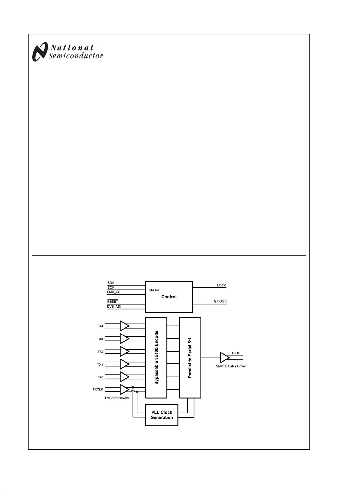
The LMH0340 3 Gbps SDI Serializer is part of National’s family of FPGA-Attach SER/DES products supporting 5-bit LVDS
interfaces with FPGAs. An FPGA Host will format data with
supplied IP such that the output of the LMH0340 is compliant
with the requirements of DVB-ASI, SMPTE 259M-C, SMPTE
292M and SMPTE 424M standards.
The interface between the SER (Serializer) and the FPGA
consists of a 5 bit wide LVDS data bus, an LVDS clock and
an SMBus interface. The LMH0340 / LMH0040 / LMH0070
SER devices include an integrated cable driver which is fully
compliant with all of the SMPTE specifications listed above.
Refer to Table 1 for a complete listing of single channel serializers currently offered in this family. The LMH0050 has a
CML output driver that can drive a differential transmission
line or interface to a cable driver.
The FPGA-Attach SER/DES family is supported by a suite of
IP which allows the design engineer to quickly develop video
applications using the SER/DES products. The SER is packaged in a physically small 48 pin LLP package.
Key Specifications
■
Output compliant with SMPTE 424M, SMPTE 292M,
SMPTE 259M-C and DVB-ASI
■
Typical power dissipation: 440 mW
■
30 ps typical output jitter (HD, 3G)
Features
■
LVDS Interface to Host FPGA
■
No external VCO or clock ref required
■
Integrated Variable Output Cable Driver
■
3.3V SMBus configuration interface
■
Integrated TXCLK PLL cleans clock noise
■
Small 48pin LLP package
Applications
■
SDI interfaces for:
—
Video Cameras
—
DVRs
—
Video Switchers
—
Video Editing Systems
General Block Diagram
30017001
TRI-STATE® is a registered trademark of National Semiconductor Corporation.
© 2008 National Semiconductor Corporation 300170 www.national.com
LMH0340, LMH0040, LMH0070, LMH0050 3Gbps, HD, SD, DVB-ASI SDI Serializer and Cable
Driver with LVDS Interface
Page 2
Pin Descriptions
Pin Name Type Description
LVDS Input Interface
TX[4:0]+
TX[4:0]-
Input, LVDS LVDS Data Input Pins
Five channel wide DDR interface. Internal 100Ω termination.
TXCLK+
TXCLK-
Input, LVDS LVDS Clock Input Pins
DDR Interface. Internal 100Ω termination.
Serial Output Interface
TXOUT+ Output, CML Serial Digital Interface Output Pin
Non-Inverting Output
TXOUT- Output, CML Serial Digital Interface Output Pin
Inverting Output
SMBus Interface
SDA I/O, LVCMOS SMBus Data I/O Pin
SCK Input, LVCMOS SMBus Clock Input Pin
SMB_CS Input, LVCMOS SMBus Chip Select Input Pin
Device is selected when High.
Control and Configuration Pins
RESET Input, LVCMOS Reset Input Pin
H = normal mode
L = device in RESET
LOCK Output, LVCMOS PLL LOCK Status Output
H = unlock condition
L = Device is Locked
DVB_ASI Input, LVCMOS DVB_ASI Select Input
H = DVB_ASI Mode enabled
L = Normal Mode enabled
GPIO[2:0] I/O, LVCMOS General Purpose Input / Output
Software configurable I/O pins.
RSVD_H Input, LVCMOS Configuration Input – Must tie High
Pull High via 5 kΩ resistor to V
DD3V3
Analog Inputs
R
SET
Input, analog Serial Output Amplitude Control
Resistor connected from this pin to ground to set the signal amplitude. Nominally
8.06kΩ for 800mV output (SMPTE).
LF_CP Input, analog Loop Filter Connection
LF_REF Input, analog Loop Filter Reference
DNC Do Not Connect – Leave Open
Power Supply and Ground
V
DD3V3
Power 3.3V Power Supply connection
V
DDPLL
Power 3.3V PLL Power Supply connection
V
DD2V5
Power 2.5V Power Supply connection
GND Ground Ground connection – The DAP (large center pad) is the primary GND connection
for the device and must be connected to Ground along with the GND pins.
TABLE 1. Feature Table
Device
SMPTE 424M
Support (3G)
SMPTE 292M
Support (HD)
SMPTE 259M
Support (SD)
DVB-ASI
Support
SMPTE compliant
Cable Driver
LMH0340 X X X X X
LMH0040 X X X X
LMH0070 X X X
LMH0050 X X X
www.national.com 2
LMH0340, LMH0040, LMH0070, LMH0050
Page 3
Absolute Maximum Ratings (Note 1)
If Military/Aerospace specified devices are required,
please contact the National Semiconductor Sales Office/
Distributors for availability and specifications.
Supply Voltage (V
DD3V3
) −0.3V to +4.0V
Supply Voltage (V
DD2V5
) −0.3V to +3.0V
LVCMOS input voltage −0.3V to (V
DD3V3
+0.3V)
LVCMOS output voltage −0.3V to (V
DD3V3
+0.3V)
SMBus I/O voltage -0.3V to +3.6V
LVDS Input Voltage -0.3V to +3.6V
Junction Temperature +150°C
Storage Temperature −65° to 150°C
Thermal Resistance—
Junction to Ambient—θ
JA
25°C/W
ESD Rating—Human Body Model,
1.5 KΩ, 100 pF
≥±8kV
Recommended Operating Conditions
Parameter Min Typ Max Units
Supply Voltage (V
DD3V3
-GND) 3.135 3.3 3.465 V
Supply Voltage (V
DD2V5
-GND) 2.375 2.5 2.625 V
Supply noise amplitude (10 Hz to 50 MHz) 100 mV
P-P
Ambient Temperature −40 +25 +85 °C
Case Temperature 100 °C
TXCLK input frequency – LMH0340 27 297 MHz
TXCLK input frequency – LMH0040 27 149 MHz
TXCLK input frequency – LMH0070 26.5 27 28 MHz
TXCLK input frequency – LMH0050 27 149 MHz
LVDS PCB board trace length (mismatch <2%) 25 cm
Output Driver Pullup Resistor Termination Voltage (Note 10) 2.5 2.625 V
Electrical Characteristics
Over supply and Operating Temperature ranges unless otherwise specified. (Note 2)
Symbol Parameter Condition Min Typ Max Units
I
DD2.5
2.5V supply current for LMH0340,
LMH0040, or LMH0070
2.97 Gbps 93 102 mA
1.485 Gbps 80 87 mA
270 Mbps 63 69 mA
2.5V supply current for LMH0050 1.485 Gbps 87 95 mA
270 Mbps 70 75 mA
I
DD3.3
3.3V supply current for LMH0340,
LMH0040, or LMH0070
2.97 Gbps 73 85 mA
1.485 Gbps 73 85 mA
270 Mbps 73 85 mA
3.3V supply current for LMH0050 1.485 Gbps 73 85 mA
270 Mbps 73 85 mA
PD Power Consumption LMH0340 - 2.97 Gbps 475 545 mW
LMH0040 - 1.485 Gbps 440 510 mW
LMH0050 - 1.485 Gbps 460 525 mW
LMH0050 - 270 Mbps 415 485 mW
LMH0070 - 270 Mbps 400 470 mW
Control Pin Electrical Characteristics
Over supply and Operating Temperature ranges unless otherwise specified. Applies to DVB_ASI, RESET
, GPIO[2:0] and LOCK.
(Note 2)
Symbol Parameter Condition Min Typ Max Units
V
IH
High Level Input Voltage 2.0 V
DD3V3
V
V
IL
Low Level Input Voltage 0 0.8 V
V
OH
High Level Output Voltage IOH=−2 mA 2.7 3.3 V
V
OL
Low Level Output Voltage IOL=2 mA 0.3 V
V
CL
Input Clamp Voltage ICL=−18 mA -0.79 -1.5 V
3 www.national.com
LMH0340, LMH0040, LMH0070, LMH0050
Page 4
Symbol Parameter Condition Min Typ Max Units
I
IN
Input Current VIN=0.4V, 2.5V or V
DD
-35 35
μA
I
OS
Output Short Circuit Current V
OUT
=0V -40 mA
LVDS Input Electrical Characteristics
Over supply and Operating Temperature ranges unless otherwise specified. (Note 2)
Symbol Parameter Condition Min Typ Max Units
V
TH
Differential Input High threshold 0.05V<VCM<2.4V +100 mV
V
TL
Differential Input Low threshold −100 mV
R
LVIN
Input Impedance Measured between LVDS pairs 85 100 115
Ω
LVDS Switching Characteristics
Over supply and Operating Temperature ranges unless otherwise specified. (Note 2)
Symbol Parameter Condition Min Typ Max Units
t
CIP
TxCLKIN Period See Figure 1 3.2 2T 37 ns
t
CIT
TxCLKIN Transition Time See Figure 2 0.5 1.0 3.0 ns
t
CIH
TxCLKIN IN High Time See Figure 1 0.7T T 1.3T ns
t
CIL
TxCLKIN IN Low Time See Figure 1 0.7T T 1.3T ns
t
XIT
TxIN Transition Time 0.15 3 ns
t
STC
TxIN Setup to TxCLKIN See Figure 1, (Note 11) -550 ps
t
HTC
TxIN Hold to TxCLKIN 900 ps
30017002
FIGURE 1. LVDS Input Timing Diagram
30017003
FIGURE 2. Transmit Clock Transition Times
www.national.com 4
LMH0340, LMH0040, LMH0070, LMH0050
Page 5
SMBus Input Electrical Characteristics
Over supply and Operating Temperature ranges unless otherwise specified. (Note 2)
Symbol Parameter Condition Min Typ Max Units
V
SIL
Data, Clock Input Low Voltage 0.8 V
V
SIH
Data, Clock Input High Voltage 2 V
SDD
V
I
SPULLUP
Current through pull-up resistor or
current source
(Note 3) 4 mA
V
SDD
Nominal Bus Voltage 2.375 3.6 V
I
SLEAKB
Input Leakage per bus segment (Note 3) −200 200
μA
I
SLEAKP
Input Leakage per pin −10 10
μA
C
SI
Capacitance for SMBdata and
SMBclk
(Notes 3, 4) 10 pF
R
STERM
Termination Resistance V
SDD3V3
(Notes 5, 4, 3) 1000
Ω
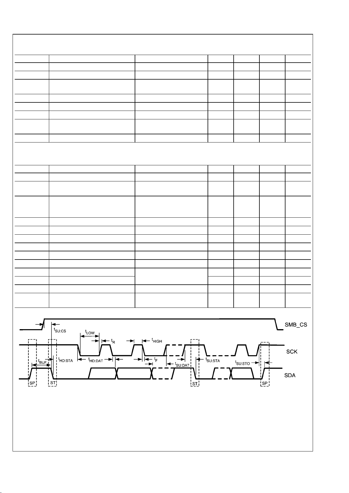
SMBus Switching Characteristics
Over supply and Operating Temperature ranges unless otherwise specified. (Note 2)
Symbol Parameter Condition Min Typ Max Units
f
SMB
Bus Operating Frequency 10 100 kHz
t
BUF
Bus free time between stop and start
condition
4.7
μs
t
HD:STA
Hold time after (repeated) start
condition. After this period, the first
clock is generated
At I
SPULLUP
= MAX 4.0
μs
t
SU:STA
Repeated Start condition setup time 4.7
μs
t
SU:STO
Stop Condition setup time 4.0
μs
t
HD:DAT
Data hold time 300 ns
t
SU:DAT
Data setup time 250 ns
t
LOW
Clock Low Time 4.7
μs
t
HIGH
Clock High Time 4.0 50
μs
t
F
Clock/data fall time 20% to 80% 300 ns
t
R
Clock/data rise time 1000 ns
t
SU:CS
SMB_CS setup time 30 ns
t
POR
Time in which a device must be
operational after power on
500 ms
30017004
(levels are V
SIL
and V
SIH
)
FIGURE 3. SMBus Timing Parameters
5 www.national.com
LMH0340, LMH0040, LMH0070, LMH0050
Page 6
SDI Output Characteristics — LMH0340 / LMH0040 / LMH0070
Over supply and Operating Temperature ranges unless otherwise specified. (Note 2)
Symbol Parameter Condition Min Typ Max Units
V
OD
SDI Output Voltage
into 75Ω load
720 800 880 mV
DR SDI Output Datarate LMH0340 270 2,970 Mbps
LMH0040 270 1,485 Mbps
LMH0070 270 Mbps
t
r
SDI Output Rise Time 2.97 Gbps 90 135 ps
1.485 Gbps 90 220 ps
<1.485 Gbps 400 700 1000 ps
t
f
SDI Output Fall Time 2.97 Gbps 90 135 ps
1.485 Gbps 90 220 ps
<1.485 Gbps 400 700 1000 ps
Δt
t
Mismatch between rise and fall time
≥1.485 Gbps
(Note 9)
30 ps
t
SD
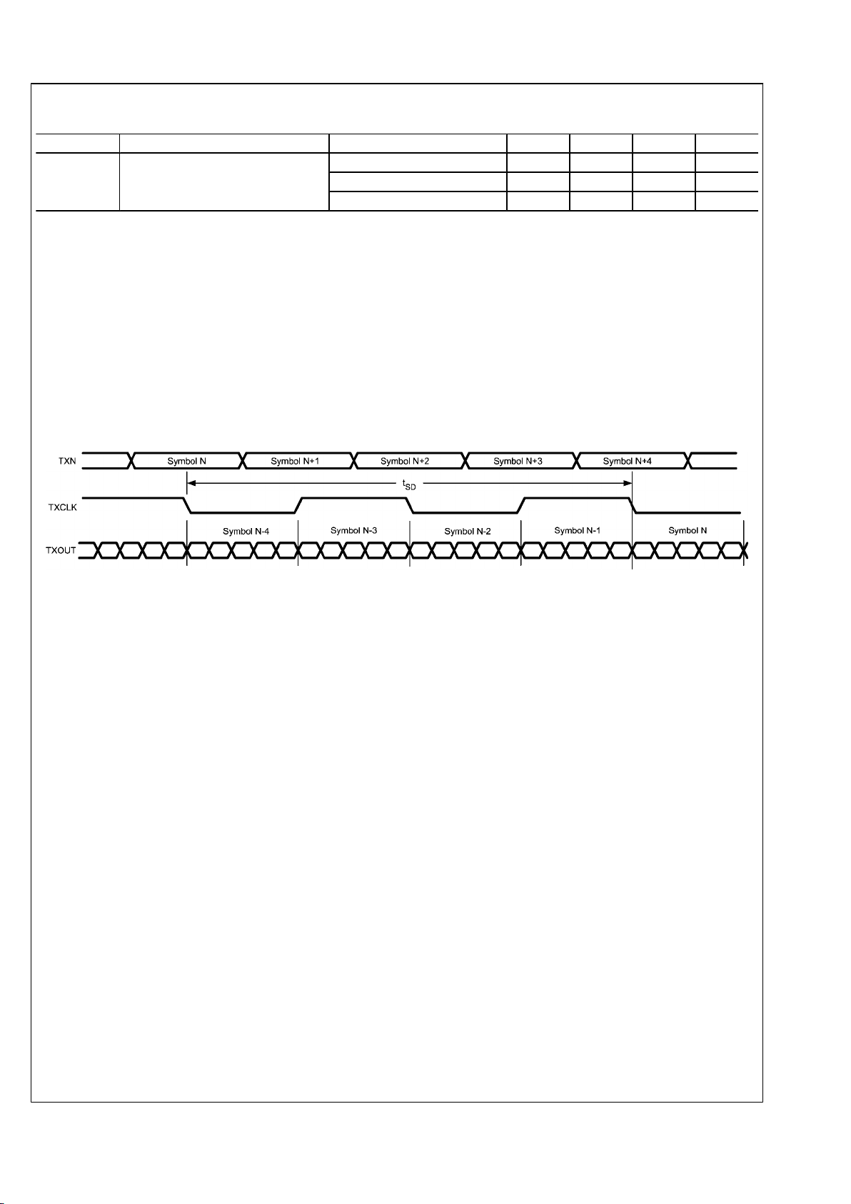
Propagation Delay Latency See Figure 4 9.5 TXCLK
cycle
t
J
Peak to Peak Alignment Jitter
≥1.485 Gbps(Note 6)
30 50 ps
270 Mbps(Note 6) 100 200 ps
RL Output Return Loss — EVK
Specification
(Note 12)
Measured 5 MHz to 1485 MHz 15 20 dB
Measured 1485 MHz to 2970
MHz
10 15 dB
t
OS
Output Overshoot
(Note 9)
2.97 Gbps 8 %
1.485 Gbps 5 %
270 Mbps 2 %
CML Output Characteristics — LMH0050
Over supply and Operating Temperature ranges unless otherwise specified. (Note 2)
Symbol Parameter Condition Min Typ Max Units
V
OD
Output Voltage
into 100 Ω differential load
1175 1450 mV
DR Data Rate 270 1485 Mbps
t
r
Output Rise Time 100 ps
t
f
Output Fall Time 100 ps
t
J
Peak-to-Peak Alignment Jitter 1.485 Gbps 25 50 ps
R
OUT
Output Termination Resistance Output Pin to V
DD2V5
Pin 40 50 60
Ω
www.national.com 6
LMH0340, LMH0040, LMH0070, LMH0050
Page 7
Device Switching Characteristics
Over supply and Operating Temperature ranges unless otherwise specified. (Note 2)
Symbol Parameter Condition Min Typ Max Units
t
TPLD
Device Lock Time 2.97 Gbps 10 ms
1.485 Gbps 11 ms
270 Mbps 15 ms
Note 1: “Absolute Maximum Ratings” are limits beyond which the safety of the device cannot be guaranteed. It is not implied that the device will operate up to
these limits.
Note 2: Typical Parameters measured at V
DD3V3
=3.3V, V
DD2V5
=2.5V, TA=25°C. They are for reference purposes and are not production tested.
Note 3: Recommended value—Parameter is not tested.
Note 4: Recommended maximum capacitance load per bus segment is 400 pF.
Note 5: Maximum termination voltage should be identical to the device supply voltage.
Note 6: Measured in accordance with SMPTE RP184. 100% production tested.
Note 7: Register 0x30'h bits [7:5] is at default value of 011'b
Note 8: Measured with R
SET
= 8.06 kΩ and register 0x69'h at default value.
Note 9: Specification guaranteed by characterization.
Note 10: Applies to LMH0340, LMH0040, and LMH0070.
Note 11: Parameter uses default settings in registers: 0x24'h and 0x30'h.
Note 12: Output Return Loss specification applies to measurement on the EVK PCB (LMH0340 ALP Daughter Card) per SMPTE requirements.
30017005
FIGURE 4. LVDS Interface Propagation Delay
7 www.national.com
LMH0340, LMH0040, LMH0070, LMH0050
Page 8

Functional Description
DEVICE OPERATION
The SER is used in digital video signal origination equipment.
It is intended to be operated in conjunction with an FPGA host
which preprocesses data for it, and then provides this data
over the five bit wide data path. Provided the host has properly
formatted the data for the SER, the output of the device will
be compliant with DVB-ASI, SMPTE 259M-C, SMPTE 292M
or SMPTE 424M depending upon the output mode selected.
National Semiconductor offers IP in source code format to
perform the appropriate formatting of the data, as well as
evaluation platforms to assist in the development of target
applications. For more information please contact your local
National Semiconductor Sales Office/Distributor.
POWER SUPPLIES
The SER has several power supply pins, at 2.5V as well as
3.3V. It is important that these pins all be connected, and
properly bypassed. Bypassing should consist of parallel
4.7μF and 0.1μF capacitors as a minimum, with a 0.1μF capacitor on each power pin. The device has a large contact in
the center of the bottom of the package. This contact must be
connected to the system GND as it is the major ground connection for the device. A 22 μF capacitor is required on the
V
DDPLL
pin which is connected to the 3.3V rail.
Discrete bypassing is ineffective above 30 MHz to 50 MHz in
power plane-based distribution systems. Above this frequency range, the intrinsic capacitance of the power-ground system can be used to provide additional RF bypassing. To make
the best use of this, make certain that there are PCB layers
dedicated to the Power supplies and to GND, and that they
are placed next to each other to provide a distributed capacitance between power and GND.
The SER will work best when powered from linear regulators.
The output of linear regulators is generally cleaner with less
noise than switching regulators. Output filtering and power
system frequency compensation are generally simpler and
more effective with linear regulators. Low dropout linear regulators are available which can usually operate from lower
input voltages such as logic power supplies, thereby reducing
regulator power dissipation. Cascading of low dropout regulators should not be done since this places the entire supply
current load of both load systems on the first regulator in the
cascade and increases its loading and thermal output.
POWER UP
The 3.3V power supply should be brought up before the 2.5V
supply. The timing of the supply sequencing is not important.
The device has a power on reset sequence which takes place
once both power supplies are brought up. This sequence will
reset all register contents to their default values, and will place
the PLLs into link acquisition mode, attempting to lock on the
TXCLK input.
RESET
There are three ways in which the device may be reset. There
is an automatic reset which happens on power-up; there is a
reset pin, which when brought low will reset the device, with
normal operation resuming when the pin is driven high again.
The third way to reset the device is a soft reset, implemented
via a write to the reset register. This reset will put all of the
register values back to their default values, except it will not
affect the address register value if the SMBus default address
has been changed.
LVDS INPUTS
The SER has LVDS inputs that conform with the ANSI/TIA/
EIA-644–A Standard. These inputs have an internal 100 Ω
resistor across the inputs which allows for the closing of a
current loop interface from the LVDS driver in the host. It is
recommended that the PCB trace between the FPGA and the
transmitter be less than 25cm. Longer PCB traces may introduce signal degradation as well as channel skew which could
cause serialization errors. This connection between the host
and the SER should be over a controlled impedance transmission line with an impedance which matches the termination resistor – usually 100 Ω. Setup and hold times are
specified in the LVDS Switching Characteristics table, however there is the ability to change these by use of the CLK
delay adjustment available via the SMBus, and writing to register 0x30'h.
LVDS DATA ORDER
When serializing the data, the data bit latched in on TX0 is
output first, followed by TX1, TX2, TX3 and then TX4. If starting with a 10 bit word, T0..T9, with T0 being the LSB, and it
is desired that this be serialized such that the LSB is sent out
first, then the least significant 5 bit word would be provided to
the serializer first, followed by the most significant word, and
the resulting serialized output would have the LSB being sent
first, and the 10 bit MSB (T9) would be transmitted last. If it is
desired to reverse the serialization order, such that the bit
presented on TX4 is output first, this mode of operation may
be selected via register 0x2E'h.
LOOP FILTER
The SER has an internal PLL which is used to generate the
serialization clock from the parallel clock input. The loop filter
for this PLL is external, and for optimum results in Serial Digital Interface applications, a capacitor and a resistor in series
should be connected between pins 26 and 27. Recommended value for the capacitor is 0.1 μF. Recommended value for
the resistor is 500 Ω.
PLL FILTER / BYPASS
The SER has an external filter capacitor for the PLL. The recommended value for this capacitor is 22 μF with a connection
to the 3.3V rail.
DVB_ASI MODE
The SER has a special mode for DVB-ASI. In this mode, the
input signal on TX4± is treated as a data valid bit, if high, then
the four bit nibbles from TX0-TX3 are taken to form an 8 bit
word, which is then converted to a 10 bit code via an internal
8b10b encoder and this 10 bit word is serialized and driven
on the output. The nibble taken in on the rising edge of the
clock is the most significant nibble and the nibble taken in on
the falling edge is the least significant nibble. If TX4± is low,
then the input on TX0-TX3 are ignored and the 10b idle character is inserted in the output stream. The Idle character can
be reprogrammed to be any 10 bit code desired via registers
0x11'h and 0x12'h.
SDI OUTPUT INTERFACING
The serial outputs provide low-skew complimentary or differential signals. The output buffer is a current mode design, with
a high impedance output. To drive a 75Ω transmission line
connect a 75Ω resistor from each of the output pins to 2.5V.
This resistor has two functions – it converts the current output
to a voltage, which is used to drive the cable, and it acts as
the back termination resistor for the transmission line. The
resistor should be placed as close to the output pin as is
www.national.com 8
LMH0340, LMH0040, LMH0070, LMH0050
Page 9

practicable. The output driver automatically adjusts its slew
rate depending on the input datarate so that it will be in compliance with SMPTE 259M, SMPTE292M or SMPTE 424M as
appropriate. In addition to output amplitude and rise/fall time
specifications, the SMPTE specs require that SDI outputs
meet an Output Return Loss (ORL) specification. There are
parasitic capacitances that will be present both at the output
pin of the device and on the application printed circuit board.
To optimize the return loss implement a series network comprised of a parallel inductor and resistor. The actual values for
these components will vary from application to application,
but the typical interface circuit shows values that would be a
good starting point. Figure 5 shows an equivalent output circuit for the LMH0340 / LMH0040 / LMH0070. The collectors
present a high impedance current source. The external 75Ω
resistors will provide the back termination resistance as well
as converting the current to a voltage – with the addition of
the termination resistance at the load, there will be an overall
output resistance of 37.5Ω, which in conjunction with the 24mA current source will develop the 800mV swings called for
in the standard.
30017007
FIGURE 5. Simplified SDI Output Circuit
Care must be taken in the layout of the output circuitry to meet
SMPTE return loss specifications as any parasitic
impedances or transmission line discontinuities will result in
reflections which will adversely affect the output return loss.
For more details on how to get good output return loss, please
refer to the application note “Successful design with the
FPGA-Attach SER/DES”.
30017011
FIGURE 6. SDI Output Return Loss (EVK Example)
The amplitude of the output is guaranteed to be compliant with
SMPTE specifications if the specified value of R
SET
resistor is
used, however if the designer wishes to change the output
amplitude, there are two methods by which this can be done.
By changing the value of resistor connected to the R
SET
pin,
the output amplitude will be adjusted.
30017012
FIGURE 7. Output Voltage vs. R
SET
9 www.national.com
LMH0340, LMH0040, LMH0070, LMH0050
Page 10

CML Output Interfacing
The LMH0050 does not include the internal SMPTE cable
driver, as its outputs are CML, include internal 50 Ω pull up
resistors, and are intended to drive 100 Ω transmission lines.
The LMH0050 outputs may either be connected to a differential transmission medium such as twisted pair cable, or
used to drive an external cable driver.
Power Down Mode
If the device is not to be used, some power can be saved by
writing a ‘0x40h’ to register 0x26'h, and a 0x10'h to register
0x01'h. The write to register 0x26'h will disable the input
buffers of the device, and the write to register 0x01'h will power down the output buffer. In this mode, the device power
dissipation can be expected to be reduced by approximately
30%. There are portions of the circuit which will automatically
power down if there is no clock present on the TXCLK input,
so this method can be used to further reduce the power.
SMBus INTERFACE
The configuration bus conforms to the System Management
Bus (SMBus) 2.0 specification. SMBus 2.0 includes multiple
options. The optional ARP (Address Resolution Protocol) feature is not supported. The I/O rail is 3.3V only and is not 5V
tolerant. The use of the SMB_CS signal is recommended for
applications with multi-drop applications (multiple devices to
a host).
The SMBus is a two wire interface designed for the communication between various system component chips, additional
signals maybe required for chip select function depending
upon application. By accessing the control functions of the
circuit via the SMBus, signal count is kept to a minimum while
allowing a maximum amount of versatility. The SMBus has
three pins to control it: an SMBus CS pin which enables the
SMBus interface for the device, a Clock and a Data line. In
applications where there might be several SER devices, the
SDA and SCK pins can be bussed together and the individual
devices to be communicated with may be selected via their
respective SMB_CS pin. The SCK and SDA are both open
drain and are pulled high by external pullup resistors. The
SER has several internal configuration registers which may
be accessed via the SMBus. These registers are listed in SER
Register Detail Table.
TRANSFER OF DATA TO THE DEVICE VIA THE SMBus
During normal operation the data on SDA must be stable dur-
ing the time when SCK is high.
START / STOP / IDLE CONDITIONS
There are three unique states for the SMBus:
START A HIGH-to-LOW transition on SDA while SCK is
High indicates a message START condition
STOP A LOW-to-HIGH transition on SDA while SCK is
High indicates a message STOP condition.
IDLE If SCK and SDA are both High for a time exceeding
t
BUF
from the last detected STOP condition or if they
are high for a total exceeding the maximum
specification for t
HIGH
then the bus will transfer to the
IDLE state.
SMBus TRANSACTIONS
A transaction begins with the host placing the SER SMBus
into the START condition. Then a byte (8 bits) is transferred,
MSB first, followed by a ninth ACK bit. ACK bits are ‘0’ to signify an ACK, or ‘1’ to signify NACK. After this the host holds
the SCK line Low, and waits for the receiver to raise the SDA
line as an ACKnowledge that the byte has been received.
REGISTER WRITE
To write a data value to a register in the SER, the host writes
three bytes to the SER. The first byte is the device address—
the device address is a 7 bit value, and if writing to the SER
the last bit (LSB) is set to ‘0’ to signify that the operation is a
write. The second byte written is the register address, and the
third byte written is the data to be written into the addressed
register. If additional data writes are performed, the register
address is automatically incremented. At the end of the write
cycle the host places the bus in the STOP state.
REGISTER READ
To read the data value from a register, first the host writes the
device address with the LSB set to a ‘0’ denoting a write, and
then the register address is written to the device. The host
then reasserts the START condition, and writes the device
address once again, but this time with the LSB set to a ‘1’
denoting a read, and following this the SER will drive the SDA
line with the data from the addressed register. The host indicates that it has finished reading the data by asserting a ‘0’
for the ACK bit. After reading the last byte, the host will assert
a ‘1’ for NACK to indicate to the SER that it does not require
any more data.
Note that the SMBus pins are not 5V compliant and they
must be driven by a 3.3V source.
SMBus CONFIGURATIONS
Many different configurations of the SMBus are possible and
depend upon the specific requirements of the applications.
Several possible applications are described.
CONFIGURATION 1
The SER SMB_CS may be tied High (always enabled) since
it is the only device on the SMBus. See Figure 8.
CONFIGURATION 2
Since the multiple SER devices have the same address, the
use of the individual SMB_CS signals is required. To communicate with a specific device, its SMB_CS is driven High to
select the device. After the transaction is complete, its
SMB_CS is driven Low to disable its SMB interface. Other
devices on the bus may now be selected with their respective
chip select signals and communicated with. See Figure 9.
CONFIGURATION 3
The addressing field is limited to 7-bits by the SMBus protocol.
Thus it is possible that multiple devices may share the same
7-bit address. An optional feature in the SMBus 2.0 specification supports an Address Resolution Protocol (ARP). This
optional feature is not supported by the
LMH0340/0040/0070/0050 devices. Solutions for this include: the use of the independent SMB_CS signals, independent SMBus segments, or other means. See Figure 10.
www.national.com 10
LMH0340, LMH0040, LMH0070, LMH0050
Page 11

30017015
FIGURE 8. SMBus Configuration 1 — Host to single device
30017016
FIGURE 9. SMBus Configuration 2 — Host to multiple devices with SMB_CS signals
30017017
FIGURE 10. SMBus Configuration 3 — Host to multiple devices with multiple SMBus Interfaces
11 www.national.com
LMH0340, LMH0040, LMH0070, LMH0050
Page 12

GENERAL PURPOSE I/O PINS GPIO[2:0]
The SER has three pins which can be configured to provide
direct access to certain register values via a dedicated pin.
For example if a particular application required fast action to
the condition of the serializer losing it’s input clock, the TXCLK
detect status bit could be routed directly to an external pin
where it might generate an interrupt for the host processor.
GPIO pins can be configured to be in TRI-STATE®(High
Impedance) mode, the buffers can be disabled, and when
used as inputs can be configured with a pullup resistor, a
pulldown resistor or no input pin biasing at all. When the GPIO
pins are being used as inputs, there is the ability to have an
internal pullup or pull down resistor. This is selected via the
GPIO Configuration registers.
Each of the GPIO pins has a register to control it. For each of
these registers, the upper 4 bits are used to define what function is desired of the GPIO pin with options being slightly
different for each of the three GPIO pins. The pins can be
used to monitor the status of various internal states of the SER
device, to serve as an input from some external stimulus, and
for output to control some external function.
GPIO_0 FUNCTIONS
Allow for the output of a signal programmed by the SMBus
Allow the monitoring of an external signal via the SMBus
Monitor Status of TXCLK signal
Monitor Status of TXCLKDetect
Monitor Power On Reset
GPIO_1 FUNCTIONS
Monitor Power On Reset
Allow for the output of a signal programmed by the SMBus
Allow the monitoring of an external signal via the SMBus
Monitor LOS for data bit 0
Monitor LOS for data bit 1
Monitor LOS for data bit 2
Monitor LOS for data bit 3
Monitor LOS for data bit 4
GPIO_2 FUNCTIONS
Allow for the output of a signal programmed by the SMBus
Allow the monitoring of an external signal via the SMBus
Serializer Clock output
Bits 2 and 3 are used to determine the status of the internal
pullup/pulldown resistors on the device—they are loaded according to the following truth table:
00: pullup and pulldown disabled
01: pulldown enabled
10: pullup enabled
11: Reserved
Bit 1 is used to enable or disable the input buffer. If the GPIO
pin is to be used as an output pin, then this bit must be set to
a ‘0’ disabling the output.
The LSB is used to switch the output between normal output
state and high impedance mode. If the GPIO is to be used as
an input pin, this bit must be set to ‘0’ placing the output in
high Z mode.
As an example, if you wanted to use the GPIO0 pin to reflect
the status of the LOCK pin, you would load the appropriate
register with the value 0001 0001b.
POTENTIAL APPLICATION FOR GPIO PINS
In addition to being useful debug tools while bringing a design
up, there are other practical uses to which the GPIO pins can
be put:
Sensing if a cable is connected to an output –
When connecting the BNC cable to the output, connect the
shield of the connector to GND via a capacitor—making it an
AC GND, but a DC open. Now connect that shield to one of
the GPIO connections which you configure as an input with a
pullup. With no cable on the BNC, the GPIO pin will see a high
state, but once a terminated cable is connected, the shield will
be brought down and you will read a low state.
30017008
FIGURE 11. Simplified LVCMOS Input Circuit
30017009
FIGURE 12. Simplified LVCMOS Output Circuit
www.national.com 12
LMH0340, LMH0040, LMH0070, LMH0050
Page 13

Application Information
PCB RECOMMENDATIONS
The SMPTE Serial specifications have very stringent requirements for output return loss on drivers. The output return loss
will be degraded by non-idealities in the connection between
the SER (all variants with the exception of the LMH0050) and
the output connector. All efforts should be taken to minimize
the trace lengths for this area, and to assure that the characteristic impedance of this trace is 75Ω.
It is recommended that the PCB traces between the host FPGA and the SER be no longer than 10 inches (25cm) and that
the traces be routed as differential pairs, with very tight matching of line lengths and coupling within a pair, as well as equal
length traces for each of the six pairs. For additional information on layout and soldering of the LLP package, please refer
to the applications note 'AN 1187'
PCB Design do’s and don’ts:
•
DO Whenever possible dedicate an entire layer to each
power supply – this will reduce the inductance in the
supply plane.
•
DO use surface mount components whenever possible
•
DO place bypass capacitors close to each power pin
•
DON’T create ground loops – pay attention to the cutouts
that are made in your power and ground planes to make
sure that there are not opportunities for loops.
•
DON’T allow discontinuities in the ground planes – return
currents will follow the path of least resistance – for high
frequency signals this will be the path of least inductance.
•
DO place the SER outputs as close as possible to the edge
of the PCB where it will connect to the outside world.
•
DO make sure to match the trace lengths of all differential
traces, both between the sides of an individual pair, and
from pair to pair.
•
DO remember that VIAs have significant inductance –
when using a via to connect to a power supply or ground
layer, two in parallel are better than one.
•
DO connect the slug on the bottom of the package to a
solid Ground connection. This contact is used for the major
GND connection to the device as well as serving as a
thermal via to keep the die at a low operating temperature.
•
There is an application note available which discusses
layout suggestions for the SER in greater detail.
TYPICAL SMPTE APPLICATIONS CIRCUIT
A typical application circuit for the LMH0340 is shown in Figure 13. Alternately this could also employ the LMH0040 or
LMH0070 Serializers in lower data rate SMPTE applications.
The TX interface between the host FPGA and the SER is
composed of a 5-bit LVDS Data bus and its LVDS clock. This
is a point-to-point interface and the SER includes on-chip 100
terminations. Pairs should be of equal length to minimize any
skew impact. The LVDS clock (TXCLK) uses both edges to
transfer the data.
An SMBus is also connected from the host FPGA to the SER.
If the SMBus is shared, a chip select signal is used to select
the device being addressed. The SCK and SDA signals require a pull up resistor. The SMB_CS is driven by a GPO
signal from the FPGA. Depending on the FPGA I/O it may also
require a pull up unless it is a push / pull output.
Depending upon the application, several other GPIO signals
maybe used. This includes the DVB_ASI and RESET input
signals. If these pins are not used, then must be tied off to the
desired state. The LOCK signal maybe used to monitor the
SER. If it is unused, leave the pin as a NC (or route to a test
point).
The SER includes a SMPTE compliant cable driver. While this
is a differential driver, it is commonly used single-endedly to
drive 75 Ω coax cables. External 75 Ω pull up resistors are
used to the 2.5V rail. The active output(s) also includes a
matching network to meet the required Output Return Loss
SMPTE specification. While application specific, in general a
series 75 Ω resistor shunted by a 6.8 nH inductor will provide
a starting value to design with. The signal is then AC coupled
to the cable with a 4.7 µF capacitor. If the complementary
output is not used, simply terminate it after its AC coupling
capacitor to ground. This output (even though its inverting)
may still be used for a loop back or 1:2 function due to the
nature of the NRZI coding that the SMPTE standards require.
The output voltage amplitude of the cable driver is set by the
R
SET
resistor. For single-ended applications, an 8.06 kΩ re-
sistor is connected between this pin and ground to set the
swing to 800mV.
The PLL loop filter is external for the SER. A capacitor is connected in series to a resistor between the LF_CP and LF_REF
pins. Typical values are 500 Ω and 0.1 µF.
There are several configuration pins that requiring setting to
the proper level. The RSVD_H pins should be pulled High to
the 3.3V rail with a 5 kΩ resistor. Depending upon the application the DVB_ASI pin may be tied off or driven.
There are three supply connections (see By Pass discussion
and also Pin Descriptions for recommendations). The two
main supplies are the 3.3V rail and the 2.5V rail. There is also
a 3.3V connection for the PLL circuitry.
There are multiple Ground connections for the device. The
main ground connection for the SER is through the large center DAP pad. This must be connected to ground for proper
device operation. In addition, multiple other inputs are required to be connected to ground as show in the figure and
listed in the Pin Description table.
13 www.national.com
LMH0340, LMH0040, LMH0070, LMH0050
Page 14

30017006
FIGURE 13. Typical SMPTE Application Circuit
TYPICAL LMH0050 CML APPLICATIONS CIRCUIT
A typical application circuit for the LMH0050 is shown in Figure 14.
The TX interface between the host FPGA and the SER is
composed of a 5-bit LVDS Data bus and its LVDS clock. This
is a point-to-point interface and the SER includes on-chip 100
terminations. Pairs should be of equal length to minimize any
skew impact. The LVDS clock (TXCLK) uses both edges to
transfer the data.
An SMBus is also connected from the host FPGA to the SER.
If the SMBus is shared, a chip select signal is used to select
the device being addressed. The SCLK and SDA signals require a pull up resistor. The SMB_CS is driven by a GPO
signal from the FPGA. Depending on the FPGA I/O it may also
require a pull up unless it is a push / pull output.
Depending upon the application, several other GPIO signals
maybe used. This includes the DVB_ASI and RESET input
signals. If these pins are not used, then must be tied off to the
desired state. The LOCK signal maybe used to monitor the
SER. If it is unused, leave the pin as a NC (or route to a test
point).
The LMH0050 SER includes a CML cable driver. This is a
differential driver, and includes internal 50 Ω pull up resistors
to the 2.5V rail. The output voltage amplitude of the cable
driver is set by the R
SET
resistor. The R
SET
resistor recom-
mended value for the LMH0050 is 9.1KΩ. It is intended to
drive 100 Ω differential pairs or twisted pair cables.
The PLL loop filter is external for the SER. A capacitor is connected in series to a resistor between the LF_CP and LF_REF
pins. Typical values are 500 Ω and 0.1 µF.
There are several configuration pins that requiring setting to
the proper level. The RSVD_H pins should be pulled High to
the 3.3V rail with a 5 kΩ resistor. Depending upon the application the DVB_ASI pin may be tied off or driven.
There are three supply connections (see By Pass discussion
and also Pin Descriptions for recommendations). The two
main supplies are the 3.3V rail and the 2.5V rail. There is also
a 3.3V connection for the PLL circuitry.
There are multiple Ground connections for the device. The
main ground connection for the SER is through the large center DAP pad. This must be connected to ground for proper
device operation. In addition, multiple other inputs are required to be connected to ground as show in the figure and
listed in the Pin Description table.
www.national.com 14
LMH0340, LMH0040, LMH0070, LMH0050
Page 15

30017013
FIGURE 14. Typical LMH0050 CML Application Circuit
SERIAL JITTER OPTIMIZATION
The SER is capable of very low jitter operation, however it is
dependent on the TXCLK provided by the host in order to operate, and depending on the quality of the TXCLK provided,
the SER output jitter may not be as low as it could be.
The SER includes circuitry to filter out any TXCLK jitter at frequencies above 1MHz (see Figure 15), however, for frequencies below 100 kHz, any jitter that is in the TXCLK is passed
directly through to the serialized output.
In most cases, passing the TXCLK through the FPGA will add
high frequency noise to the signal, which will be filtered out
by the SER, resulting in a clean output, however for better
jitter performance, it is best to minimize the noise that is on
the TXCLK that is provided to the SER. This can be done by
careful routing of the CLK signals, both within the FPGA and
on the board.
Very clean clocks can be derived from video reference signals
through the use of the LMH1981 Sync Separator and the
LMH1982 Clock Generator products from National Semiconductor. These products allow low jitter video frequency clocks
to be generated either independently, or phase locked to a
video reference signal.
30017014
FIGURE 15. SER Jitter Transfer Function
15 www.national.com
LMH0340, LMH0040, LMH0070, LMH0050
Page 16

Register Descriptions
The following table provides details on the device's configuration registers.
SER Register Detail Table
ADD
'h
Name Bits Field R/W Default Description
00 device_identificationThe seven MSBs of this register define the SMBus address for the device – the default value is
0x57'h, but this may be overwritten. The LSB of this register must always be ‘0’ Note that since
the address is shifted over by 1 bit, some systems may address the 57'h as AE'h.
7:1 device id r/w 57'h SMBus device ID
0 Reserved 0'b
01 reset If a ‘1’ is written to bit 0 (LSB) of this register the device will do a soft reset, restoring it’s internal
state to the same as at powerup except device_id register. Once the reset operation is complete,
the value in this register is reset to ‘0’
Bit 4 of this register has a default of 0, if a ‘1’ is written to this location it will disable the analog
output buffer of the device, allowing for some power savings.
7:5 Reserved
4 Analog Dis r/w 0'b Disables Analog
3:1 Reserved
0 sw_rst r/w 0'b software reset
02 GPIO_0
Configuration
This register configures GPIO_0. Note, if this pin is to be used as an input, then the output must
be TRI-STATE (bit[0]=’0’) and if used as an output, then the input buffer must be disabled (bit[1]
=’0’).
7:4 GPIO_0_mode[3:0] r/w 0000'b 0000: GPout register
0011: TXCLK LOS
0100: TXCLK Detect
0110: Power On Reset
all others: reserved
3:2 GPIO_0_ren[1:0] r/w 01'b 00: pullup and pulldown disabled
01: pulldown enabled
10: pullup enabled
11: Reserved
1 GPIO_0_sleepz r/w 0'b 0: input buffer disabled
1: input buffer enabled
0 GPout0 enable r/w 1'b 0: output TRI-STATE
1: output enabled
www.national.com 16
LMH0340, LMH0040, LMH0070, LMH0050
Page 17

ADD
'h
Name Bits Field R/W Default Description
03 GPIO_1
Configuration
This register configures GPIO_1. Note, if this pin is to be used as an input, then the output must
be TRI-STATE (bit[0]=’0’) and if used as an output, then the input buffer must be disabled (bit[1]
=’0’).
7:4 GPIO_1_mode[3:0] r/w 0000'b 0000: Power On Reset
0001: GPout register
0010: pll lock
0100: Data LOS [0]
0101: Data LOS [1]
0110: Data LOS [2]
0111: Data LOS [3]
1000: Data LOS [4]
all others: reserved
3:2 GPIO_1_ren[1:0] r/w 01'b 00: pullup and pulldown disabled
01: pulldown enabled
10: pullup enabled
11: Reserved
1 GPIO_1_sleepz r/w 0'b 0: input buffer disabled
1: input buffer enabled
0 GPout1 enable r/w 1'b 0: output in TRI-STATE mode
1: output enabled
04 GPIO_2
Configuration
This register configures GPIO_2. Note, if this pin is to be used as an input, then the output must
be TRI-STATE (bit[0]=’0’) and if used as an output, then the input buffer must be disabled (bit[1]
=’0’).
7:4 GPIO_2_mode[3:0] r/w 0000'b 0000: GPout register
0001: always on out
0010: parallel to serial clk out
0011: parallel clock output
0100: TXCLK Digital out
all others: reserved
3:2 GPIO_2_ren[1:0] r/w 01'b 00: pullup and pulldown disabled
01: pulldown enabled
10: pullup enabled
11: Reserved
1 GPIO_2_sleepz r/w 0'b 0: input buffer disabled
1: input buffer enabled
0 GPout2 enable r/w 0'b 0: output TRI-STATEd
1: output enabled
05 GP INPUT If any of the GPIO pins are configured as inputs, then reading from this register provides the
values on those input pins.
7:3 Reserved
2 r input data on GPIO_2
1 r input data on GPIO_1
0 r input data on GPIO_0
06 GP OUTPUT If the GPIO pins are configured as general purpose output pins, then writing to this register has
the effect of transferring the bits in this register to the output buffers of the appropriate GPIO pins.
7:3 Reserved
2 r/w 0'b output data on GPIO_2
1 r/w 0'b output data on GPIO_1
0 r/w 0'b output data on GPIO_0
07–10 Reserved
17 www.national.com
LMH0340, LMH0040, LMH0070, LMH0050
Page 18

ADD
'h
Name Bits Field R/W Default Description
11 DVB_ASI Idle_A When in DVB-ASI mode, idle characters are inserted into the datastream when there is no valid
data to transmit. The idle character default is K28.5 but if desired, that can be redefined via this
register pair.
7:0 r/w BC'h K28.5 Idle character used for DVB_ASI
12 DVB_ASI Idle_B DVB-ASI mode, idle character LSBs
7:2 Reserved
1:0 r/w 01'b K28.5 Idle character used for DVB_ASI
13–1C Reserved
1D Device Type Reading from this register will return an 8 bit value which indicates which product from the SER
family is being addressed
7:0 Device r xx1xxx00 for the LMH0340
xx1xxx01 for the LMH0040
xx1xxx10 for the LMH0070
xx0xxx01 for the LMH0050
1E-20 Reserved
21 Mode This register returns the mode that the device is operating in.
7:2 Reserved
1:0 r/w 11 = DVB ASI mode
01,10, 00 = SDI mode
22 DVB_ASI Override In normal operation, the DVB_ASI mode is selected via the external pin. By setting the 0 bit in
this register, the function of this pin is overridden, and the mode is set via register 21'h instead.
After setting this bit, a channel reset must be executed via reg 0x26h, bit 7
7:1 Reserved
0 r/w 0'b 1: contents of register 21h will override
the DVB_ASI pin
0: Pin control
23 Reserved
24 LVDS Clock Delay
Bypass
This register selects of the TXCLK delay adjust is enabled or bypassed.
7 r/w 0'b 1: Bypasses TXCLK delay
0: Delay Enabled
6:0 Reserved
25 Reserved
26 Powerdown Individual bits from this register can power down different parts of the SER – to place the part
into a low power standby mode, write a ‘0’ to this register.
7 channel reset r/w 0'b Used to reset the channel, needed
when changing between DVB_ASI
mode and normal operating mode via
SMBus
6:0 Powerdown r/w 0x3Fh for normal operation, write x011 1111b
to this register. For low power mode
write x100 0000b to the register.
www.national.com 18
LMH0340, LMH0040, LMH0070, LMH0050
Page 19

ADD
'h
Name Bits Field R/W Default Description
27 Event Disable The SER keeps counts of various types of events. These include FIFO over/underflows, and loss
of the input signals or clocks. This register allows the user to mask these errors from being
counted.
7:5 Reserved
4 PLL_CLK_disable r/w 0'b 1: Clock Error disabled
0: Clock Errors counted
3 fifo_error_disable r/w 0'b 1: FIFO Errors ignored
0: FIFO Errors counted
2 TXCLK_detect_disa
ble
r/w 0'b 1: TXCLK Detect Errors ignored
0: TXCLK Detect Errors counted
1 CLK_LOS_disable r/w 0'b 1: CLK_LOS Errors ignored
0: CLK_LOS Errors counted
0 Data_LOS_disable r/w 0'b 1: Data_LOS Errors ignored
0: Data_LOS Errors counted
28 LVDS Operation
7:2 Reserved
1 LVDS Preset r/w 0'b 1:
0:
0 LVDS Reset LOS r/w 0'b 1:
0:
29 LOS Status Reading the LOS status register will provide a byte which has six bits which represent the
presence or absence of a signal at each of the LVDS inputs to the SER.
7:6 Reserved
5 LOS_CLK r 0'b 1: Clock present
0: No Clock present on TXCLK
4:0 LOS_Data r 0'b 1: Data present
0: No Data present
Per TX[n] channel
2A Event Status The event status register has two user readable bits which indicate if the device is locked, and if
there is a signal present on the TXCLK input.
7:4 Reserved
3 TXCLK_detect r 0'b 1: TXCLK detected
0: TXCLK not detected
2 PLL_lock r 0'b 1: PLL locked
0: PLL not locked
1:0 Reserved
2B-2D Reserved
2E Reverse Bit Order This bit can be used to reverse the serialization order, however it will only work properly when
the device is NOT in DVB_ASI mode
7 Reserved
6 Reverse Bit Order r/w 0'b 1: reverses serialization order
0: normal order
5:0 Reserved
2F Reserved
30 CLK_Delay The three msbs from this register are used to insert a programmable delay into the TXCLK path,
if the host FPGA does not provide adequate setup and hold times for the SER, this register can
be used to shift the window in 125ps increments.
7:5 TCLK Delay r/w 011'b 000'b is minimum delay setting, 111'b is
maximum delay setting, each step is
approx 125ps
4:0 Reserved
19 www.national.com
LMH0340, LMH0040, LMH0070, LMH0050
Page 20

Connection Diagram
30017010
FIGURE 16. Connection Diagram for 48L LLP Package
Ordering Information
NSID Speed Cable Driver Units per T&R Package
LMH0340SQ 3G / HD / SD SMPTE 1,000 SQA48A
LMH0340SQX 2,500
LMH0340SQE 250
LMH0040SQ HD / SD SMPTE 1,000 SQA48A
LMH0040SQX 2,500
LMH0040SQE 250
LMH0070SQ SD SMPTE 1,000 SQA48A
LMH0070SQX 2,500
LMH0070SQE 250
LMH0050SQ HD / SD CML 1,000 SQA48A
LMH0050SQX 2,500
LMH0050SQE 250
www.national.com 20
LMH0340, LMH0040, LMH0070, LMH0050
Page 21

Physical Dimensions inches (millimeters) unless otherwise noted
48-Lead LLP Plastic Quad Package
NS Package Number SQA48A
21 www.national.com
LMH0340, LMH0040, LMH0070, LMH0050
Page 22

Notes
LMH0340, LMH0040, LMH0070, LMH0050 3Gbps, HD, SD, DVB-ASI SDI Serializer and Cable
Driver with LVDS Interface
For more National Semiconductor product information and proven design tools, visit the following Web sites at:
Products Design Support
Amplifiers www.national.com/amplifiers WEBENCH www.national.com/webench
Audio www.national.com/audio Analog University www.national.com/AU
Clock Conditioners www.national.com/timing App Notes www.national.com/appnotes
Data Converters www.national.com/adc Distributors www.national.com/contacts
Displays www.national.com/displays Green Compliance www.national.com/quality/green
Ethernet www.national.com/ethernet Packaging www.national.com/packaging
Interface www.national.com/interface Quality and Reliability www.national.com/quality
LVDS www.national.com/lvds Reference Designs www.national.com/refdesigns
Power Management www.national.com/power Feedback www.national.com/feedback
Switching Regulators www.national.com/switchers
LDOs www.national.com/ldo
LED Lighting www.national.com/led
PowerWise www.national.com/powerwise
Serial Digital Interface (SDI) www.national.com/sdi
Temperature Sensors www.national.com/tempsensors
Wireless (PLL/VCO) www.national.com/wireless
THE CONTENTS OF THIS DOCUMENT ARE PROVIDED IN CONNECTION WITH NATIONAL SEMICONDUCTOR CORPORATION
(“NATIONAL”) PRODUCTS. NATIONAL MAKES NO REPRESENTATIONS OR WARRANTIES WITH RESPECT TO THE ACCURACY
OR COMPLETENESS OF THE CONTENTS OF THIS PUBLICATION AND RESERVES THE RIGHT TO MAKE CHANGES TO
SPECIFICATIONS AND PRODUCT DESCRIPTIONS AT ANY TIME WITHOUT NOTICE. NO LICENSE, WHETHER EXPRESS,
IMPLIED, ARISING BY ESTOPPEL OR OTHERWISE, TO ANY INTELLECTUAL PROPERTY RIGHTS IS GRANTED BY THIS
DOCUMENT.
TESTING AND OTHER QUALITY CONTROLS ARE USED TO THE EXTENT NATIONAL DEEMS NECESSARY TO SUPPORT
NATIONAL’S PRODUCT WARRANTY. EXCEPT WHERE MANDATED BY GOVERNMENT REQUIREMENTS, TESTING OF ALL
PARAMETERS OF EACH PRODUCT IS NOT NECESSARILY PERFORMED. NATIONAL ASSUMES NO LIABILITY FOR
APPLICATIONS ASSISTANCE OR BUYER PRODUCT DESIGN. BUYERS ARE RESPONSIBLE FOR THEIR PRODUCTS AND
APPLICATIONS USING NATIONAL COMPONENTS. PRIOR TO USING OR DISTRIBUTING ANY PRODUCTS THAT INCLUDE
NATIONAL COMPONENTS, BUYERS SHOULD PROVIDE ADEQUATE DESIGN, TESTING AND OPERATING SAFEGUARDS.
EXCEPT AS PROVIDED IN NATIONAL’S TERMS AND CONDITIONS OF SALE FOR SUCH PRODUCTS, NATIONAL ASSUMES NO
LIABILITY WHATSOEVER, AND NATIONAL DISCLAIMS ANY EXPRESS OR IMPLIED WARRANTY RELATING TO THE SALE
AND/OR USE OF NATIONAL PRODUCTS INCLUDING LIABILITY OR WARRANTIES RELATING TO FITNESS FOR A PARTICULAR
PURPOSE, MERCHANTABILITY, OR INFRINGEMENT OF ANY PATENT, COPYRIGHT OR OTHER INTELLECTUAL PROPERTY
RIGHT.
LIFE SUPPORT POLICY
NATIONAL’S PRODUCTS ARE NOT AUTHORIZED FOR USE AS CRITICAL COMPONENTS IN LIFE SUPPORT DEVICES OR
SYSTEMS WITHOUT THE EXPRESS PRIOR WRITTEN APPROVAL OF THE CHIEF EXECUTIVE OFFICER AND GENERAL
COUNSEL OF NATIONAL SEMICONDUCTOR CORPORATION. As used herein:
Life support devices or systems are devices which (a) are intended for surgical implant into the body, or (b) support or sustain life and
whose failure to perform when properly used in accordance with instructions for use provided in the labeling can be reasonably expected
to result in a significant injury to the user. A critical component is any component in a life support device or system whose failure to perform
can be reasonably expected to cause the failure of the life support device or system or to affect its safety or effectiveness.
National Semiconductor and the National Semiconductor logo are registered trademarks of National Semiconductor Corporation. All other
brand or product names may be trademarks or registered trademarks of their respective holders.
Copyright© 2008 National Semiconductor Corporation
For the most current product information visit us at www.national.com
National Semiconductor
Americas Technical
Support Center
Email:
new.feedback@nsc.com
Tel: 1-800-272-9959
National Semiconductor Europe
Technical Support Center
Email: europe.support@nsc.com
German Tel: +49 (0) 180 5010 771
English Tel: +44 (0) 870 850 4288
National Semiconductor Asia
Pacific Technical Support Center
Email: ap.support@nsc.com
National Semiconductor Japan
Technical Support Center
Email: jpn.feedback@nsc.com
www.national.com
 Loading...