

Page 1
TL/H/10354
LMF90 4th-Order Elliptic Notch Filter
December 1994
LMF90
4th-Order Elliptic Notch Filter
General Description
The LMF90 is a fourth-order elliptic notch (band-reject) filter
based on switched-capacitor techniques. No external components are needed to define the response function. The
depth of the notch is set using a two-level logic input, and
the width is programmed using a three-level logic input. Two
different notch depths and three different ratios of notch
width to center frequency may be programmed by connecting these pins to V
a
, ground, or Vb. Another three-level
logic pin sets the ratio of clock frequency to notch frequency.
An internal crystal oscillator is provided. Used in conjunction
with a low-cost color TV crystal and the internal clock frequency divider, a notch filter can be built with center frequency at 50 Hz, 60 Hz, 100 Hz, 120 Hz, 150 Hz, or 180 Hz
for rejection of power line interference. Several LMF90s can
be operated from a single crystal. An additional input is provided for an externally-generated clock signal.
Features
Y
Center frequency set by external clock or on-board
clock oscillator
Y
No external components needed to set response characteristics
Y
Notch width, attenuation, and clock-to-center-frequency
ratio independently programmable
Y
14 pin 0.3×wide package
Key Specifications
Y
f0Range 0.1 Hz to 30 kHz
Y
f0accuracy over full temperature range (max) 1.5%
Y
Supply voltage range
g
2V tog7.5V or 4V to 15V
Y
Passband Ripple (typ) 0.25 dB
Y
Attenuation at f0(typ) 39 dB or 48 dB (selectable)
Y
f
CLK:f0
100:1, 50:1, or 33.3:1
Y
Notch Bandwidth (typ) 0.127 f0, 0.26 f0, or 0.55 f
0
Y
Output offset voltage (max) 120 mV
Applications
Y
Automatic test equipment
Y
Communications
Y
Power line interference rejection
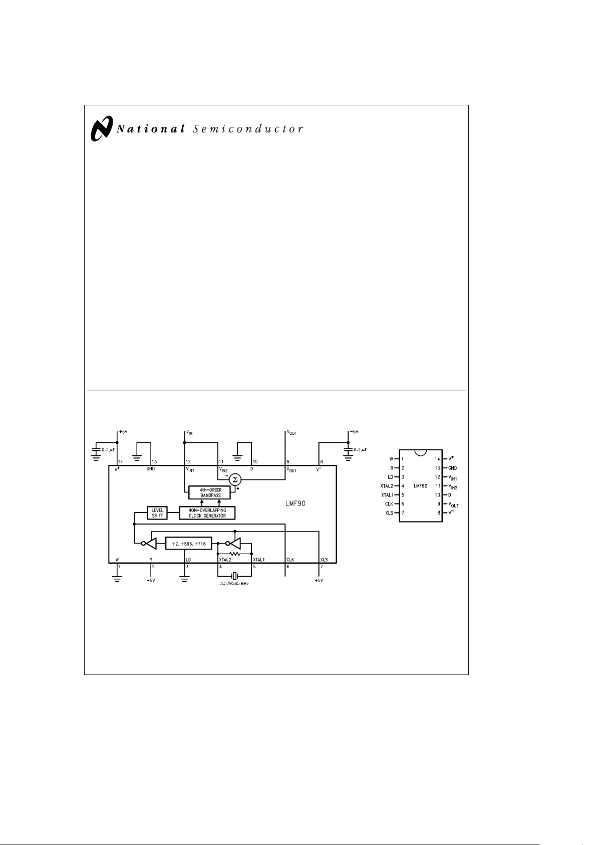
Typical Connection
60 Hz Notch Filter
TL/H/10354– 1
Connection
Diagram
Dual-In-Line and Small
Outline Packages
TL/H/10354– 2
Top View
Order Number LMF90CCN,
LMF90CIWM,
LMF90CCWM, LMF90CIJ,
LMF90CCJ, LMF90CIN,
LMF90CMJ or
LMF90CMJ/883
See NS Package Number
J14A, M14B or N14A
C
1995 National Semiconductor Corporation RRD-B30M115/Printed in U. S. A.
Page 2
Absolute Maximum Ratings (Notes1&3)
If Military/Aerospace specified devices are required, Soldering Information (Note 4)
please contact the National Semiconductor Sales N Package (Soldering, 10 sec.) 260
§
C
Office/Distributors for availability and specifications. J Package (Soldering, 10 sec.) 300
§
C
Supply Voltage (V
S
e
V
a
b
V
b
)
b
0.3V to
a
16V Storage Temperature Range
b
65
§
Cto
a
150
§
C
Voltage at any Input or Output V
b
b
0.3V to V
a
a
0.3V Junction Temperature 150
§
C
Input Current at any Pin (Note 10) 5 mA
Operating Ratings (Notes2&3)
Package Input Current (Note 10) 20 mA
Temperature Range T
MIN
s
T
A
s
T
MAX
Power Dissipation (Note 5) 500 mW
LMF90CCN, LMF90CCWM,
ESD Susceptability (Note 6)
LMF90CCJ 0
§
C
s
T
A
s
a
70
§
C
Pin 9 1800V
LMF90CIJ, LMF90CIWM, LMF90CIN
All Other Pins 2000V
b
40
§
C
s
T
A
s
a
85
§
C
LMF90CMJ, LMF90CMJ/883
b
55
§
C
s
T
A
s
a
125
§
C
Supply Voltage Range 4.0V to 15.0V
AC Electrical Characteristics The following specifications apply for V
a
ea
5V and V
b
eb
5V unless otherwise specified. Boldface limits apply for
T
A
e
T
MIN
to T
MAX
; all other limits T
A
e
T
J
e
25
§
C.
LMF90CCJ, LMF90CCN, LMF90CIJ, LMF90CIWM,
LMF90CCWM LMF90CIN, LMF90CMJ
Units
Symbol Parameter Conditions
Typ
Tested Design
Typ
Tested Design (Limit)
(Note 7)
Limit Limit
(Note 7)
Limit Limit
(Note 8) (Note 9) (Note 8) (Note 9)
f
O
Center Frequency 0.1 0.1 Hz (Min)
Range 30 30 30 kHz (Max)
f
CLK
Clock Frequency Pin 6 10 10 Hz (Min)
Range Pin 6 1.5 1.5 1.5 MHz (Max)
Pins 4 and 5 4.0 4.0 4.0 MHz (Max)
f
CLK
/f
O1
Clock-to-Center- W
e
D
e
V
b
,R
e
V
a
,
33.5
g
1% 33.5
g
1.5% 33.5
g
1.5% (Max)
Frequency Ratio f
CLK
e
167 kHz
f
CLK
/f
O2
W
e
D
e
R
e
GND,
50.25
g
1% 50.25
g
1.5% 50.25
g
1.5% (Max)
f
CLK
e
250 kHz
f
CLK
/f
O3
W
e
V
a
,D
e
GND, R
e
V
b
,
100.5
g
1% 100.5
g
1.5% 100.5
g
1.5% (Max)
f
CLK
e
500 kHz
H
ON
Passband Gain DC and 20 kHz, W
e
D
e
V
b
,R
e
V
a
,
0
g
0.2
g
0.2 0
g
0.2 dB (Max)
f
CLK
e
167 kHz
W
e
D
e
R
e
GND,
0
g
0.2
g
0.2 0
g
0.2 dB (Max)
f
CLK
e
250 kHz
W
e
V
a
,D
e
GND, R
e
V
b
,
0
g
0.2
g
0.2 0
g
0.2 dB (Max)
f
CLK
e
500 kHz
2
Page 3
AC Electrical Characteristics The following specifications apply for V
a
ea
5V and V
b
eb
5V unless otherwise specified. Boldface limits apply for
T
A
e
T
MIN
to T
MAX
; all other limits T
A
e
T
J
e
25
§
C. (Continued)
LMF90CCJ, LMF90CCN, LMF90CIJ, LMF90CIWM,
LMF90CCWM LMF90CIN, LMF90CMJ
Units
Symbol Parameter Conditions
Typ
Tested Design
Typ
Tested Design (Limit)
(Note 7)
Limit Limit
(Note 7)
Limit Limit
(Note 8) (Note 9) (Note 8) (Note 9)
PBW Ratio of Passband W
e
D
e
V
b
,R
e
V
a
,
0.1275
g
0.0175 0.1275
g
0.0175 0.1275
g
0.0175 (Max)
Width to Center f
CLK
e
167 kHz
Frequency W
e
D
e
R
e
GND,
0.265
g
0.025 0.265
g
0.025 0.265
g
0.025 (Max)
f
CLK
e
250 kHz
W
e
V
a
,D
e
GND, R
e
V
b
,
0.550
g
0.05 0.550
g
0.05 0.550
g
0.05 (Max)
f
CLK
e
500 kHz
A
Min1
@
f
O1
Gain at W
e
D
e
V
b
,R
e
V
a
,
b
39
b
30
b
30
b
39
b
30 dB (Max)
Center Frequency f
CLK
e
167 kHz
A
Min2
@
f
O2
W
e
D
e
R
e
GND,
b
48
b
36.5
b
36.5
b
48
b
36.5 dB (Max)
f
CLK
e
250 kHz
A
Min3
@
f
O3
W
e
V
a
,D
e
GND, R
e
V
b
,
b
48
b
36.5
b
36.5
b
48
b
36.5 dB (Max)
f
CLK
e
500 kHz
Additional Center W
e
GND, D
e
V
b
,R
e
V
a
,
b
36
b
30
b
30
b
36
b
30 dB (Max)
Frequency Gain f
CLK
e
167 kHz
Tests at f
O1
W
e
V
a
,D
e
V
b
,R
e
V
a
,
b
36
b
30
b
30
b
36
b
30 dB (Max)
f
CLK
e
167 kHz
W
e
V
b
,D
e
GND, R
e
V
a
,
b
42
b
30
b
30
b
42
b
30 dB (Max)
f
CLK
e
167 kHz
W
e
D
e
GND, R
e
V
a
,
b
48
b
35
b
35
b
48
b
35 dB (Max)
f
CLK
e
167 kHz
W
e
V
a
,D
e
GND,R
e
V
a
,
b
48
b
35
b
35
b
48
b
35 dB (Max)
f
CLK
e
167 kHz
3
Page 4
AC Electrical Characteristics The following specifications apply for V
a
ea
5V and V
b
eb
5V unless otherwise specified. Boldface limits apply for
T
A
e
T
MIN
to T
MAX
; all other limits T
A
e
T
J
e
25
§
C. (Continued)
LMF90CCJ, LMF90CCN, LMF90CIJ, LMF90CIWM,
LMF90CCWM LMF90CIN, LMF90CMJ
Units
Symbol Parameter Conditions
Typ
Tested Design
Typ
Tested Design (Limit)
(Note 7)
Limit Limit
(Note 7)
Limit Limit
(Note 8) (Note 9) (Note 8) (Note 9)
Additional Center W
e
V
b
,D
e
V
b
,R
e
GND,
b
36
b
30
b
30
b
36
b
30 dB (Max)
Frequency Gain f
CLK
e
250 kHz
Tests at f
O2
W
e
GND, D
e
V
b
,R
e
GND,
b
36
b
30
b
30
b
36
b
30 dB (Max)
f
CLK
e
250 kHz
W
e
V
a
,D
e
V
b
,R
e
GND,
b
36
b
30
b
30
b
36
b
30 dB (Max)
f
CLK
e
250 kHz
W
e
V
b
,D
e
R
e
GND,
b
42
b
30
b
30
b
42
b
30 dB (Max)
f
CLK
e
250 kHz
W
e
V
a
,D
e
R
e
GND,
b
48
b
35
b
35
b
48
b
35 dB (Max)
f
CLK
e
250 kHz
Additional Center W
e
D
e
R
e
V
b
,
b
36
b
30
b
30
b
36
b
30 dB (Max)
Frequency Gain f
CLK
e
500 kHz
Tests at f
O3
W
e
GND, D
e
V
b
,R
e
V
b
,
b
36
b
30
b
30
b
36
b
30 dB (Max)
f
CLK
e
500 kHz
W
e
V
a
,D
e
V
b
,R
e
V
b
,
b
36
b
30
b
30
b
36
b
30 dB (Max)
f
CLK
e
500 kHz
W
e
V
b
,D
e
GND, R
e
V
b
,
b
42
b
30
b
30
b
42
b
30 dB (Max)
f
CLK
e
500 kHz
W
e
D
e
GND, R
e
V
b
,
b
48
b
35
b
35
b
48
b
35 dB (Max)
f
CLK
e
500 kHz
A
3a
Gain at f
3
e
0.995 f
O1
W
e
D
e
V
b
,R
e
V
a
,
b
41
b
30
b
30
b
41
b
30 dB (Max)
A
4a
Gain at f
4
e
1.005 f
O1
f
CLK
e
167 kHz
b
41
b
30
b
30
b
41
b
30 dB (Max)
A
3b
Gain at f
3
e
0.992 f
O2
W
e
D
e
R
e
GND, f
CLK
e
250 kHz
b
40
b
35
b
35
b
40
b
35 dB (Max)
A
4b
Gain at f
4
e
1.008 f
O2
b
40
b
35
b
35
b
40
b
35 dB (Max)
A
3c
Gain at f
3
e
0.982 f
O3
W
e
V
a
,D
e
GND, R
e
V
b
b
41
b
35
b
35
b
41
b
35 dB (Max)
A
4c
Gain at f
4
e
1.018 f
O3
f
CLK
e
500 kHz
b
41
b
35
b
35
b
41
b
35 dB (Max)
A
max1
Passband Ripple W
e
D
e
V
b
,R
e
V
a
,f
5
e
0.914 f
O1
0.25 0.9 0.9 0.25 0.9 dB (Max)
f
CLK
e
167 kHz 0.25 0 0 0.25 0 dB (Min)
f
6
e
1.094 f
O1
0.25 0.9 0.9 0.25 0.9 dB (Max)
0.25 0 0 0.25 0 dB (Min)
4
Page 5
AC Electrical Characteristics The following specifications apply for V
a
ea
5V and V
b
eb
5V unless otherwise specified. Boldface limits apply for
T
A
e
T
MIN
to T
MAX
; all other limits T
A
e
T
J
e
25
§
C. (Continued)
LMF90CCJ, LMF90CCN, LMF90CIJ, LMF90CIWM,
LMF90CCWM LMF90CIN, LMF90CMJ
Units
Symbol Parameter Conditions
Typ
Tested Design
Typ
Tested Design (Limit)
(Note 7)
Limit Limit
(Note 7)
Limit Limit
(Note 8) (Note 9) (Note 8) (Note 9)
A
Max2
Passband Ripple W
e
D
e
R
e
GND, f
5
e
0.830 f
O2
0.25 0.9 0.9 0.26 0.9 dB (Max)
f
CLK
e
250 kHz 0.25 0 0 0.25 0 dB (Min)
f
6
e
1.205 f
O2
0.25 0.9 0.9 0.25 0.9 dB (Max)
0.25 0 0 0.25 0 dB (Min)
A
Max3
Passband Ripple W
e
V
a
,D
e
GND, R
e
V
b
f
5
e
0.700 f
O3
0.25 0.9 0.9 0.25 0.9 dB (Max)
f
CLK
e
500 kHz 0.25 0 0 0.25 0 dB (Min)
f
6
e
1.428 f
O3
0.25 0.9 0.9 0.25 0.9 dB (Max)
0.25 0 0 0.25 0 dB (Min)
E
n
Output Noise 20 kHz Bandwidth
W
e
D
e
V
b
,R
e
V
a
,f
CLK
e
167 kHz 670 670 mVrms
W
e
D
e
R
e
GND, f
CLK
e
250 kHz 370 370 mVrms
W
e
V
a
,D
e
GND, R
e
V
b
,
250 250 mVrms
f
CLK
e
500 kHz
Clock Feedthrough 50 50 mVp–p
GBW Output Buffer
1 1 MHz
Gain Bandwidth
SR Output Buffer
33V/ms
Slew Rate
C
L
Maximum Capacitive
200 200 pF
Load
5
Page 6
DC Electrical Characteristics The following specifications apply for V
a
ea
5V and V
b
eb
5V unless otherwise specified. Boldface Limits Apply for
T
A
e
T
MIN
to T
MAX
; all other limits T
A
e
T
J
e
25
§
C.
LMF90CCJ, LMF90CCN, LMF90CIJ, LMF90CIWM,
LMF90CCWM LMF90CIN, LMF90CMJ
Units
Symbol Parameter Conditions
Typ
Tested Design
Typ
Tested Design (Limit)
(Note 7)
Limit Limit
(Note 7)
Limit Limit
(Note 8) (Note 9) (Note 8) (Note 9)
I
S
Power Supply Current f
CLK
e
500 kHz, V
IN1
e
V
IN2
e
GND 2.35 5.0 5.0 2.35 5.0 mA (Max)
V
OS
Output Offset Voltage W
e
D
e
V
b
,R
e
V
a
,f
CLK
e
167 kHz
g
50
g
120
g
120
g
50
g
120 mV (Max)
W
e
D
e
R
e
GND, f
CLK
e
250 kHz
g
60
g
140
g
140
g
60
g
140 mV (Max)
W
e
V
a
,D
e
GND, R
e
V
b
,
g
80
g
170
g
170
g
80
g
170 mV (Max)
f
CLK
e
500 kHz
V
OUT
Output Voltage Swing R
L
e
5kX
a
4.2,
b
4.7
g
4.0
g
4.0
a
4.2,
b
4.7
g
4.0 V (Min)
V
I1
Logical ‘‘Low’’ Pins 1, 2, 3, 7, and 10
b
4.0
b
4.0
b
4.0 V (Max)
Input Voltage
V
I2
Logical ‘‘GND’’ Pins 1, 2, 3, 7, and 10
a
1.0
a
1.0
a
1.0 V (Max)
Input Voltage
b
1.0
b
1.0
b
1.0 V (Min)
V
I3
Logical ‘‘High’’ Pins 1, 2, 3, and 7
a
4.0
a
4.0
a
4.0 V (Min)
Input Voltage
I
IN
Input Current Pins 1, 2, 3, 7, and 10
g
10
g
10
g
10 mA (Max)
V
IL
Logical ‘‘0’’ Input Pin 5, XLS
e
V
a
b
4.0
b
4.0
b
4.0 V (Max)
Voltage, Pins 5 and 6 or Pin 6, XLS
e
GND
V
IH
Logical ‘‘1’’ Input
a
4.0
a
4.0
a
4.0 V(Min)
Voltage, Pins 5 and 6
V
IL
Logical ‘‘0’’ Input V
a
b
V
b
e
10V, XLS
e
V
b
or
a
0.8
a
0.8
a
0.8 V (Max)
Voltage, Pin 6 V
a
ea
5V, V
b
e
0V, XLS
ea
2.5V
V
IH
Logical ‘‘1’’ Input
a
2.0
a
2.0
a
2.0 V (Min)
Voltage, Pin 6
V
OL
Logical ‘‘0’’ Output XLS
e
V
a
,
l
I
OUT
l
e
4mA
b
4.0
b
4.0
b
4.0 V (Max)
Voltage, Pin 6
V
OH
Logical ‘‘1’’ Output
a
4.0
a
4.0
a
4.0 V (Min)
Voltage, Pin 6
6
Page 7

DC Electrical Characteristics (Continued)
Note 1: Absolute Maximum Ratings indicate limits beyond which damage to the device may occur.
Note 2: Operating Ratings indicate conditions for which the device is intended to be functional. These ratings do not guarantee specific performance limits,
however. For guaranteed specifications and test conditions, see the Electrical Characteristics. The guaranteed specifications apply only for the test conditions
listed. Some performance characteristics may degrade when the device is not operated under the listed test conditions.
Note 3: All voltages are measured with respect to GND unless otherwise specified.
Note 4: See AN450 ‘‘Surface Mounting Methods and Their Effect on Product Reliability’’ or the section titled ‘‘Surface Mount’’ found in any current Linear Data
Book for other methods of soldering surface mount devices.
Note 5: The maximum power dissipation must be derated at elevated temperatures and is dictated by T
JMAX
, HJAand the ambient temperature, TA. The maximum
allowable power dissipation at any temperature is P
D
e
(T
JMAX
b
TA)/HJAor the number given in the Absolute Maximum Ratings, whichever is lower. For this
device, T
JMAX
e
150§C, and the typical thermal resistance (HJA) when board mounted is 61§C/W for the LMF90CCN and CIN, 134§C/W for the LMF90CCWM and
CWIM and 59
§
C/W for the LMF90CCJ, CIJ and CMJ.
Note 6: Human body model, 100 pF discharged through a 1.5 kX resistor.
Note 7: Typicals are at T
J
e
25§C and represent the most likely parametric norm.
Note 8: Tested Limits are guaranteed and 100% tested.
Note 9: Design Limits are guaranteed, but not 100% tested.
Note 10: When the input voltage (V
IN
) at any pin exceeds the power supplies (V
IN
k
Vbor V
IN
l
Va), the current at that pin should be limited to 5 mA. The 20 mA
maximum package input current rating limits the number of pins that can safely exceed the power supplies with an input current of 5 mA to four.
7
Page 8

Typical Performance Characteristics
Clock Frequency
Notch Depth vs
Supply Voltage
Notch Depth vs
vs Temperature
Notch Depth
vs Power Supply Voltage
Power Supply Current
vs Temperature
Power Supply Current
Clock Frequency
Offset Voltage vs
Supply Voltage
Offset Voltage vs
Temperature
Offset Voltage vs
Clock Frequency
Passband Width vs
Supply Voltage
Passband Width vs
Temperature
Passband Width vs
Clock Frequency
Stopband Width vs
TL/H/10354– 3
8
Page 9

Typical Performance Characteristics (Continued)
vs Supply Voltage
Stopband Width
vs Temperature
Stopband Width
vs Clock Frequency
Ratio Deviation
Clock-to-Center-Frequency
vs Supply Voltage
Ratio Deviation
Clock-to-Center-Frequency
vs Temperature
Ratio Deviation
Clock-to-Center-Frequency
vs Supply Voltage
Output Swing
Swing vs Load Resistance
Positive Output Voltage
Swing vs Load Resistance
Negative Output Voltage
vs Temperature
Positive Output Swing
vs Temperature
Negative Output Swing
TL/H/10354– 4
9
Page 10

Pin Descriptions
W (Pin 1) This three-level logic input sets the width of
the notch. Notch width is f
c2–fc1
(see
Figure
1
). When W is tied to Va(pin 14), GND (pin
13), or V
b
(pin 8), the notch width is 0.55 f0,
0.26 f
0
, or 0.127 f0, respectively.
R (Pin 2) This three-level logic input sets the ratio of
the clock frequency (f
CLK
) to the center fre-
quency (f
0
). When R is tied to Va, GND, or
V
b
, the clock-to-center-frequency ratio is
33.33:1, 50:1, or 100:1, respectively.
LD (Pin 3) This three-level logic input sets the division
factor of the clock frequency divider. When
LD is tied to V
a
, GND, or Vb, the division
factor is 716, 596, or 2, respectively.
XTAL2 (Pin 4) This is the output of the internal crystal os-
cillator. When using the internal oscillator,
the crystal should be tied between XTAL2
and XTAL1. (The capacitors are internalÐ
no external capacitors are needed for the
oscillator to operate.) When not using the
internal oscillator this pin should be left
open.
XTAL1 (Pin 5) This is the crystal oscillator input. When us-
ing the internal oscillator, the crystal should
be tied between XTAL1 and XTAL2. XTAL1
can also be used as an input for an external
clock signal swinging from V
a
to Vb. The
frequency of the crystal or the external
clock will be divided internally by the clock
divider as determined by the programming
voltage on pin 3.
CLK (Pin 6) This is the filter clock pin. The clock signal
appearing on this pin is the filter clock
(f
CLK
). When using the internal crystal oscillator or an external clock signal applied to
pin 5 while pin 7 is tied to V
a
, the CLK pin is
the output of the divider and can be used to
drive other LMF90s with its rail-to-rail output
swing. When not using the internal crystal
oscillator or an external clock on pin 5, the
CLK pin can be used as a CMOS or TTL
clock input provided that pin 7 is tied to
GND or V
b
. For best performance, the duty
cycle of a clock signal applied to this pin
should be near 50%, especially at higher
clock frequencies.
XLS (Pin 7) This is a three-level logic pin. When XLS is
tied to V
a
, the crystal oscillator and frequency divider are enabled and CLK (pin 6)
is an output. When XLS is tied to GND (pin
13), the crystal oscillator and frequency divider are disabled and pin 6 is an input for a
clock swinging between V
b
and Va. When
XLS is tied to V
b
, the crystal oscillator and
frequency divider are disabled and pin 6 is a
TTL level clock input for a clock signal
swinging between GND and V
a
or between
V
b
and GND.
V
b
(Pin 8) This is the negative power supply pin. It
should be bypassed with at least a 0.1 mF
capacitor. For single-supply operation,
connect this pin to system ground.
V
OUT
(Pin 9) This is the filter output.
D (Pin 10) This two-level logic input is used to set the
depth of the notch (the attenuation at f
0
).
When D is tied to GND or V
b
, the typical
notch depth is 48 dB or 39 dB, respectively. Note, however, that the notch depth is
also dependent on the width setting (pin
1). See the Electrical Characteristics for
tested limits.
V
IN2
(Pin 11) This is the input to the difference amplifier
section of the notch filter.
V
IN1
(Pin 12) This is the input to the internal bandpass
filter. This pin is normally connected to pin
11. For wide bandwidth applications, an
anti-aliasing filter can be inserted between
pin 11 and pin 12.
GND (Pin 13) This is the analog ground reference for the
LMF90. In split supply applications, GND
should be connected to the system
ground. When operating the LMF90 from a
single positive power supply voltage, pin
13 should be connected to a ‘‘clean’’ reference voltage midway between V
a
and
V
b
.
Va(Pin 14) This is the positive power supply pin. It
should be bypassed with at least a 0.1 mF
capacitor.
1.0 Definition of Terms
A
max
: the maximum amount of gain variation within the fil-
ter’s passband (See
Figure 1
). For the LMF90, A
Max
is
nominally equal to 0.25 dB.
A
min
: the minimum attenuation within the notch’s stopband.
(See
Figure 1
). This parameter is adjusted by programming
voltage applied to pin 10 (D).
Bandwidth (BW) or Passband Width: the difference in frequency between the notch filter’s two cutoff frequencies.
Cutoff Frequency: for a notch filter, one of the two frequencies, f
C1
and fC2that define the edges of the passband. At these two frequencies, the filter has a gain equal to
the passband gain.
f
CLK
: the frequency of the clock signal that appears at the
CLK pin. This frequency determines the filter’s center frequency. Depending on the programming voltage on pin 2
(R), f
CLK
will be either 33.33, 50, or 100 times the center
frequency of the notch.
f
0
or f
Notch
: the center frequency of the notch filter. This
frequency is measured by finding the two frequencies for
which the gain
b
3 dB relative to the passband gain, and
calculating their geometrical mean.
Passband: for a notch filter, frequencies above the upper
cutoff frequency (f
C2
in
Figure 1
) and below the lower cutoff
frequency (f
C1
in
Figure 1
).
10
Page 11

1.0 Definition of Terms (Continued)
Passband Gain: the notch filter’s gain for signal frequen-
cies near dc or f
CLK
/2. The passband gain of a notch filter is
also called ‘‘H
ON
’’. For the LMF90, the passband gain is
nominally 0 dB.
Passband Ripple: the variation in gain within the filter’s
passband.
Stopband: for a notch filter, the range of frequencies for
which the attenuation is at least A
min(fS1
to fS2)in
Figure
1
).
Stop Frequency: one of the two frequencies (f
S1
and fS2)
at the edges of the notch’s stopband.
Stopband Width (SBW): the difference in frequency between the two stopband edges (f
S2–fS1
).
TL/H/10354– 5
FIGURE 1. General Form of Notch Response
2.0 Applications Information
2.1 FUNCTIONAL DESCRIPTION
The LMF90 uses switched-capacitor techniques to realize a
fourth-order elliptic notch transfer function with 0.25 dB
passband ripple. No external components other than supply
bypass capacitors and a clock (or crystal) are required.
As is evident from the block diagram, the analog signal path
consists of a fourth-order bandpass filter and a summing
amplifier. The analog input signal is applied to the input of
the bandpass filter, and to one of the summing amplifier
inputs. The bandpass filter’s output drives the other summing amplifier input. The output of the summing amplifier is
the difference between the input signal and the bandpass
output, and has a notch filter characteristic. Notch width and
depth are controlled by the dc programming voltages applied to two pins (1 and 10), and the center frequency is
proportional to the clock frequency, which may be generated externally or internally with the aid of an external crystal.
The clock-to-center-frequency ratio can be one of three different values, and is selected by the voltage on a three-level
logic input (pin 2).
The clock signal passes through a digital frequency divider
circuit that can divide the clock frequency by any of three
different factors before it reaches the filters. This divider can
also be disabled, if desired. Pin 7 enables and disables the
frequency divider and also configures the clock inputs for
operation with an external CMOS or TTL clock or with the
internal oscillator circuit.
TL/H/10354– 6
FIGURE 2. LMF90 Block Diagram
11
Page 12

2.0 Applications Information (Continued)
2.2 PROGRAMMING PINS
The LMF90 has five control pins that are used to program
the filter’s characteristics via a three-level logic scheme. In
dual-supply applications, these inputs are tied to either V
a
,
V
b
, or GND in order to select a particular set of characteristics. For example, the W input (pin 1) sets the filter’s passband width to 0.55 f
0
, 0.26 f0or 0.127 f0when the W input is
connected to V
a
, GND, or Vb, respectively. Applying V
b
and GND to the D input (pin 10) will set the notch depth to
40 dB or 30 dB, respectively.
The R input (pin 2) is another three-level logic input, and it
sets the clock-to-center-frequency ratio to 33.33:1, 50:1, or
100:1 for input voltages equal to V
a
, GND, or Vb, respectively. Note that the clock frequency referred to here is the
frequency at the CLK pin and at the frequency divider output
(if used). This is different from the frequency at the divider’s
input. LD (pin 3) sets the frequency divider’s division factor
to either 716, 596, or 2 for input voltages equal to V
a
, GND,
or V
b
, respectively. XLS (pin 7) enables and disables the
crystal oscillator and clock divider. When XLS is connected
to the positive supply, the oscillator and divider are enabled,
and CLK is the output of the divider and can drive the clock
inputs of other LMF90s. When XLS is connected to GND,
the oscillator and divider are disabled, and the CLK pin becomes a clock input for CMOS-level signals. Connecting
XLS to the negative supply disables the oscillator and divider and causes CLK to operate as a TTL-level clock input.
Using an external 3.579545 MHz color television crystal with
the internal oscillator and divider, it is possible to build a
power line frequency notch for 50 Hz or 60 Hz line frequencies or their second and third harmonics using the LMF90. A
60 Hz notch is shown in the Typical Application circuit on
the first page of this data sheet. Connecting LD to V
a
changes the notch frequency to 50 Hz. Changing the clockto-center-frequency ratio to 50:1 results in a second-harmonic notch, and a 33:1 ratio causes the LMF90 to notch
the third harmonic.
Table I illustrates 18 different combinations of filter bandwidth, depth, and clock-to-center-frequency ratio obtained
by choosing the appropriate W, D, and R programming voltages.
2.3 DIGITAL INPUTS AND OUTPUTS
As mentioned above, the CLK pin can serve as either an
input or an output, depending on the programming voltage
on XLS. When CLK is operating as a TTL input, it will operate properly in both dual-supply and single-supply applications, because it has two logic thresholdsÐone referred to
V
b
, and one referred to GND. When operating as an output,
CLK swings rail-to-rail (CMOS logic levels).
XTAL1 and XTAL2 are the input and output pins for the
internal crystal oscillator. When using the internal oscillator
(XLS connected to V
a
), the crystal is connected between
these two pins. When the internal oscillator is not used,
XTAL2 should be left open. XTAL1 can be used as an input
for an external CMOS-level clock signal swinging from V
b
to Va. The frequency of the crystal or the external clock
applied to XTAL1 will be divided by the internal frequency
divider as determined by programming voltage on the LD
pin.
2.4 SAMPLED-DATA SYSTEM CONSIDERATIONS
OUTPUT STEPS
Because the LMF90 uses switched-capacitor techniques, its
performance differs in several ways from non-sampled (continuous) circuits. The analog signal at the input to the internal bandpass filter (pin 12) is sampled during each clock
cycle, and, since the output voltage can change only once
every clock cycle, the result is a discontinuous output signal.
The bandpass output takes the form of a series of voltage
‘‘steps’’, as shown in
Figure 3
. The steps are smaller when
the clock frequency is much greater than the signal frequency.
Switched-capacitor techniques are used to set the summing
amplifier’s gain. Its input and feedback ‘‘resistors’’ are actually made from switches and capacitors. Two sets of these
‘‘resistors’’ are alternated during each clock cycle. Each
time these gain-setting components are switched, there will
be no feedback connected to the op amp for a short period
of time (about 50 ns). This generates very low-amplitude
output signals at f
CLK
a
fIN,f
CLK
b
fIN,2f
CLK
a
fIN, etc.
The amplitude of each of these intermodulation components will typically be at least 70 dB below the input signal
amplitude and well beyond the spectrum of interest.
TABLE I. Operation of LMF90 Programming Pins. Values given are for nominal levels of attenuation.
RV
b
(f
CLK/f0
e
100) GND (f
CLK/f0
e
50) Va(f
CLK/f0
e
33.33)
DW
A
min
BW/f
0
SBW/f
0
A
min
BW/f
0
SBW/f
0
A
min
BW/f
0
SBW/f
0
(dB) (dB) (dB)
V
b
b
30 0.12 0.019
b
30 0.12 0.019
b
30 0.12 0.019
V
b
GND
b
30 0.26 0.040
b
30 0.26 0.040
b
30 0.26 0.040
V
a
b
30 0.55 0.082
b
30 0.55 0.082
b
30 0.55 0.082
V
b
b
35 0.12 0.010
b
35 0.12 0.010
b
35 0.12 0.010
GND GND
b
40 0.26 0.024
b
40 0.26 0.024
b
40 0.26 0.024
V
a
b
40 0.55 0.050
b
40 0.55 0.050
b
40 0.55 0.050
12
Page 13

2.0 Applications Information (Continued)
ALIASING
Another important characteristic of sampled-data systems is
their effect on signals at frequencies greater than one-half
the sampling frequency. (The LMF90’s sampling frequency
is the same as the filter’s clock frequency. This is the frequency at the CLK pin). If a signal with a frequency greater
than one-half the sampling frequency is applied to the input
of a sampled-data system, it will be ‘‘reflected’’ to a frequency less than one-half the sampling frequency. Thus, an input
signal whose frequency is f
S
/2a10 Hz will cause the sys-
tem to respond as though the input frequency was f
s
/2
b
10 Hz. This phenomenon is known as ‘‘aliasing’’. Aliasing
can be reduced or eliminated by limiting the input signal
spectrum to less than f
s
/2.
In some cases, it may be necessary to use a bandwidth
limiting filter (often a simple passive RC low-pass) ahead of
the bandpass input. Although the summing amplifier uses
switched-capacitor techniques, it does not exhibit aliasing
behavior, and the anti-aliasing filter need not be in its input
signal path. The filter can be placed ahead of pin 12 as
shown in
Figure 4
, with the non-band limited input signal
applied to pin 11. The output spectrum will therefore be
wideband, although limited by the bandwidth of the summing amplifier’s output buffer amplifier (typically 1 MHz),
even if f
CLK
is less than 1 MHz. Phase shift in the anti-alias-
ing filter will affect the accuracy of the notch transfer func-
tion, however, so it is best to use the highest available
clock-to-center-frequency ratio (100:1) and set the RC filter
cutoff frequency to about 15 to 20 times the notch frequency. This will provide reasonable attenuation of high-frequency input signals, while avoiding degradation of the overall
notch response. If the anti-aliasing filter’s cutoff frequency is
too low, it will introduce phase shift and gain errors large
enough to shift the frequency of the notch and reduce its
depth. A cutoff frequency that is too high may not provide
sufficient attenuation of unwanted high-frequency signals.
TL/H/10354– 7
FIGURE 3. Output waveform of a switched-capacitor
filter. Note the voltage steps caused by sampling
at the clock frequency.
TL/H/10354– 8
FIGURE 4. Using a simple passive low-pass filter to prevent aliasing in the presence of high-frequency input signals.
13
Page 14

2.0 Applications Information (Continued)
NOISE
Switched-capacitor filters have two kinds of noise at their
outputs. There is a random, ‘‘thermal’’ noise component
whose level is typically on the order of hundreds of microvolts. The other kind of noise is digital clock feedthrough.
This will have an amplitude in the vicinity of 50 mV peak-topeak. In some applications, the clock noise frequency is so
high compared to the signal frequency that it is unimportant.
In other cases, clock noise may have to be removed from
the output signal with, for example, a passive low-pass filter
at the LMF90’s output pin.
CLOCK FREQUENCY LIMITATIONS
The performance characteristics of a switched-capacitor filter depend on the switching (clock) frequency. At very low
clock frequencies (below 10 Hz), the time between clock
cycles is relatively long, and small parasitic leakage currents
cause the internal capacitors to discharge sufficiently to affect the filter’s offset voltage and gain. This effect becomes
more pronounced at elevated operating temperatures.
At higher clock frequencies, performance deviations are primarily due to the reduced time available for the internal operational amplifiers to settle. Best performance with high
clock frequencies will be obtained when the filter clock’s
duty cycle is 50%. The clock frequency divider, when used,
provides a 50% duty cycle clock to the filter, but when an
external clock is applied to CLK, it should have a duty cycle
close to 50% for best performance.
Input Impedance
The input to the bandpass section of the LMF90 (V
IN1
)is
similar to the switched-capacitor circuit shown in
Figure 5
.
During the first half of a clock cycle, the i
1
switch closes,
charging C
IN
to the input voltage VIN. During the second
half-cycle, the i
2
switch closes, and the charge on CINis
transferred to the feedback capacitor. At frequencies well
below the clock frequency, the input impedance approximates a resistor whose value is
R
IN
e
1
CINf
CLK
.
At the bandpass filter input, C
IN
is nominally 3.0 pF. For a
worst-case calculation of effective R
IN
, assume C
IN
e
3.0 pF and f
CLK
e
1.5 MHz. Thus,
R
IN
(Min)
e
1
4.5x10
b
6
e
222 kX.
At the maximum clock frequency of 1.5 MHz, the lowest
typical value for the effective R
IN
at the V
IN1
input is there-
fore 222 kX. Note that R
IN
increases as f
CLK
decreases, so
the input impedance will be greater than or equal to this
value. Source impedance should be low enough that this
input impedance doesn’t significantly affect gain.
The summing amplifier input impedance at V
IN2
is calculat-
ed in a similar manner, except that C
IN
e
5.0 pF. This yields
a minimum input impedance of 133 kX at V
IN2
. When both
inputs are connected together, the combined input impedance will be 83.3 kX with a 1.5 MHz filter clock.
TL/H/10354– 9
FIGURE 5. Simplified LMF90 bandpass section input
stage. At frequencies well below the center frequency,
the input impedance appears to be resistive.
2.5 POWER SUPPLY AND CLOCK OPTIONS
The LMF90 is designed to operate from either single or dual
power supply voltages from 5V to 15V. In either case, the
supply pins should be well-bypassed to minimize any feedthrough of power supply noise into the filter’s signal path.
Such feedthrough can significantly reduce the depth of the
notch. For operation from dual supply voltages, connect V
b
(pin 8) to the negative supply, GND (pin 13) to the system
ground, and V
a
to the positive supply.
For single supply operation, simply connect Vbto system
ground and GND (Pin 13) to a ‘‘clean’’ reference voltage at
mid-supply. This reference voltage can be developed with a
pair of resistors and a capacitor as shown in
Figures 10
through16. Note that for single supply operation, the threelevel logic inputs should be connected to system ground
and V
a
/2 instead of Vband GND. The CLK input will operate properly with TTL-level clock signals when the LMF90 is
powered from either single or dual supplies because it has
two TTL thresholds, one referred to the V
b
pin and one
referred to the GND pin. XLS should be connected to the
V
b
pin when an external TTL clock is used.
Figures 6
through16illustrate a wide variety of power supply and
clock options.
14
Page 15

2.0 Applications Information (Continued)
DUAL-SUPPLY CLOCK OPTIONS
TL/H/10354– 10
FIGURE 6. Dual supply; external CMOS-level clock. Internal frequency divider disabled.
TL/H/10354– 11
FIGURE 7. Dual supply; TTL-level clock. Internal frequency divider disabled.
15
Page 16

2.0 Applications Information (Continued)
DUAL-SUPPLY CLOCK OPTIONS
TL/H/10354– 12
FIGURE 8. Dual Supply; external CMOS-level clock. Internal frequency divider enabled.
Output of logic divider available on pin 6.
TL/H/10354– 13
FIGURE 9. Dual supply; internal crystal clock oscillator.
Internal frequency divider enabled. Output of logic divider available on pin 6.
16
Page 17

2.0 Applications Information (Continued)
SINGLE-SUPPLY CLOCK OPTIONS
TL/H/10354– 14
FIGURE 10. Singlea5V supply; external TTL-level clock. Internal frequency divider disabled.
FIGURE 11. Singlea5V supply; external CMOS-level clock. TL/H/10354– 15
Internal frequency divider enabled. Output of logic divider available on pin 6.
17
Page 18

2.0 Applications Information (Continued)
SINGLE-SUPPLY CLOCK OPTIONS
TL/H/10354– 16
FIGURE 12. Singlea10V supply; external TTL-level clock. Internal frequency divider disabled.
TL/H/10354– 17
FIGURE 13. Singlea10V supply; external CMOS-level clock. Internal frequency divider disabled.
18
Page 19

2.0 Applications Information (Continued)
SINGLE-SUPPLY CLOCK OPTIONS
TL/H/10354– 18
FIGURE 14. Singlea10V supply; external CMOS-level clock.
Internal frequency divider enabled. Output of logic divider available on pin 6.
TL/H/10354– 19
FIGURE 15. Singlea5V ora10V supply; internal crystal clock oscillator. Internal frequency divider enabled.
Output of logic divider available on pin 6.
19
Page 20

Typical Application
TL/H/10354– 20
FIGURE 16. 50 Hz and 150 Hz Notch Filter
20
Page 21

Physical Dimensions inches (millimeters)
14 Lead Ceramic Dual-In-Line Package (J)
Order Number LMF90CIJ, LMF90CMJ, LMF90CMJ/883 or LMF90CCJ
NS Package Number J14A
14 Lead Molded Package, Small Outline, 0.300×Wide
Order Number LMF90CCWM or LMF90CIWM
NS Package Number M14B
21
Page 22

LMF90 4th-Order Elliptic Notch Filter
Physical Dimensions inches (millimeters) (Continued)
14 Lead Molded Dual-In-Line Package (N)
Order Number LMF90CCN or LMF90CIN
NS Package Number N14A
LIFE SUPPORT POLICY
NATIONAL’S PRODUCTS ARE NOT AUTHORIZED FOR USE AS CRITICAL COMPONENTS IN LIFE SUPPORT
DEVICES OR SYSTEMS WITHOUT THE EXPRESS WRITTEN APPROVAL OF THE PRESIDENT OF NATIONAL
SEMICONDUCTOR CORPORATION. As used herein:
1. Life support devices or systems are devices or 2. A critical component is any component of a life
systems which, (a) are intended for surgical implant support device or system whose failure to perform can
into the body, or (b) support or sustain life, and whose be reasonably expected to cause the failure of the life
failure to perform, when properly used in accordance support device or system, or to affect its safety or
with instructions for use provided in the labeling, can effectiveness.
be reasonably expected to result in a significant injury
to the user.
National Semiconductor National Semiconductor National Semiconductor National Semiconductor
Corporation Europe Hong Kong Ltd. Japan Ltd.
1111 West Bardin Road Fax: (
a
49) 0-180-530 85 86 13th Floor, Straight Block, Tel: 81-043-299-2309
Arlington, TX 76017 Email: cnjwge@tevm2.nsc.com Ocean Centre, 5 Canton Rd. Fax: 81-043-299-2408
Tel: 1(800) 272-9959 Deutsch Tel: (
a
49) 0-180-530 85 85 Tsimshatsui, Kowloon
Fax: 1(800) 737-7018 English Tel: (
a
49) 0-180-532 78 32 Hong Kong
Fran3ais Tel: (
a
49) 0-180-532 93 58 Tel: (852) 2737-1600
Italiano Tel: (
a
49) 0-180-534 16 80 Fax: (852) 2736-9960
National does not assume any responsibility for use of any circuitry described, no circuit patent licenses are implied and National reserves the right at any time without notice to change said circuitry and specifications.
 Loading...