

Page 1
TL/H/11123
LMF380 Triple One-Third Octave Switched-Capacitor Active Filter
November 1995
LMF380 Triple One-Third Octave
Switched-Capacitor Active Filter
General Description
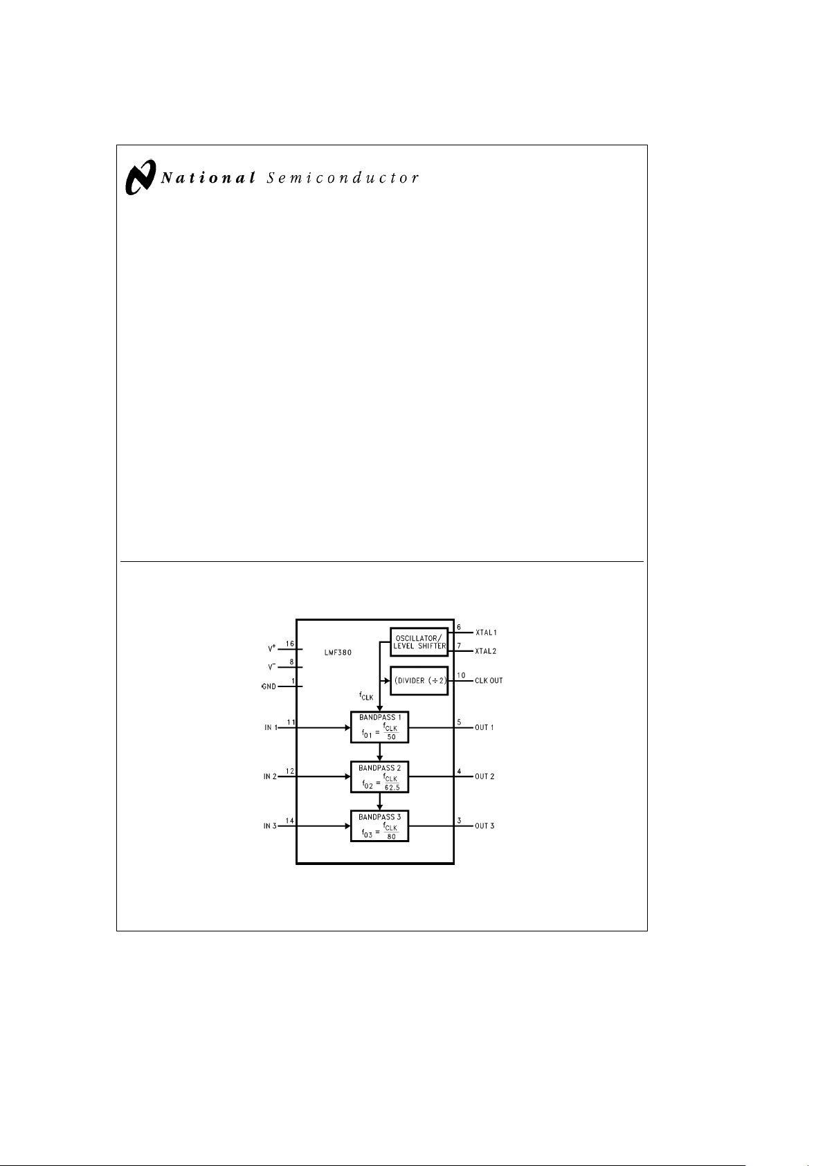
The LMF380 is a triple, one-third octave filter set designed
for use in audio, audiological, and acoustical test and measurement applications. Built using advanced switched-capacitor techniques, the LMF380 contains three filters, each
having a bandwidth equal to one-third of an octave in frequency. By combining several LMF380s, each covering a
frequency range of one octave, a filter set can be implemented that encompasses the entire audio frequency range
while using only a small fraction of the number of components and circuit board area that would be required if a conventional active filter approach were used. The center frequency range is not limited to the audio band, however.
Center frequencies as low as 0.125 Hz or as high as 25 kHz
are attainable with the LMF380.
The center frequency of each filter is determined by the
clock frequency. The clock signal can be supplied by an
external source, or it can be generated by the internal oscillator, using an external crystal and two capacitors. Since the
LMF380 has an internal clock frequency divider (
d
2) and
an output pin for the half-frequency clock signal, a single
clock oscillator for the top-octave LMF380 becomes the
master clock for the entire array of filters in a multiple
LMF380 application.
Accuracy is enhanced by close matching of the internal
components: the ratio of the clock frequency to the center
frequency is typically accurate to
g
0.5%, and passband
gain and stopband attenuation are guaranteed over the full
temperature range.
Features
Y
Three bandpass filters with one-third octave center frequency spacing
Y
Choice of internal or external clock
Y
No external components other than clock or crystal and
two capacitors
Key Specifications
Y
Passband gain accuracy: Better than 0.7 dB over
temperature
Y
Supply voltage range:g2V tog7.5V ora4V toa14V
Applications
Y
Real-Time Audio Analyzers (ANSI Type E, Class II)
Y
Acoustical Instrumentation
Y
Noise Testing
Simplified Block Diagram
TL/H/11123– 1
C
1995 National Semiconductor Corporation RRD-B30M115/Printed in U. S. A.
Page 2
Absolute Maximum Ratings (Notes1&2)
If Military/Aerospace specified devices are required,
please contact the National Semiconductor Sales
Office/Distributors for availability and specifications.
Total Supply Voltage
b
0.3V toa16V
Voltage at Any Pin V
b
b
0.3V to V
a
a
0.3V
Input Current per Pin (Note 3)
g
5mA
Total Input Current (Note 3)
g
20 mA
Lead Temperature (Soldering 10 sec.)
Dual-In-Line Package (Plastic) 300§C
Surface Mount Package (Note 4)
Vapor Phase (60 seconds) 215
§
C
Infrared (15 seconds) 220
§
C
Power Dissipation (Note 5) 500 mW
Maximum Junction Temperature 150
§
C
Storage Temperature Range
b
65§Ctoa150§C
ESD Susceptibility (Note 6) 2000V
Operating Ratings (Note 1)
Temperature Range T
MIN
s
T
A
s
T
MAX
LMF380CIN, LMF380CIV,
LMF380CIJ
b
40§CsT
A
s
a
85§C
LMF380CMJ
b
55§CsT
A
s
a
125§C
Supply Voltage (V
a
b
Vb) 4.0V to 14V
Clock Input Frequency 10 Hz to 1.25 MHz
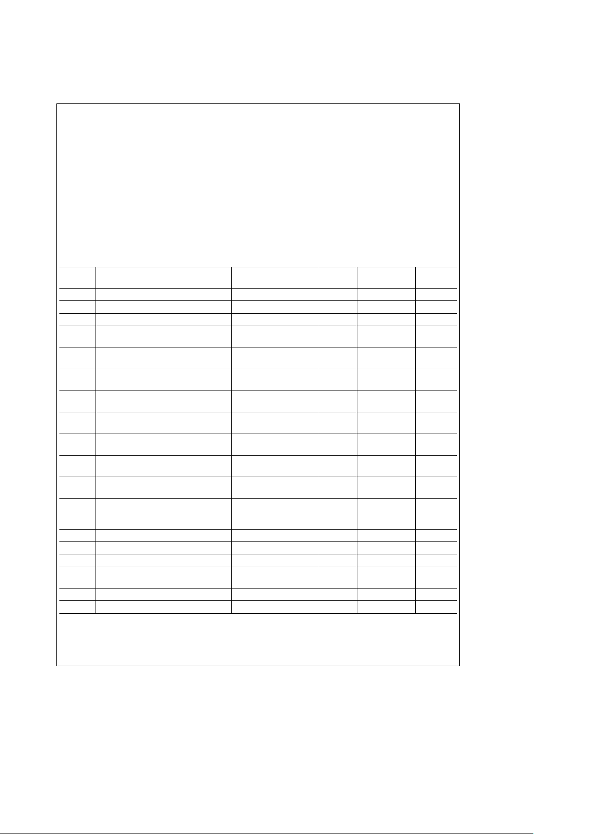
Filter Electrical Characteristics The following specifications apply for V
a
ea
5V, V
b
eb
5V, and f
CLK
e
320 kHz unless otherwise specified. Boldface limits apply for T
MIN
to T
MAX
; all other limits apply for T
A
e
T
J
e
25§C.
Symbol Parameter Conditions
Typical Limit Units
(Note 7) (Note 8) (Limit)
f
CLK:f01
Clock-to-Center-Frequency Ratio, Filter 1 50:1
f
CLK:f02
Clock-to-Center-Frequency Ratio, Filter 2 62.5:1
f
CLK:f03
Clock-to-Center-Frequency Ratio, Filter 3 80:1
A
1
Gain at f
1
e
3720 Hz (Filter 1), (Note 9)
b
32
b
30 dB (max)
2960 Hz (Filter 2), 2340 Hz (Filter 3)
A
2
Gain at f
2
e
6080 Hz (Filter 1), (Note 9)
a
0.1 0.1g0.7 dB (max)
4820 Hz (Filter 2), 3820 Hz (Filter 3)
A
3
Gain at f
3
e
6200 Hz (Filter 1), (Note 9
0.0
b
0.0g0.7 dB (max)
4960 Hz (Filter 2), 3940 Hz (Filter 3)
A
4
Gain at f
4
e
6400 Hz (Filter 1), (Note 9)
b
0.2
b
0.2
g
0.7 dB (max)
5080 Hz (Filter 2), 4040 Hz (Filter 3)
A
5
Gain at f
5
e
6540 Hz (Filter 1), (Note 9)
b
0.1
b
0.1g0.7 dB (max)
5180 Hz (Filter 2), 4120 Hz (Filter 3)
A
6
Gain at f
6
e
6720 Hz (Filter 1), (Note 9)
a
0.15
b
0.15g0.7 dB (max)
5340 Hz (Filter 2), 4240 Hz (Filter 3)
A
7
Gain at f
7
e
8900 Hz (Filter 1), (Note 9)
b
22
b
20 dB (max)
7060 Hz (Filter 2), 5600 Hz (Filter 3)
V
OS
Output Offset Voltage, Each Filter
a
50
a
120 mV (max)
b
30 mV (min)
En Total Output Noise, OUT1 0.1 Hz to 20 kHz 240
Total Output Noise, OUT2 210 mVrms
Total Output Noise, OUT3 190
C
L
Maximum Capacitive Load 200 pF
Crosstalk V
IN
e
1 Vrms, fef
O
b
67 dB
Clock Feedthrough, Each Filter V
a
ea
5V, V
b
eb
5V 10 mV
p-p
V
OUT
Output Voltage Swing R
L
e
5kX
a
4.2
a
3.8 V (min)
b
4.6
b
4.2 V (max)
THD Total Harmonic Distortion V
IN
e
1 Vrms, fef
O
0.05 %
I
S
Supply Current 6.0 9.0 mA (max)
2
Page 3
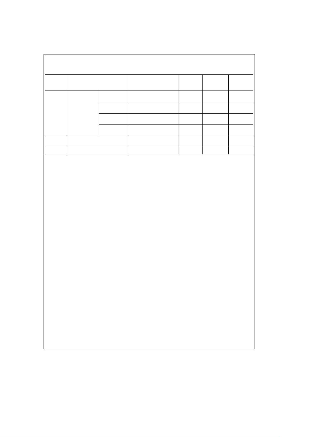
Logic Input and Output Electrical Characteristics
The following specifications for V
a
ea
5V and V
b
eb
5V unless otherwise specified. Boldface limits apply for T
MIN
to
T
MAX
; all other limits apply for T
A
e
T
J
ea
25§C.
Symbol Parameter Conditions
(Note 7)
Typical
Tested
(Limit)
Units
Limit
(Note 8)
V
IH
XTAL1 Logical ‘‘1’’ V
a
e
5V, V
b
eb
5V
a
3.0 V (min)
V
IL
CMOS Clock Logical ‘‘0’’
b
3.0 V (max)
V
IH
Input Voltage
Logical ‘‘1’’ V
a
e
10V, V
b
e
0V
a
8.0 V (min)
V
IL
Logical ‘‘0’’
a
2.0 V (max)
V
IH
Logical ‘‘1’’ V
a
e
2.5V, V
b
eb
2.5V
a
1.5 V (min)
V
IL
Logical ‘‘0’’
b
1.5 V (max)
V
IH
Logical ‘‘1’’ V
a
e
5V, V
b
e
0V
a
4.0 V (min)
V
IL
Logical ‘‘0’’
a
1.0 V (max)
V
OH
Clock Output Logical ‘‘1’’ I
OUT
eb
1mA V
a
b
1.0 V (min)
V
OL
Clock Output Logical ‘‘0’’ I
OUT
ea
1mA V
b
a
1.0 V (max)
I
IN
Input Current XTAL1
g
20 mA (max)
Note 1: Absolute Maximum Ratings indicate limits beyond which damage to the device may occur. Operating Ratings indicate conditions for which the device is
functional. These ratings do not guarantee specific performance limits, however. For guaranteed specifications and test conditions, see the Electrical Characteristics. The guaranteed specifications apply only for the test conditions listed. Some performance characteristics may degrade when the device is not operated under
the listed test conditions.
Note 2: All voltages are measured with respect to GND unless otherwise specified.
Note 3: When the input voltage (V
IN
) at any pin exceeds the power supplies (V
IN
k
Vbor V
IN
l
Va), the current at that pin should be limited to 5 mA. The 20 mA
maximum package input current rating limits the number of pins that can safely exceed the power supplies with an input current of 5 mA to four.
Note 4: See AN450 ‘‘Surface Mounting Methods and Their Effect on Product Reliability’’ or the section titled ‘‘Surface Mount’’ found in any volume of the Linear
Data Book Rev. 1 for other methods of soldering surface mount devices.
Note 5: The maximum power dissipation must be derated at elevated temperatures and is a function of T
Jmax
, iJA, and the ambient temperature, TA. The
maximum allowable power dissipation at any temperature is P
D
e
(T
Jmax
b
TA)/iJAor the number given in the Absolute Maximum Ratings, whichever is lower.
For guaranteed operation, T
Jmax
e
125§C. The typical thermal resistance (iJA) of the LMF380N when board-mounted is 51§C.W. iJAis typically 52§C/W for the
LMF380J, and 86
§
C/W for the LMF380V.
Note 6: Human body model, 100 pF discharged through a 1.5 kX resistor.
Note 7: Typicals are at T
J
e
25§C and represent the most likely parametric norm.
Note 8: Limits are guaranteed to National’s Averge Outgoing Quality Level (AOQL).
Note 9: The nominal test frequencies are: f
1
e
0.58 fO,f
2
e
0.95 fO,f
3
e
0.98 fO,f
4
e
fO,f
5
e
1.02 fO,f
6
e
1.05 fO, and f
7
e
1.39 fO. The actual test
frequencies listed in the table may differ slightly from the nominal values.
3
Page 4
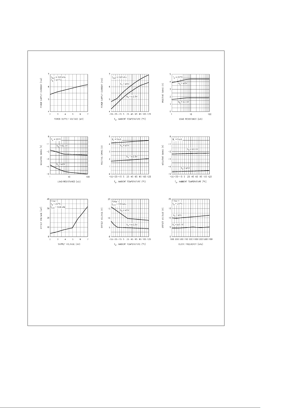
Typical Performance Characteristics
vs Power Supply Voltage
Power Supply Current
vs Temperature
Power Supply Current
vs Load Resistance
Positive Output Swing
vs Load Resistance
Negative Output Swing
vs Temperature
Positive Output Swing
vs Temperature
Negative Output Swing
vs Supply Voltage
Offset Voltage
vs Temperature
Offset Voltage
vs Clock Frequency
Offset Voltage
TL/H/11123– 4
4
Page 5

Connection Diagrams
Dual-In-Line Package
TL/H/11123– 2
Top View
Order Number LMF380CIJ, LMF380CMJ or LMF380CIN
See NS Package Number J16A or N16E
Plastic Chip Carrier Package
TL/H/11123– 3
Top View
Order Number LMF380CIV
See NS Package Number V20A
Pin Description
GND This is the analog ground reference for the
LMF380. In split supply applications, GND
should be connected to the system ground.
When operating the LMF380 from a single
positive power supply voltage, pin 1 should
be connected to a ‘‘clean’’ reference voltage midway between V
a
and Vb.
N.C. These pins are not connected to the inter-
nal circuitry.
OUT1, OUT2, These are the outputs of the filters.
OUT3
XTAL1 This is the crystal oscillator input pin. When
using the internal oscillator, the crystal
should be tied between XTAL1 and XTAL2.
XTAL1 also serves as the input for an external CMOS-level clock.
XTAL2 This is the output of the internal crystal
oscillator. When using the internal oscillator, the crystal should be tied between
XTAL1 and XTAL2.
V
b
This is the negative power supply pin. It
should be bypassed with at least a 0.1 mF
ceramic capacitor. For best results, a
1.0 mF to 10.0 mF tantalum capacitor
should also be used. For single-supply operation, connect this pin to system ground.
CLOCK OUT This is the clock output pin. It can drive the
clock inputs (XTAL1) of additional LMF380s
or other components. The clock output frequency is one-half the clock frequency at
XTAL1.
INPUT1, These are the signal inputs to the filters.
INPUT2,
INPUT3
V
a
This is the positive power supply pin. It
should be bypassed with at least a 0.1 mF
ceramic capacitor. For best results, a 1.0
mF to 10.0 mF tantalum capacitor should
also be used.
Functional Description
The LMF380 contains three fourth-order Chebyshev bandpass filters whose center frequencies are spaced one-third
of an octave apart, making it ideal for use in ‘‘real time’’
audio spectrum analysis applications. As with other
switched-capacitor filters, the center frequencies are proportional to the clock frequency applied to the IC; the center
frequencies of the LMF380’s three filters are located at
f
CLK
/50, f
CLK
/62.5, and f
CLK
/80.
The three filters in an LMF380 cover a full octave in frequency, so that by using several LMF380s with clock frequencies separated by a factor of 2n, a complex audio program can be analyzed for frequency content over a range of
several octaves. To facilitate this, the CLK OUT pin of the
LMF380 supplies an output clock signal whose frequency is
one-half that of the incoming clock frequency. Therefore, a
single clock source can provide the clock reference for all of
the 30 filters (10LMF380s) in a real time analyzer that covers the entire 10-octave audio frequency range. The
LMF380 contains an internal clock oscillator that requires
an external crystal and two capacitors to operate. Since the
clock divider is on-board, only a single crystal is needed for
the top-octave filter chip; the remaining devices can derive
their clock signals from the master. If desired, an external
oscillator can be used instead.
Figure 1
shows the magnitude versus frequency curves for
the three filters in the LMF380. Separate input and output
pins are provided for the three internal filters. The input pins
will normally be connected to a common signal source, but
can also be connected to separate input signals when necessary.
TL/H/11123– 6
FIGURE 1. Response curves for the three filters in the
LMF380. The clock frequency is 250 kHz.
5
Page 6

Applications Information
POWER SUPPLIES
The LMF380 can operate from a total supply voltage (V
a
b
Vb) ranging from 4.0V up to 14V, but the choice of supply
voltage can affect circuit performance. The IC depends on
MOS switches for its operation. All such switches have inherent ‘‘ON’’ resistances, which can cause small delays in
charging internal capacitances. Increasing the supply voltage reduces this ‘‘ON’’ resistance, which improves the accuracy of the filter in high-frequency applications. The maximum practical center frequency improves by roughly 10% to
20% when the supply voltage increases from 5V to 10V.
Dynamic range is also affected by supply voltage. The maximum signal voltage swing capability increases as supply
voltage increases, so the dynamic range is greater with
higher power supply voltages. It is therefore recommended
that the supply voltage be kept near the maximum operating
voltage when dynamic range and/or high-frequency performance are important.
As with all switched-capacitor filters, each of the LMF380’s
power supply pins should be bypassed with a minimum of
0.1 mF located close to the chip. An additional 1 mFto
10 mF tantalum capacitor on each supply pin is recommended for best results.
Sampled-Data System
Considerations
CLOCK CIRCUITRY
The LMF380’s clock input circuitry accepts an external
CMOS-level clock signal at XTAL1, or can serve as a selfcontained oscillator with the addition of an external 1 MHz
crystal and two 30 pF capacitors (see
Figure 3
).
The Clock Output pin provides a clock signal whose frequency is one-half that of the clock signal at XTAL1. This
allows multiple LMF380s to operate from a single internal or
external clock oscillator.
CLOCK FREQUENCY LIMITATIONS
The performance characteristics of a switched-capacitor filter depend on the switching (clock) frequency. At very low
clock frequencies (below 10 Hz), the time between clock
cycles is relatively long, and small parasitic leakage currents
cause the internal capacitors to discharge sufficiently to affect the filter’s offset voltage and gain. This effect becomes
more pronounced at elevated operating temperatures.
At higher clock frequencies, performance deviations are
due primarily to the reduced time available for the internal
operational amplifiers to settle. For this reason, when the
filter clock is externally generated, care should be taken to
ensure that the clock waveform’s duty cycle is as close to
50% as possible, especially at high clock frequencies.
OUTPUT STEPS
Because the LMF380 uses switched-capacitor techniques,
its performance differs in several ways from non-sampled
(continuous) circuits. The analog signal at any input is sampled during each filter clock cycle, and since the output voltage can change only once every clock cycle, the result is a
discontinuous output signal. The output signal takes the
form of a series of voltage ‘‘steps’’, as shown in
Figure 2
for
clock-to-center-frequency ratios of 50:1 and 100:1.
TL/H/11123– 8
FIGURE 2. Switched-Capacitor Filter Output Waveform.
Note the sampling ‘‘steps’’.
ALIASING
Another important characteristic of sampled-data systems is
their effect on signals at frequencies greater than one-half
the sampling frequency, f
S
. (The LMF380’s sampling frequency is the same as the filter clock frequency). If a signal
with a frequency greater than one-half the sampling frequency is applied to the input of a sampled-data system, it
will be ‘‘reflected’’ to a frequency less than one-half the
sampling frequency. Thus, an input signal whose frequency
is f
S
/2a10 Hz will cause the system to respond as though
the input frequency was f
S
/2b10 Hz. If this frequency
happens to be within the passband of the filter, it will appear
at the filter’s output, even though it was not present in the
input signal. This phenomenon is known as ‘‘aliasing’’. Aliasing can be reduced or eliminated by limiting the input signal spectrum to less than f
S
/2. In some cases, it may be
necessary to use a bandwidth-limiting filter (often a simple
passive RC low-pass) between the signal source and the
switched-capacitor filter’s input. In the application example
shown in
Figure 3,
two LMF60 6th-order low-pass filters pro-
vide anti-aliasing filtering.
OFFSET VOLTAGE
Switched-capacitor filters often have higher offset voltages
than non-sampling filters with similar topologies. This is due
to charge injection from the MOS switches into the sampling
and integrating capacitors. The LMF380’s offset voltage
ranges from a minimum of
b
30 mV to a maximum of
a
120 mV.
NOISE
Switched-capacitor filters have two kinds of noise at their
outputs. There is a random, ‘‘thermal’’ noise component
whose amplitude is typically on the order of 210 mV. The
other kind of noise is digital clock feedthrough. This will
have an amplitude in the vicinity of 10 mV peak-to-peak. In
some applications, the clock noise frequency is so high
compared to the signal frequency that it is unimportant. In
other cases, clock noise may have to be removed from the
output signal with, for example, a passive low-pass filter at
the LMF380’s output (see
Figure 4
).
INPUT IMPEDANCE
The LMF380’s input pins are connected directly to the internal biquad filter sections. The input impedance is purely capacitive and is approximately 6.2 pF at each input pin, including package parasitics.
6
Page 7

Typical Applications
TL/H/11123– 7
FIGURE 3. Complete, one-third octave filter set for the entire audio frequency range. Ten LMF380s provide the thirty
bandpass filters required for this function. Power supply connections and bypass capacitors are not shown. Pin
numbers are for the dual-in-line package.
7
Page 8

Typical Applications (Continued)
THIRD-OCTAVE ANALYZER FILTER SET
The circuit shown in
Figure 3
uses the LMF380 to implement a (/3-octave filter set for use in ‘‘real time’’ audio program analyzers. Ten LMF380s provide all of the bandpass
filtering for the full audio frequency range. The power supply
connections are not shown, but each power supply pin
should be bypassed with a 0.1 mF ceramic capacitor in parallel with a 1 mF tantalum capacitor.
The first LMF380, at the top of
Figure 3,
handles the highest
octave, with center frequencies of 20 kHz, 16 kHz, and
12.6 kHz. It also contains the 1 MHz master clock oscillator
for the entire system. Its Clock Out pin provides a 500 kHz
clock for the second LMF380, which supplies 250 kHz to
the third LMF380, and so on.
If the audio input signal were applied to all of the LMF380
input pins, aliasing might occur in the lower frequency filters
due to audio components near their clock frequencies. For
example, the LMF380 at the bottom of
Figure 3
has a clock
frequency equal to 1.953125 kHz. An input signal at
1.93 kHz will be aliased down to 23.125 Hz, which is near
the band center of the 24.4 Hz bandpass filter and will appear at the output of that filter.
This problem is solved by two LMF60 –100 6th order Butterworth low-pass filters serving as anti-aliasing filters, as
shown in
Figure 3.
The first LMF60 –100 is connected to the
input signal. The clock for this LMF60 is 250 kHz and comes
from pin 10 of the second LMF380. The cutoff frequency is
therefore 2.5 kHz. The output of this first LMF60 – 100 drives
the inputs of the fifth, sixth, and seventh LMF380s. The seventh LMF380 has a 15.625 kHz clock, so aliasing will begin
to become a problem around 15.2 kHz. With a sixth-order,
2.5 kHz low-pass filter preceding this circuit, the attenuation
at 15.2 kHz is theoretically about 94 dB, which prevents
aliasing from occuring at this bandpass filter.
The output of the first LMF60 also drives the input of the
second LMF60, which provides anti-aliasing filtering for the
three LMF380s that handle the lowest part of the audio frequency spectrum.
Note that no anti-aliasing filtering is provided for the four
LMF380s at the top of
Figure 3.
These devices will not encounter aliasing problems for frequencies below about
120 kHz; if higher input frequencies are expected, an additional low-pass filter at V
IN
may be required.
DETECTORS
In a real-time analyzer, the amplitude of the signal at the
output of each filter is displayed, usually in ‘‘bar-graph’’
form. The AC signal at the output of each bandpass filter
must be converted to a unipolar signal that is appropriate for
driving the display circuit.
The detector can take any of several forms. It can respond
to the peaks of the input signal, to the average value, or to
the rms value. The best type of detector depends on the
application. For example, peak detectors are useful when
monitoring audio program signals that are likely to overdrive
an amplifier. Since the output of the peak detector is propor-
tional to the peak signal voltage, it provides a good indication of the voltage swing. Generally, the output of the peak
detector must have a moderately fast (about 1 ms) attack
time and a much slower (tens or hundreds of milliseconds)
decay time. The actual attack and decay times depend on
the expected application. An average detector responds to
the average value of the rectified input signal and provides a
good solution when measuring random noise. An average
detector will normally respond relatively slowly to a rapid
change in input amplitude. An rms detector gives an output
that is proportional to signal power, and is therefore useful
in many instrumentation applications, especially those that
involve complex signals.
Peak detectors and average-responding detectors require
precision rectifiers to convert the bipolar input signal into a
unipolar output. Half-wave rectifiers are relatively inexpensive, but respond to only one polarity of input signal; therefore, they can potentially ignore information. Full-wave rectifiers need more components, but respond to both polarities
of input signal. Examples of half- and full-wave peak- and
average-responding detectors are shown in
Figure 4.
The
component values shown may need to be adjusted to meet
the requirements of a particular application. For example,
peak detector attack and decay times may be changed by
changing the value of the ‘‘hold’’ capacitor.
The input to each detector should be capacitively-coupled
as shown in
Figure 4.
This prevents any errors due to voltage offsets in the preceding circuitry. The cutoff frequency
of the resulting high-pass filter should be less than half the
center frequency of the band of interest.
Note that a passive low-pass filter is shown at the input to
each detector in
Figure 4.
These filters attenuate any clockfrequency signals at the outputs of the third-octave
switched-capacitor filters. The typical clock feedthrough at a
filter output is 10 mV rms, or 40 dB down from a nominal
1 Vrms signal amplitude. When more than 40 dB dynamic
range is needed, a passive low-pass filter with a cutoff frequency about three times the center frequency of the bandpass will attenuate the clock feedthrough by about 24 dB,
yielding about 64 dB dynamic range. The component values
shown produce a cutoff frequency of 1 kHz; changing the
capacitor value will alter the cutoff frequency in inverse proportion to the capacitance.
The offset voltage of the operational amplifier used in the
detector will also affect the detector’s dynamic range. The
LF353 used in the circuits in
Figure 3
is appropriate for sys-
tems requiring up to 40 dB dynamic range.
DISPLAYS
The output of the detector will drive the input of the display
circuit. An example of an LED display driver using the
LM3915 is shown in
Figure 5.
The LM3915 drives 10 LEDs
with 3 dB steps between LEDs; the total display range for an
LM3915 is therefore 27 dB. Two LM3915s can be cascaded
to yield a total range of 57 dB. See the LM3915 data sheet
for more information.
8
Page 9

Typical Applications (Continued)
(a)
TL/H/11123– 9
(b)
TL/H/11123– 10
(c)
TL/H/11123– 11
(d)
TL/H/11123– 12
FIGURE 4. Examples of detectors for audio signals. (a) Half-wave peak detector. (b) Half-wave average detector.
(c) Full-wave peak detector. (d) Full-wave average detector. All diodes are 1N914 or 1N4148. Input RC low-pass filters
attenuate clock noise from switched-capacitor filters; values shown are for 1 kHz cutoff frequency. C
IN
should be at
least 0.27 mF for frequency bands below 50 Hz and 0.1 mF for higher frequencies. Power supplies (not shown) should
be bypassed with at least 0.1 mF close to the amplifiers.
9
Page 10

Typical Applications (Continued)
TL/H/11123– 13
FIGURE 5. LED display using LM3915 bar graph driver. The input voltage range is 2V full-scale, with 3 dB per step.
10
Page 11

Physical Dimensions inches (millimeters)
Dual-In-Line Package (J)
Order Number LMF380C1J or LMF380CMJ
NS Package Number J16A
Dual-In-Line Package (N)
Order Number LMF380CIN
NS Package Number N16E
11
Page 12

LMF380 Triple One-Third Octave Switched-Capacitor Active Filter
Physical Dimensions inches (millimeters) (Continued)
Plastic Chip Carrier Package (V)
Order Number LMF380CIV
NS Package Number V20A
LIFE SUPPORT POLICY
NATIONAL’S PRODUCTS ARE NOT AUTHORIZED FOR USE AS CRITICAL COMPONENTS IN LIFE SUPPORT
DEVICES OR SYSTEMS WITHOUT THE EXPRESS WRITTEN APPROVAL OF THE PRESIDENT OF NATIONAL
SEMICONDUCTOR CORPORATION. As used herein:
1. Life support devices or systems are devices or 2. A critical component is any component of a life
systems which, (a) are intended for surgical implant support device or system whose failure to perform can
into the body, or (b) support or sustain life, and whose be reasonably expected to cause the failure of the life
failure to perform, when properly used in accordance support device or system, or to affect its safety or
with instructions for use provided in the labeling, can effectiveness.
be reasonably expected to result in a significant injury
to the user.
National Semiconductor National Semiconductor National Semiconductor National Semiconductor
Corporation Europe Hong Kong Ltd. Japan Ltd.
1111 West Bardin Road Fax: (
a
49) 0-180-530 85 86 13th Floor, Straight Block, Tel: 81-043-299-2309
Arlington, TX 76017 Email: cnjwge@tevm2.nsc.com Ocean Centre, 5 Canton Rd. Fax: 81-043-299-2408
Tel: 1(800) 272-9959 Deutsch Tel: (
a
49) 0-180-530 85 85 Tsimshatsui, Kowloon
Fax: 1(800) 737-7018 English Tel: (
a
49) 0-180-532 78 32 Hong Kong
Fran3ais Tel: (
a
49) 0-180-532 93 58 Tel: (852) 2737-1600
Italiano Tel: (
a
49) 0-180-534 16 80 Fax: (852) 2736-9960
National does not assume any responsibility for use of any circuitry described, no circuit patent licenses are implied and National reserves the right at any time without notice to change said circuitry and specifications.
 Loading...