

Page 1
LMC8101
Rail-to-Rail Input and Output, 2.7V Op Amp in
micro SMD package with Shutdown
LMC8101 Rail-to-Rail Input and Output, 2.7V Op Amp in micro SMD package with Shutdown
September 1999
General Description
The LMC8101 is a Rail-to-Rail Input and Output high performance CMOS operational amplifier. The LMC8101 is ideal
for low voltage (2.7V to 10V) applications requiring
Rail-to-Rail inputs and output. The LMC8101 is supplied in
the die sized micro SMD as well as the 8 pin MSOP packages. The micro SMD package requires 75%less board
space as comparedto the SOT23-5 package. The LMC8101
is an upgrade to the industry standard LMC7101.
The LMC8101 incorporates a simple user controlled methodology for shutdown. This allows ease of use while reducing
the total supply current to 1nA typical. This extends battery
life where power saving is mandated. The shutdown input
threshold can be set relative to either V
pin (see Application Note section for details).
Other enhancements include improved offset voltage limit,
three times the output current drive and lower 1/f noise when
compared to the industry standard LMC7101 Op Amp. This
makes the LMC8101 ideal for use in many battery powered,
wireless communication and Industrial applications.
+
or V−using the SL
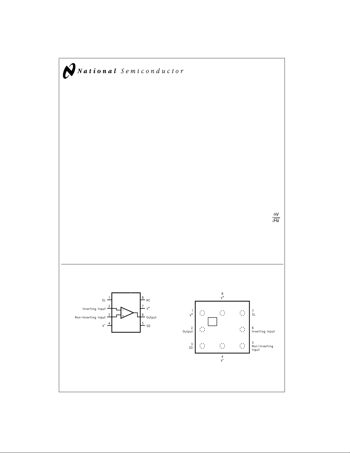
Connection Diagrams
8-Pin MSOP
Features
=
V
2.7V, T
S
specified.
n Rail-to-Rail Inputs
n Rail-to-Rail Output
Swing Within 35mV of Supplies (R
n Packages Offered:
n micro SMD package 1.39mm x 1.41mm
n MSOP package 3.0mm x 4.9mm
n Low Supply Current
n Shutdown Current 1µA (max)
n Versatile Shutdown feature 10µs turn-on
n Output Short Circuit Current 10mA
n Offset Voltage
n Gain-Bandwidth 1MHz
n Supply Voltage Range 2.7V-10V
n THD 0.18
n Voltage Noise 36
A
=
25˚C, R
to V+/2, Typical values unless
L
L
<
1mA (max)
±
5 mV (max)
=
2kΩ)
Applications
n Portable Communication (voice, data)
n Cellular Phone Power Amp Control Loop
n Buffer AMP
n Active Filters
n Battery Sense
n VCO Loop
micro SMD
%
DS101240-79
Top View
DS101240-80
Top View
© 1999 National Semiconductor Corporation DS101240 www.national.com
Page 2
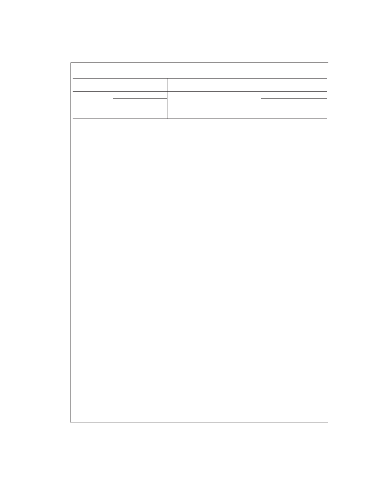
Ordering Information
Package Ordering Information NSC Drawing
micro SMD
8-Pin MSOP
LMC8101BP
LMC8101BPX 3k Units Tape and Reel
LMC8101MM
LMC8101MMX 3.5k Units Tape and Reel
Number
BPA08EFB
MUA08A A11
Package
Marking
A
2
Supplied As
250 Units Tape and Reel
1k Units Tape and Reel
www.national.com 2
Page 3
Absolute Maximum Ratings (Note 1)
If Military/Aerospace specified devices are required,
please contact the National Semiconductor Sales Office/
Distributors for availability and specifications.
ESD Tolerance 2KV (Note 2)
differential +/−Supply Voltage
V
IN
Output Short Circuit Duration (Notes 3, 11)
Supply Voltage (V
+−V−
) 12V
Voltage at Input/Output pins V
Current at Input Pin +/−10mA
Current at Output Pin
(Notes 3, 12) +/−80mA
Current at Power Supply pins +/−80mA
200V (Note 13)
+
+0.8V, V−−0.8V
Storage Temperature Range −65˚C to +150˚C
Junction Temperature(Note 4) +150˚C
Soldering Information
Infrared or Convection (20 sec.) 235˚C
Wave Soldering (10 sec.) 260˚C
Operating Ratings (Note 1)
Supply Voltage (V
Junction Temperature Range
(Note 4) −40˚C to +85˚C
Package Thermal Resistance (θ
micro SMD 220˚C/W
MSOP pkg. 8 pin Surface Mount 230˚C/W
+-V−
) 2.7V to 10V
) (Note 4)
JA
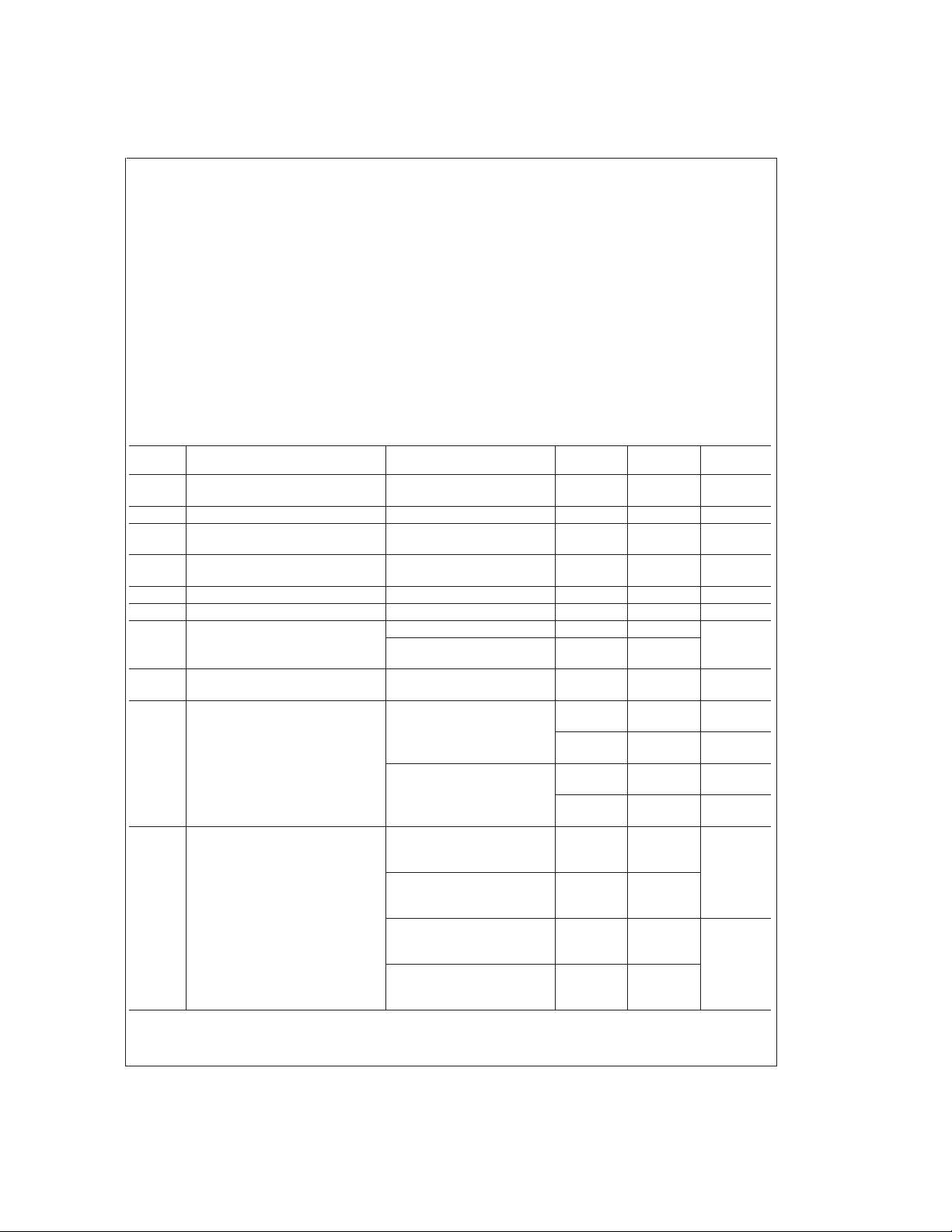
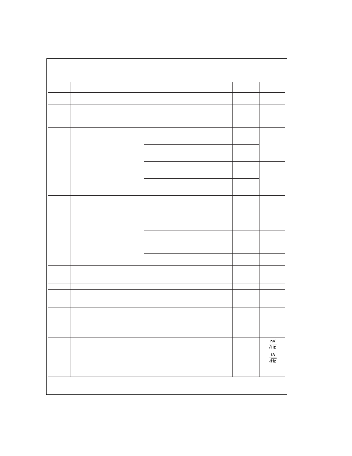
2.7V Electrical Characteristics
Unless otherwise specified, all limits guaranteed for T
Boldface limits apply at the temperature extremes.
Symbol Parameter Conditions Typ
V
OS
TCV
I
B
I
OS
R
in CM
C
in CM
Input Offset Voltage
Input Offset Voltage Average Drift 4 µV/˚C
OS
Input Bias Current (Note 7)
Input Offset Current 0.5 32 pA
Input Common Mode Resistance 10 GΩ
Input Common Mode Capacitance 10 pF
CMRR Common Mode Rejection Ratio 0V
PSRR Power Supply Rejection Ratio V
CMVR Input Common-Mode Voltage Range V
=
J
V
S
0V
S
S
CMRR
25˚C, V
+
=
2.7V, V
−
=
0V, V
=
CM
(Note 5)
±
0.70
±
=
<
=
3V
=
<
=
2.7V to 3V 57 50
=
2.7V
=
<
V
V
2.7V 78 60 dB
CM
=
<
3V
CM
0.0 0.0 V
=
>
50dB
3.0 2.7 V
=
V
S
CMRR
3V
=
>
50dB
−0.2 −0.1 V
3.2 3.1 V
A
VOL
Large Signal Voltage Gain Sourcing
=
2kΩ to V
R
L
=
1.35V to 2.45V
V
O
Sinking
=
2kΩ to V
R
L
=
1.35V to 0.25V
V
O
Sourcing
=
10kΩ to V
R
L
=
1.35V to 2.65V
V
O
Sinking
=
10kΩ to V
R
L
=
1.35V to 0.05V
V
O
+
/2
+
/2
+
/2
+
/2
3162
3162
4000
4000
+
=
/2 and R
V
V
O
Limit
(Note 6)
±
±
1
78 64
±
60
48
1000
562
804
562
1778
1000
1778
1000
>
1MΩto V+/2.
L
Units
5
7
mV
max
64 pA
max
max
min
dB
min
max
min
max
min
V/V
min
V/V
min
www.national.com3
Page 4
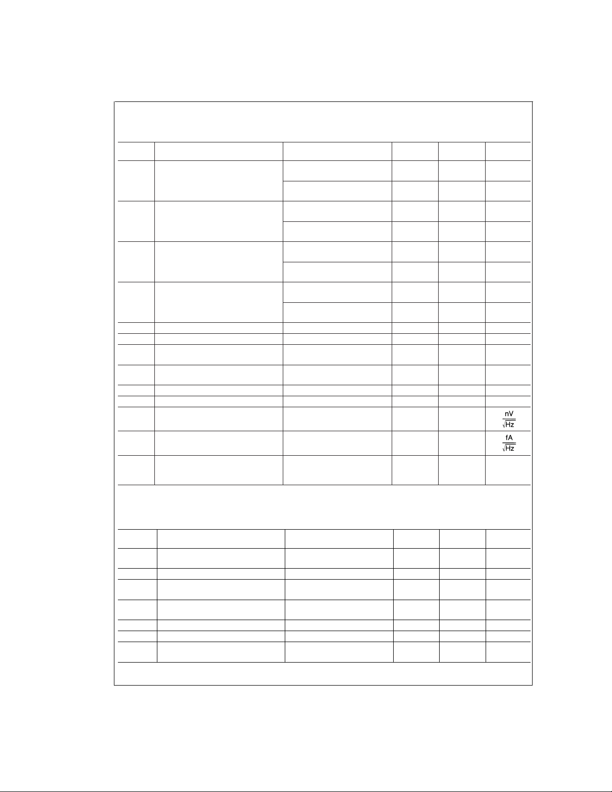
2.7V Electrical Characteristics (Continued)
Unless otherwise specified, all limits guaranteed for T
Boldface limits apply at the temperature extremes.
=
J
25˚C, V
+
=
Symbol Parameter Conditions Typ
V
O
Output Swing
High
Output Swing
Low
I
SC
Output Short Circuit Current Sourcing to V+/2
=
R
L
=
V
ID
=
R
L
=
V
ID
=
R
L
=
V
ID
=
R
L
=
V
ID
=
V
ID
Sinking to V
=
V
I
S
Supply Current No load, normal operation 0.70 1.0
ID
+
2kΩ to V
100mV
10kΩ to V
100mV
+
2kΩ to V
−100mV
10kΩ to V
−100mV
100mV (Note 11)
+
/2
−100mV (Note 11)
Shutdown mode 0.001 1 µA
T
on
T
off
I
in
SR Slew Rate (Note 8) A
f
u
Shutdown Turn-on time (Note 9) 10 15 µs
Shutdown Turn-off time (Note 9) 1 µs
″SL″ and ″SD″ Input Current
=
=
+1, R
V
L
=
1V
V
I
PP
Unity Gain-Bandwidth V
=
I
10mV, R
L
GBW Gain Bandwidth Product f=100KHz 1 MHz
e
n
Input-Referred Voltage Noise f=10KHz, R
S
−
=
2.7V, V
0V, V
CM
/2
+
/2
/2
+
/2
+
10kΩ to V
=
=
/2
+
2kΩ to V
/2 750 KHz
50Ω 36
+
=
V
O
(Note 5)
=
/2 and R
V
L
Limit
(Note 6)
>
1MΩto V+/2.
2.67 2.64
2.62
2.69 2.68
2.67
32 100
150
10 30
70
20 14
6
10 5
4
1.2
±
1
±
64 pA
1 0.8 V/µs
Units
V
min
V
min
mV
max
mV
max
mA
min
mA
min
mA
max
max
max
min
i
n
Input-Referred Current Noise f=10KHz 1.5
THD Total Harmonic Distortion f=1KHz, AV=+1,
=
2.2Vpp,
V
+/−5V Electrical Characteristics
Unless otherwise specified, all limits guaranteed for T
Boldface limits apply at the temperature extremes.
O
R
L
J
=
600Ω to V
=
25˚C, V
+
/2
+
−
=
=
5V, V
−5V, V
CM
Symbol Parameter Conditions Typ
V
OS
TCV
I
B
I
OS
R
in CM
C
in CM
CMRR Common-Mode Rejection Ratio −5V
www.national.com 4
Input Offset Voltage
Input Offset Voltage Average Drift 4 µV/˚C
os
Input Bias Current (Note 7)
Input Offset Current 0.5 32 pA
Input Common Mode Resistance 10 GΩ
Input Common Mode Capacitance 10 pF
=
<
=
<
V
5V 87 70
CM
0.18
=
V
O
(Note 5)
±
0.7
±
=
0V, and R
1
>
1MΩto gnd.
L
Limit
(Note 6)
±
5
±
7
±
64 pA
67
%
Units
mV
max
max
max
dB
min
Page 5
+/−5V Electrical Characteristics (Continued)
+
Unless otherwise specified, all limits guaranteed for T
Boldface limits apply at the temperature extremes.
J
=
25˚C, V
Symbol Parameter Conditions Typ
=
PSRR Power Supply Rejection Ratio V
5V to 10V 80 76
S
CMVR Input Common-Mode Voltage Range CMRR ≥ 50 dB −5.3 −5.2
A
VOL
Large Signal Voltage Gain Sourcing
=
600Ω
R
L
=
0V to 4V
V
O
Sinking
=
600Ω
R
L
=
0V to −4V
V
O
Sourcing
=
2kΩ
R
L
=
0V to 4.6V
V
O
Sinking
=
2kΩ
R
L
=
0V to −4.6V
V
O
V
O
Output Swing
High
Output Swing
Low
I
SC
I
S
Output Short Circuit Current Sourcing, V
Supply Current No load, normal operation 1.1 1.7
=
R
600Ω
L
=
100mV
V
ID
=
R
2kΩ
L
=
100mV
V
ID
=
R
600Ω
L
=
−100mV
V
ID
=
R
2kΩ
L
=
−100mV
V
ID
(Note 3),(Note 11)
Sinking, V
(Note 3),(Note 11)
ID
Shutdown mode 0.001 1 µA
T
on
T
off
I
in
SR Slew Rate
f
u
Shutdown Turn-on time (Note 9) 10 15 µs
Shutdown Turn-off time (Note 9) 1 µs
″SL″ and ″SD″ Input Current
=
A
+10, R
V
=
(Note 8)
Unity Gain-Bandwidth V
V
R
O
=
I
=
L
10Vpp, C
10mV
2kΩ
GBW Gain Bandwidth Product f=10KHz 1.3 MHz
e
n
Input-Referred Voltage Noise f=10KHz, R
−
=
=
=
ID
=
=
L
s
5V, V
−100mV
L
=
−5V, V
100mV
10kΩ,
=
1000pF
50Ω 33
=
CM
=
V
O
(Note 5)
0V, and R
>
L
Limit
(Note 6)
72
−5.0
5.3 5.2
5.0
34.5
34.5
138
138
17.8
10
17.8
3.16
31.6
17.8
31.6
10
4.73 4.60
4.54
4.90 4.85
4.83
−4.85 −4.75
−4.65
−4.95 4.90
−4.84
49 30
25
90 60
52
1.9
±
1
±
64 pA
1.2 V/µs
840 KHz
1MΩto gnd.
Units
dB
min
V
max
V
min
V/mV
min
V/mV
min
V
min
V
min
V
max
V
max
mA
min
mA
min
mA
max
max
i
n
Input-Referred Current Noise f=10KHz 1.5
THD Total Harmonic Distortion f=10KHz, AV=+1,
V
O
=
8Vpp, R
=
600Ω
L
0.2
%
www.national.com5
Page 6

+/−5V Electrical Characteristics (Continued)
Note 1: Absolute Maximum Ratings indicate limits beyond which damage to the device may occur. Operating Ratings indicate conditions for which the device is in-
tended to be functional, but specific performance is not guaranteed. For guaranteed specifications and the test conditions, see the Electrical Characteristics.
Note 2: Human body model, 1.5kΩ in series with 100pF.
Note 3: Applies to both single-supply and split-supply operation. Continuous short circuit operation at elevated ambient temperature can result in exceeding the
maximum allowed junction temperature at 150˚C. Output currents in excess of 40mA over long term may adversely affect reliability.
Note 4: The maximum power dissipation is a function of T
−TA)/θJA. All numbers apply for packages soldered directly onto a PC board.
Note 5: Typical Values represent the most likely parametric norm.
Note 6: All limits are guaranteed by testing or statistical analysis.
Note 7: Positive current corresponds to current flowing into the device.
Note 8: Slew rate is the slower of the rising and falling slew rates.
Note 9: Shutdown Turn-on and Turn-offtimesaredefinedasthetimerequiredfortheoutputtoreach 90%and 10%, respectively, of its final peaktopeakswingwhen
set for Rail to Rail output swing with a 100KHz sine wave, 2KΩ load, and A
Note 10: Limiting input pin current is only necessary for input voltages that exceed absolute maximum input voltage ratings.
Note 11: Short circuit test is a momentary test. See Note 12.
Note 12: Output short circuit duration is infinite for V
Note 13: machine Model, 0Ω in series with 200pF.
, θJAand TA. The maximum allowable power dissipation at any ambient temperature is P
J(max)
=
+10.
V
<
6V. Otherwise, extended period output short circuit may damage the device.
S
=
(T
D
J(max)
Application Notes
Shutdown features:
The LMC8101 is capable of being turned off in order to conserve power. Once in shutdown, the device supply current is
drastically reduced (1µA maximum) and the output will be
″Tri-stated″.
The shutdown feature of the LMC8101 is designed for flexibility.The threshold level of the SD input can be referenced
to either V
the SL input is connected to V
erenced to V
-
or V+by setting the level on the SL input. When
-
and vice versa. This threshold will be about
-
, the SD threshold level is ref-
1.5V from the supply tied to the SL pin. So, for this example,
the device will be in shutdown as long as the SD pin voltage
is within 1V of V
-
. In order to ensure that the device would not
″chatter″ between active and shutdown states, hysteresis is
built into the SD pin transition (see
Figure 1
for an illustration
of this feature). The shutdown threshold and hysteresis level
are independent of the supply voltage.
applies equally well to the case when SL is tied to V
horizontal axis is referenced to V
Figure 1
illustration
+
+
instead. The SD pin
and the
should not be set within the voltage range from 1.1V to 1.9V
of the selected supply voltage since this is a transition region
and the device status will be undetermined.
DS101240-82
FIGURE 1. Supply Current vs. ’SD’ Voltage
Table 1
, below, summarizes the status of the device when
the SL and SD pins are connected directly to V
-
or V+:
TABLE 1. LMC8101 Status Summary
SL SD LMC8101 Status
−
V
−
V
+
V
+
V
−
V
+
V
+
V
−
V
Shutdown
Active
Shutdown
Active
In case shutdown operation is not needed, as can be seen in
Table 1, the two pins SL and SD can simply be connected to
opposite supply nodes to achieve ″Active″ operation. The SL
and SD should always be tied to a node; if left unconnected,
these high impedance inputs will float to an undetermined
state and the device status will be undetermined as well.
With the device in shutdown, once ″Active″ operation is initiated, there will be a finite amount of time required before the
device output is settled to its final value. This time is less
than 15µs. In addition, there may be some output spike during this time while the device is transitioning into a fully operational state. Some applications may be sensitive to this
output spike and proper precautions should be taken in order
to ensure proper operation at all times.
Tiny Package:
The LMC8101 is available in the micro SMD package as well
the 8 pin MSOP package. The micro SMD package requires
approximately 1/4 the board area of a SOT23. This package
is less than 1mm in height allowing it to be placed in absolute
minimum height clearance areas such as cellular handsets,
LCD panels, PCMCIA cards, etc. More information about the
micro SMD package can be found at: http://
www.national.com/appinfo/microsmd.
www.national.com 6
Page 7

Application Notes (Continued)
Conversion Boards:
In order to ease the evaluation of tiny packages such as the
micro SMD, there is a conversion board (LMC8101CONV)
available to board designers. This board converts a micro
SMD device into an 8 pin DIP package (see
version Board Pin out diagram) for easier handling and
evaluation. This board can be ordered from National Semiconductor by contacting http://www.national.com .
FIGURE 2. micro SMD Conversion Board pin-out
Increased Output Current:
Compared to the LMC7101, the LMC8101 has an improved
output stage capable of up to three times larger output
sourcing and sinking current. This improvement would allow
a larger output voltage swing range compared to the
LMC7101 when connected to relatively heavy loads. For
lower supply voltages this is an added benefit since it increases the output swing range. For example, the LMC8101
can typically swing 2.5Vpp with 2mA sourcing and sinking
output current (Vs=2.7V) whereas the LMC7101 output
swing would be limited to 1.9Vpp under the same conditions.
Also, compared to the LMC7101 in the SOT23 package, the
LMC8101 can dissipate more power because both the
MSOP and the micro SMD packages have 40%better heat
dissipation capability.
Lower 1/f noise:
The dominant input referred noise term for the LMC8101 is
the input noise voltage. Input noise current for this device is
of no practical significance unless the equivalent resistance
it looks into is 5MΩ or higher.
The LMC8101’s low frequency noise is significantly lower
than that of the LMC7101. For example, at 10Hz, the input
referred spot noise voltage density is 85 nV
pared to about 200nV
quency range of 0.1Hz to 100Hz, the total noise of the
LMC8101 will be approximately 60%less than that of the
LMC7101.
Lower THD:
When connected to heavier loads, the LMC8101 has lower
THD compared to the LMC7101. For example, with 5V supply at 10KHz and 2Vpp swing (Av=−2), the LMC8101 THD
(0.2%)is60%less than the LMC7101’s. The LMC8101 THD
can be kept below 0.1%with 3Vpp at the output for up to
10KHz (refer to the Typical Characteristics Plots).
Improving the Cap load drive capability:
This can be accomplished in several ways:
Output resistive loading increase:
•
The Phase Margin increases with increasing load (refer to
the Typical Characteristics Plots). When driving capacitive
loads, stability can generally be improved by allowing some
output current to flow through a load. For example, the cap
for the LMC7101. Over a fre-
DS101240-89
Figure 2
, Con-
as com-
load drive capability can be increased from 8200pF to
16000pF if the output load is increased from 5KΩ to 600Ω
(Av=+10, 25%overshoot limit, 10V supply).
Isolation resistor between output and cap load:
•
This resistor will isolate the feedback path (where excessive
phase shift due to output capacitance can cause instability)
from the capacitive load. With a 10V supply,a 100Ω isolation
resistor allows unlimited capacitive load without oscillation
compared to only 300pF without this resistor (Av=+1).
Higher supply voltage:
•
Operating the LMC8101 at higher supply voltages allows
higher cap load tolerance. At 10V,the LMC8101’s low supply
voltage cap load limit of 300pF improves to about 600pF (Av
=
+1).
Closed loop gain increase:
•
As with all Op Amps, the capacitive load tolerance of the
LMC8101 increases with increasing closed loop gain. In applications where the load is mostly capacitive and the resistive loading is light, stability increases when the LMC8101 is
operated at a closed loop gain larger than +1.
www.national.com7
Page 8

Typical Performance Characteristics V
specified
=
2.7V, Single Supply, V
S
+
=
CM
=
/2, T
V
25˚C unless
A
Gain/Phase vs. Frequency
=
R
L
Gain vs. Phase for various C
=
V
S
2k, V
±
1.35V
=
±
1.35V
S
DS101240-2
L
DS101240-3
Gain/Phase vs. Frequency
=
=
2k, V
±
5V
S
R
L
Unity Gain Frequency vs.
Supply Voltage
DS101240-1
DS101240-5
Gain/Phase vs. Frequency
=
R
open
L
Phase Margin vs.
Supply Voltage
DS101240-4
DS101240-6
Unity Gain Frequency and
Phase Margin vs. Load
DS101240-7
www.national.com 8
Unity Gain Frequency and
Phase Margin vs. Load
DS101240-8
PSRR vs.
Frequency
DS101240-10
Page 9

Typical Performance Characteristics V
specified (Continued)
=
2.7V, Single Supply, V
S
+
=
CM
=
/2, T
V
25˚C unless
A
PSRR vs.
Frequency
Input Current vs. Temperature
=
V
10V
S
DS101240-91
DS101240-9
CMRR vs.
Frequency
Vinvs. V
Input Bias Current vs.
Common Mode Voltage
DS101240-11
out
DS101240-23
Vinvs. V
out
@
85˚C
DS101240-13
DS101240-83
Vinvs. V
out
DS101240-28
Vinvs. V
out
DS101240-24
Supply Current vs.
Supply Voltage
DS101240-29
www.national.com9
Page 10

Typical Performance Characteristics V
specified (Continued)
=
2.7V, Single Supply, V
S
+
=
CM
=
/2, T
V
25˚C unless
A
Delta V
(Ref V
Output Positive Swing vs.
Supply Voltage, R
vs. V
OS
CM
=
1.35V)
CM
=
600Ω to V
L
DS101240-92
+
DS101240-25
Delta VOSvs. V
(Ref V
CM
Output Positive Swing vs.
/2
Supply Voltage R
CM
=
5V)
DS101240-93
2k to V
+
/2
DS101240-27
=
L
Offset Voltage vs.
V
supply
Output Negative Swing vs.
Supply Voltage, R
=
L
600Ω to V
DS101240-37
+
DS101240-35
/2
Output Negative Swing vs.
Supply Voltage, R
www.national.com 10
=
L
2k to V
+
/2
DS101240-36
Short Circuit Sinking Current vs.
Supply Voltage
DS101240-26
Short Circuit Sourcing Current vs.
Supply Voltage
DS101240-30
Page 11

Typical Performance Characteristics V
specified (Continued)
=
2.7V, Single Supply, V
S
+
=
CM
=
/2, T
V
25˚C unless
A
Undistorted Output Voltage Swing
vs.Output Load Resistance
DS101240-46
Small Signal Step Response
DS101240-16
Small Signal Step Response
Step Response 1%settling time
and%overshoot vs.Cap Load
DS101240-14
Large Signal Step Response
DS101240-17
Large Signal Step Response
Large Signal Step Response
DS101240-15
Small Signal Step Response
DS101240-18
Large Signal Step Response
DS101240-19
DS101240-20
DS101240-21
www.national.com11
Page 12

Typical Performance Characteristics V
specified (Continued)
=
2.7V, Single Supply, V
S
+
=
CM
=
/2, T
V
25˚C unless
A
Small Signal Step Response
DS101240-22
Slew Rate vs. Capacitive Load
DS101240-41
Voltage Noise vs.
Frequency
Slew Rate vs. Supply Voltage
DS101240-38
Slew Rate vs. Capacitive Load
DS101240-42
Voltage Noise vs.
@
V
Various Frequencies
CM
Slew Rate vs. Capacitive Load
DS101240-39
Slew Rate vs. Capacitive Load
DS101240-43
THD+N vs.
Amplitude
DS101240-40
www.national.com 12
DS101240-12
DS101240-44
Page 13

Typical Performance Characteristics V
specified (Continued)
=
2.7V, Single Supply, V
S
+
=
CM
=
/2, T
V
25˚C unless
A
THD+N vs.
Frequency
Sourcing Current vs. Output
Voltage (V
=
10V)
S
DS101240-45
DS101240-86
Sourcing Current vs. Output
Voltage (V
Sinking Current vs.
Output Voltage (V
=
2.7V)
S
DS101240-87
=
10V)
S
DS101240-84
Sinking Current vs. Output Voltage
=
(V
2.7V)
S
DS101240-85
Cap Load vs.
Iout
DS101240-88
Cap Load vs. Isolation Resistance
DS101240-90
www.national.com13
Page 14

Physical Dimensions inches (millimeters) unless otherwise noted
NOTES: UNLESS OTHERWISE SPECIFIED
1. EPOXY COATING
2. 63Sn/37Pb EUTECTIC BUMP
3. RECOMMENDED NON-SOLDER MASK DEFINED LANDING PAD.
4. PIN 1 IS ESTABLISHED BY LOWER LEFT CORNER WITH RESPECT TO TEXT ORIENTATION. REMAINING PINS ARE
NUMBERED COUNTERCLOCKWISE.
5. XXX IN DRAWING NUMBER REPRESENTS PACKAGE SIZE VARIATION WHERE X1 IS PACKAGE WIDTH, X2 IS PACKAGE LENGTH AND X3 IS PACKAGE HEIGHT.
6. REFERENCE JEDEC REGISTRATION MO-211, VARIATION BC.
micro SMD Package
Order Package Number LMC8101BP or LMC8101BPX
NS Package Number BPA08EFB
=
X
1.387 X
1
www.national.com 14
=
1.4127 X
2
=
0.850
3
Page 15

Physical Dimensions inches (millimeters) unless otherwise noted (Continued)
LMC8101 Rail-to-Rail Input and Output, 2.7V Op Amp in micro SMD package with Shutdown
Order Package Number LMC8101MM or LMC8101MMX
8-Pin MSOP Package
NS Package Number MUA08A
LIFE SUPPORT POLICY
NATIONAL’S PRODUCTS ARE NOT AUTHORIZED FOR USE AS CRITICAL COMPONENTS IN LIFE SUPPORT
DEVICES OR SYSTEMS WITHOUT THE EXPRESS WRITTEN APPROVAL OF THE PRESIDENT AND GENERAL
COUNSEL OF NATIONAL SEMICONDUCTOR CORPORATION. As used herein:
1. Life support devices or systems are devices or
systems which, (a) are intended for surgical implant
into the body, or (b) support or sustain life, and
whose failure to perform when properly used in
accordance with instructions for use provided in the
2. A critical component is any component of a life
support device or system whose failure to perform
can be reasonably expected to cause the failure of
the life support device or system, or to affect its
safety or effectiveness.
labeling, can be reasonably expected to result in a
significant injury to the user.
National Semiconductor
Corporation
Americas
Tel: 1-800-272-9959
Fax: 1-800-737-7018
Email: support@nsc.com
www.national.com
National does not assume any responsibility for use of any circuitry described, no circuit patent licenses are implied and National reserves the right at any time without notice to change said circuitry and specifications.
National Semiconductor
Europe
Fax: +49 (0) 1 80-530 85 86
Email: europe.support@nsc.com
Deutsch Tel: +49 (0) 1 80-530 85 85
English Tel: +49 (0) 1 80-532 78 32
Français Tel: +49 (0) 1 80-532 93 58
Italiano Tel: +49 (0) 1 80-534 16 80
National Semiconductor
Asia Pacific Customer
Response Group
Tel: 65-2544466
Fax: 65-2504466
Email: sea.support@nsc.com
National Semiconductor
Japan Ltd.
Tel: 81-3-5639-7560
Fax: 81-3-5639-7507
 Loading...