

Page 1
LMC7215/LMC7225
Micro-Power, Rail-to-Rail CMOS Comparators with
Open-Drain/Push-Pull Outputs and TinyPak
™
Package
September 1999
LMC7215/LMC7225 Micro-Power, Rail-to-Rail CMOS Comparators with Open-Drain/Push-Pull
Outputs and TinyPak Package
General Description
The LMC7215/LMC7225 are ultra low power comparators
with amaximum of 1 µA power supply current. They are designed to operateover a wide range of supply voltages,from
2V to 8V.
The LMC7215/LMC7225 have agreaterthan rail-to-rail common mode voltage range. This is a real advantage in single
supply applications.
The LMC7215 features a push-pull output stage. This feature allows operation with absolute minimum amount of
power consumption when driving any load.
The LMC7225 features an open drain output. By connecting
an external resistor, the output of the comparator can be
used as a level shifter to any desired voltage to as high as
15V.
The LMC7215/LMC7225 are designed for systems where
low power consumption is the critical parameter.
Guaranteed operation over the full supply voltage range of
2.7V to 5V and rail-to-rail performance makes this comparator ideal for battery-powered applications.
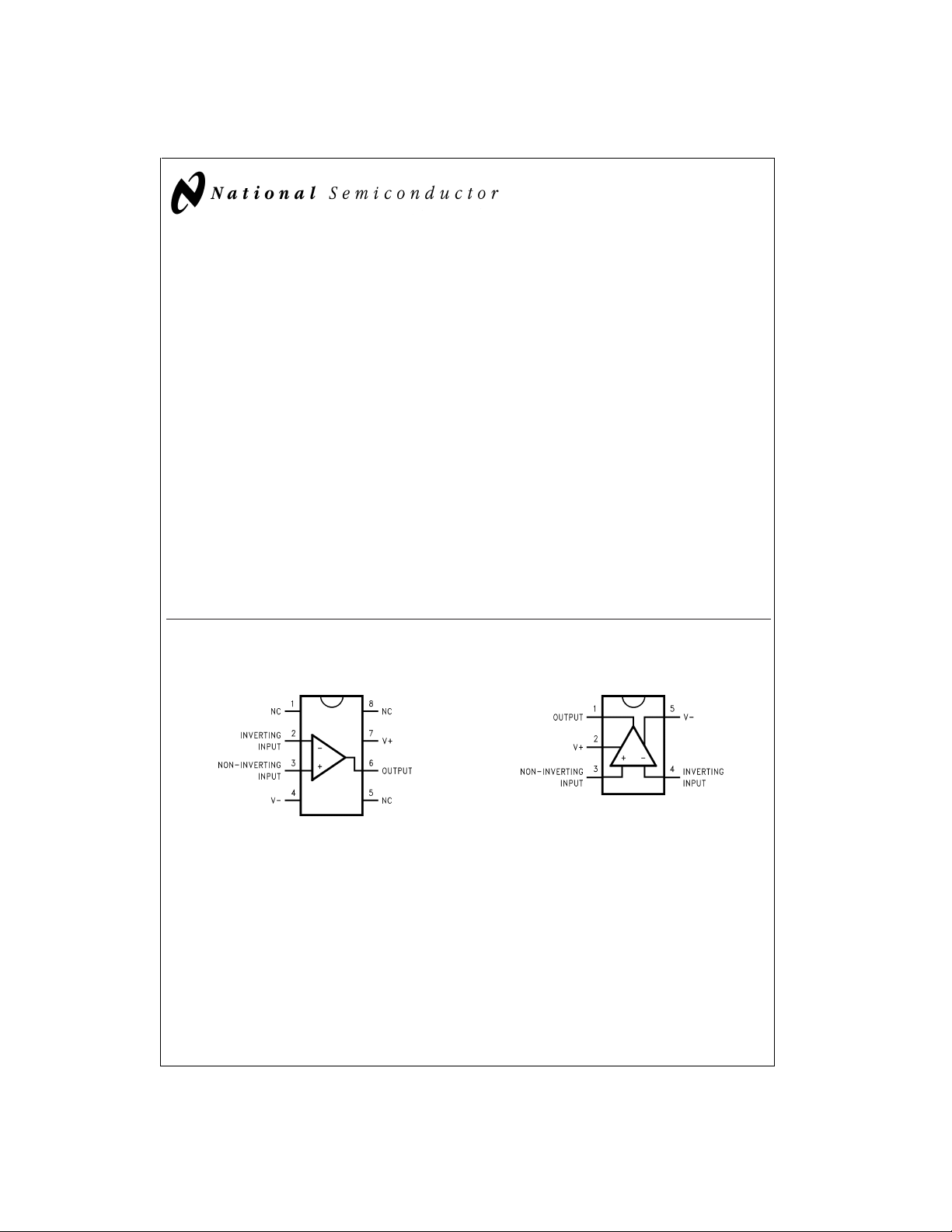
Connection Diagrams
8–Pin SO–8
Features
(Typical unless otherwise noted)
n Ultra low power consumption 0.7 µA
n Wide range of supply voltages 2V to 8V
n Input common-mode range beyond V+ and V−
n Open collector and push-pull output
n High output current drive: (
n Propagation delay (
n Tiny SOT23-5 package
n Latch-up resistance
@
V
>
300 mA
=
@
V
5V) 45 mA
S
=
5V, 10 mV overdrive) 25 µs
S
Applications
n Laptop computers
n Mobile phones
n Metering systems
n Hand-held electronics
n RC timers
n Alarm and monitoring circuits
n Window comparators, multivibrators
5–Pin SOT23-5
DS012853-2
DS012853-1
Top View
TinyPak™is a trademark of National Semiconductor Corporation.
© 1999 National Semiconductor Corporation DS012853 www.national.com
Top View
Page 2
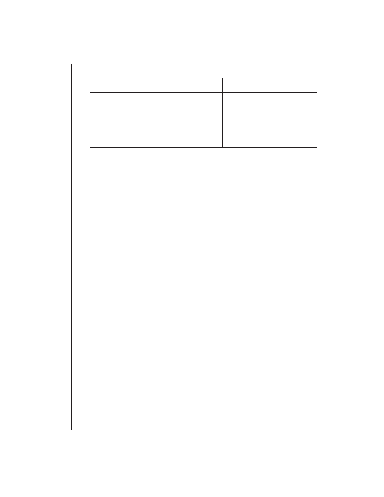
Ordering Information
Package Ordering NSC Drawing Package Supplied As
Information Number Marking
5-Pin SOT 23-5 LMC7215IM5 MA05A C02B 1k Tape and Reel
5-Pin SOT 23-5 LMC7225IM5 MA05A C03B 1k Tape and Reel
5-Pin SOT 23-5 LMC7215IM5X MA05A C02B 3k Tape and Reel
5-Pin SOT 23-5 LMC7225IM5X MA05A C03B 3k Tape and Reel
8-Pin SO-8 LMC7215IM M08A LMC7215IM Rails
8-Pin SO-8 LMC7225IM M08A LMC7225IM Rails
8-Pin SO-8 LMC7215IMX M08A LMC7215IM 2.5k Tape and Reel
8-Pin SO-8 LMC7225IMX M08A LMC7225IM 2.5k Tape and Reel
www.national.com 2
Page 3
Absolute Maximum Ratings (Note 1)
If Military/Aerospace specified devices are required,
please contact the NationalSemiconductor SalesOffice/
Distributors for availability and specifications.
ESD Tolerance (Note 2) 2 kV
Differential Input Voltage (V
Voltage at Input/Output Pin (V
Supply Voltage (V
+–V−
) 10V
Current at Input Pin
Current at Output Pin (Note 3)
Current at Power Supply Pin 40 mA
Lead Temperature
)+0.3V to (−VCC)−0.3V
CC
)+0.3V to (−VCC)−0.3V
CC
±
±
5mA
30 mA
(soldering, 10 sec) 260˚C
Storage Temperature Range −65˚C to +150˚C
Junction Temperature (Note 4) 150˚C
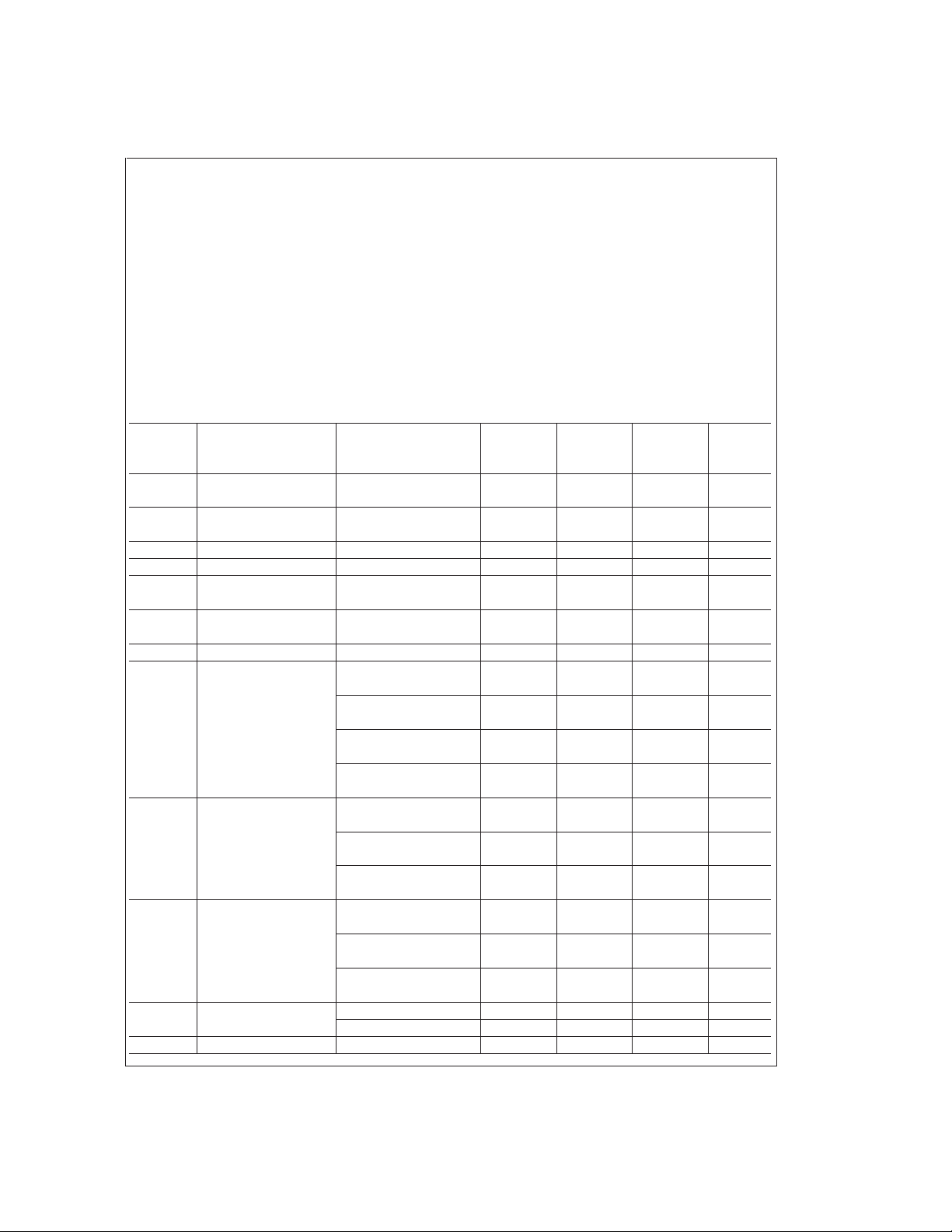
Operating Ratings(Note 1)
Supply Voltage 2V ≤ V
Junction Temperature Range
LMC7215IM, LMC7225IM −40˚C ≤ T
Thermal Resistance (θ
)
JA
M Package, 8-Pin Surface Mount 165˚C/W
SOT23-5 Package 325˚C/W
CC
≤ +85˚C
J
≤ 8V
2.7V to 5V Electrical Characteristics
Unless otherwise specified, all limits guaranteed for T
apply at the temperature extremes.
=
J
25˚C, V
+
=
2.7V to 5V, V
−
=
0V, V
=
=
V
CM
V+/2. Boldface limits
O
Typ LMC7215 LMC7225
Symbol Parameter Conditions (Note 5) Limit Limit Units
(Note 6) (Note 6)
V
OS
Input Offset Voltage 1 6 6 mV
88max
TCV
OS
Input Offset Voltage 2 µV/˚C
Average Drift
I
B
I
OS
Input Current 5 fA
Input Offset Current 1 fA
CMRR Common Mode (Note 7) 80 60 60 dB
Rejection Ratio min
+
PSRR Power Supply V
=
2.2V to 8V 90 60 60 dB
Rejection Ratio min
A
V
CMVR Input Common-Mode V
V
OH
V
OL
I
SC+
I
SC−
Voltage Gain 140 dB
+
=
2.7V 3.0 2.9 2.9 V
Voltage Range CMRR
Output Voltage High V
Output Voltage Low V
Output Short Circuit V
Current (Note 10) V
Output Short Circuit V
>
50 dB 2.7 2.7 min
+
=
V
2.7V −0.2 0.0 0.0 V
>
CMRR
V
CMRR
V
CMRR
I
V
I
V
I
I
V
I
V
I
50 dB 0.2 0.2 max
+
=
5.0V 5.3 5.2 5.2 V
>
50 dB 5.0 5.0 min
+
=
5.0V −0.3 −0.2 −0.2 V
>
50 dB 0.0 0.0 max
+
=
2.2V 2.05 1.8 NA V
=
1.5 mA 1.7 min
OH
+
=
2.7V 2.05 2.3 NA V
=
2.0 mA 2.2 min
OH
+
=
5.0V 4.8 4.6 NA V
=
4.0 mA 4.5 min
OH
+
=
2.2V 0.17 0.4 0.4 V
=
1.5 mA 0.5 0.5 max
OH
+
=
2.7V 0.17 0.4 0.4 V
=
2.0 mA 0.5 0.5 max
OH
+
=
5.0V 0.2 0.4 0.4 V
=
4.0 mA 0.5 0.5 max
OH
+
=
2.7V, Sourcing 15 NA mA
+
=
5.0V, Sourcing 50 NA mA
+
=
2.7V, Sinking 12 mA
www.national.com3
Page 4
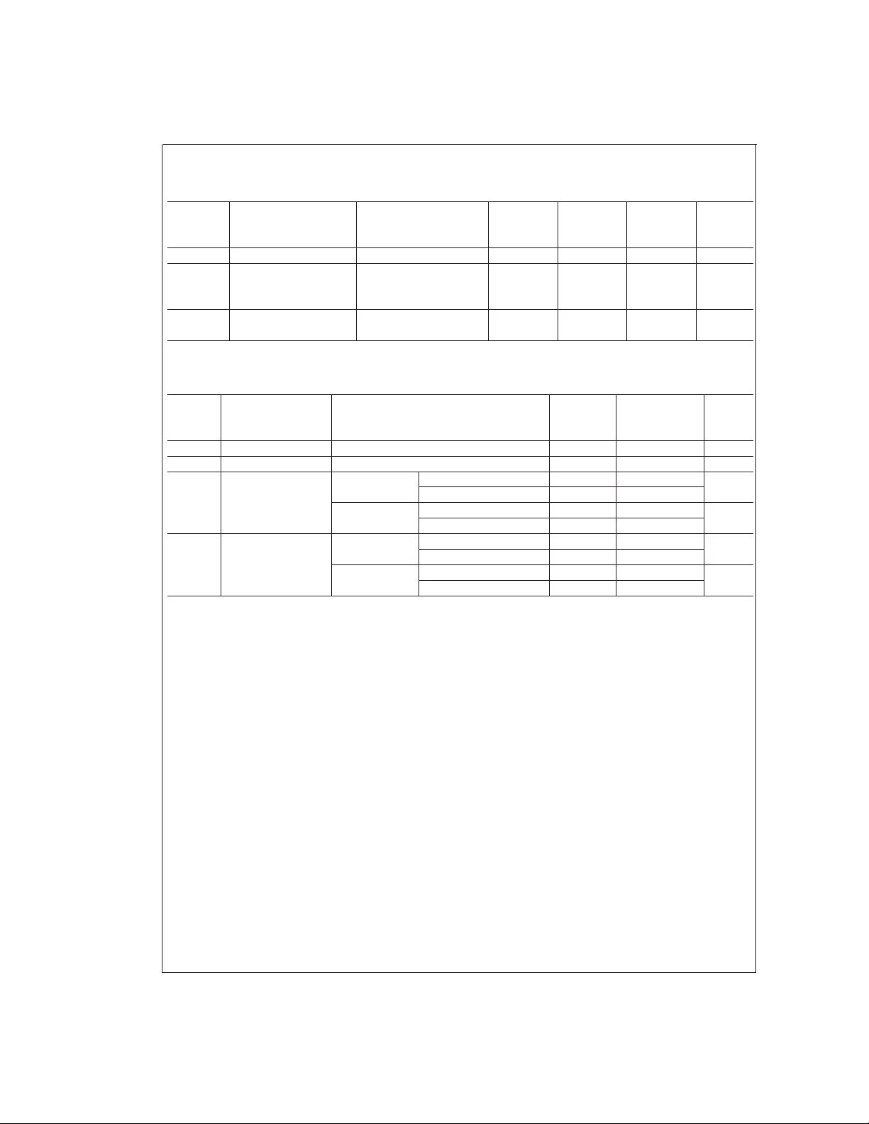
2.7V to 5V Electrical Characteristics (Continued)
Unless otherwise specified, all limits guaranteed for T
apply at the temperature extremes.
=
J
25˚C, V
+
=
2.7V to 5V, V
Symbol Parameter Conditions (Note 5) Limit Limit Units
+
=
5.0V, Sinking 30 mA
+
=
2.2V nA
V
+=0.1V, VIN−=0V, 0.01 NA 500 max
IN
=
V
15V
OUT
+
=
5.0V 0.7 1 1 µA
V
+=5V, VIN−=0V 1.2 1.2 max
IN
I
Leakage
I
S
Current (Note 10) V
Output Leakage Current V
Supply Current V
−
=
0V, V
=
=
V
CM
V+/2. Boldface limits
O
Typ LMC7215 LMC7225
(Note 6) (Note 6)
AC Electrical Characteristics
Unless otherwise specified, T
=
J
25˚C, V
+
=
5V, V
−
=
0V, V
+
=
/2
V
CM
LMC7215 LMC7225
Symbol Parameter Conditions Typ Typ Units
(Note 5) (Notes 5, 8)
t
rise
t
fall
t
PHL
Rise Time Overdrive=10 mV (Note 8) 1 12.2 µs
Fall Time Overdrive=10 mV (Note 8) 0.4 0.35 µs
Propagation Delay (Notes 8, 9) Overdrive = 10 mV 24 24 µs
(High to Low) Overdrive = 100 mV 12 12
+
=
V
2.7V Overdrive = 10 mV 17 17 µs
(Notes 8, 9) Overdrive = 100 mV 11 11
t
PLH
Propagation Delay (Notes 8, 9) Overdrive = 10 mV 24 29 µs
(Low to High) Overdrive = 100 mV 12 17
+
=
V
2.7V Overdrive = 10 mV 17 22 µs
(Notes 8, 9) Overdrive = 100 mV 11 16
Note 1: Absolute Maximum Ratingsindicate limits beyondwhich damage tothe device mayoccur. Operating Ratings indicate conditionsfor which thedevice is intended to be functional, but specific performance is not guaranteed. For guaranteed specifications and the test conditions, see the Electrical Characteristics.
Note 2: Human body model, 1.5 kΩ in series with 100 pF.
Note 3: Applies to both single-supply and split-supply operation. Continuous short circuit operation at elevated ambient temperature can result in exceeding the
maximum allowed junction temperature of 150˚C.
Note 4: The maximum power dissipation is a function of T
=
P
(T
D
Note 5: Typical values represent the most likely parametric norm.
Note 6: All limits are guaranteed by testing or statistical analysis.
Note 7: CMRR measuredat V
have large V
Note 8: All measurements made at 10 kHz. A 100 kΩ pull-up resistor was used when measuring the LMC7225. C
The rise times of the LMC7225 are a function of the R-C time constant.
Note 9: Input step voltage for the propagation measurements is 100 mV.
Note 10: Do not short the output of the LMC7225 to voltages greater than 10V or damage may occur.
)/θJA. All numbers apply for packages soldered directly into a PC board.
J(max)−TA
=
0V to 2.5V and 2.5V to 5V when V
at the VCMextremes and low or opposite VOSat V
OS
CM
, θJA, and TA. The maximum allowable power dissipation at any ambient temperature is
J(max)
=
=
5V, V
S
=
V
CM
0.2V to 1.35V and 1.35V to 2.7V when V
CM
/2.
S
LOAD
=
=
2.7V.This eliminatesunits that
S
50 pF including the test jig and scope probe.
www.national.com 4
Page 5
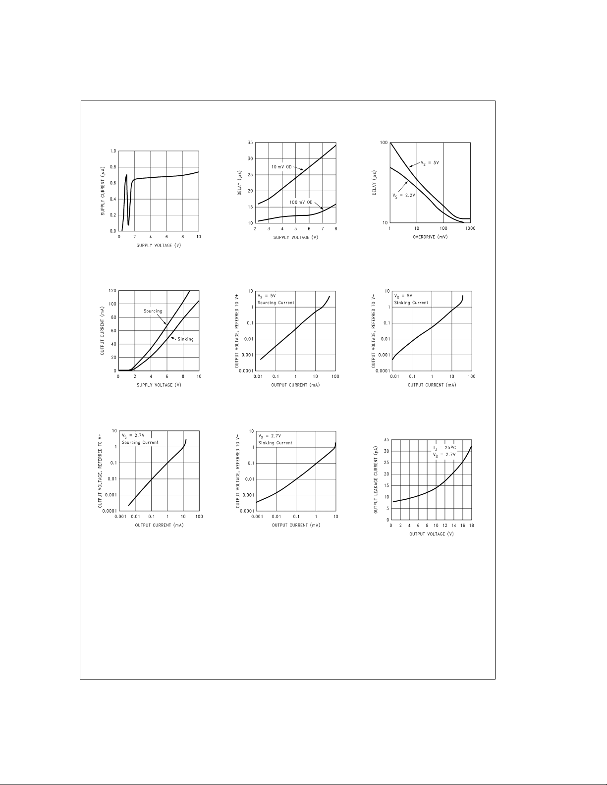
Typical Performance Characteristics T
Supply Current vs
Supply Voltage
Prop Delay vs V
=
25˚C unless otherwise specified
A
Supply
Prop Delay vs Overdrive
Short Circuit Current vs
V
Supply
Output Voltage vs
Output Current LMC7215
DS012853-3
DS012853-14
Output Voltage vs Output
Current LMC7215
Output Voltage vs
Output Current
DS012853-12
DS012853-15
DS012853-13
Output Voltage vs
Output Current
DS012853-16
Output Leakage Current
vs Output Voltage
LMC7225
DS012853-17
DS012853-18
DS012853-19
www.national.com5
Page 6

Typical Performance Characteristics T
Output Leakage Current
vs Output Voltage
LMC7225
DS012853-20
Application Information
RESPONSE TIME
Depending upon the amount of overdrive, the delay will typically be between 10 µs to 200 µs. The curve showing delay
vs overdrive in the “Typical Characteristics” section shows
the delay time when the input is preset with 100 mV across
the inputs and then is driven the other way by 1 mV to 500
mV.
The transition fromhigh tolow orlow tohigh is fast.Typically
1 µs rise and 400 ns fall.
With a small signal input, the comparators will provide a
square wave output from sine wave inputs at frequencies as
high as 25kHz.
±
a
5 mV sine wave isapplied to the input.Note that the out-
put is delayed by almost 180˚.
NOISE
Most comparators have rather low gain. This allows the output to spend time between high and low when the input signal changes slowly.The result is the outputmay oscillatebetween high and low when the differential input is near zero.
The exceptionally high gain of these comparators, 10,000V/
mV, eliminates this problem. Less then 1 µV of change on
the input will drive the output from one rail to the other rail.
Figure 1
shows a worstcase examplewhere
FIGURE 1.
DS012853-4
=
25˚C unless otherwise specified (Continued)
A
If the inputsignal is noisy,the output cannotignore the noise
unless some hysteresis is provided by positive feedback.
DS012853-5
FIGURE 2.
INPUT VOLTAGE RANGE
The LMC7215/25 have input voltage ranges that are larger
than the supply voltage guarantees that signals from other
parts of the system cannot overdrive the inputs. This allows
sensing supply current by connecting one input directly to
+
the V
line and the other to the otherside of a current sense
resistor. The same is true if the sense resistor is in the
ground return line.
Sensing supply voltage is alsoeasy by connecting oneinput
directly to the supply.
The inputs of these comparators are protected by diodes to
both supplies. This protectsthe inputs fromboth ESDas well
as signals that greatly exceed the supply voltages. As a result, current will flow through these forward biased diodes
whenever the input voltage is more than a few hundred millivolts larger than the supplies. Until this occurs, there is essentially no input current. As a result, placing alarge resistor
in series with any input that may be exposed to large voltages, will limit the input current but have no other noticeable
effect.
If the inputcurrent is limited to less than 5 mAby aseries resistor, (see
Figure 2
), a threshold or zero crossing detector,
that works with inputs from as low as a few millivolts to as
high as 5,000V, ismade withonly one resistor and the comparator.
INPUTS
As mentioned above, these comparators have near zero input current. This allows very high resistance circuits to be
used without any concern for matching input resistances.
www.national.com 6
Page 7

Application Information (Continued)
This also allows the useof very small capacitorsin R-C type
timing circuits. This reduces the cost of the capacitors and
amount of board space used.
CAPACITIVE LOADS
The high output current drive allows large capacitive loads
with little effect. Capacitive loadsas largeas 10,000pF have
no effect upon delay and only slow the transition by about 3
µs.
OUTPUT CURRENT
Even though these comparators use less than 1 µA supply
current, the outputs are able to drive very large currents.
The LMC7215 can source up to 50 mA when operated on a
5V supply. Both the LMC7215 and LMC7225 can sink over
20 mA. (See the graph of Max I
Characteristics” section.)
This large current handling ability allows drivingheavy loads
directly.LEDs, beepersand other loadscan be driven easily.
The push-pull output stage of the LMC7215 is a very important feature. Thiskeeps the total systempower consumption
to the absolute minimum. The only current consumed is the
less than 1 µA supply current and the current going directly
into the load. No power is wasted in a pull-up resistor when
the output islow. The LMC7225 isonly recommendedwhere
a level shifting function from one logic level toanother is desired, where the LMC7225 is being used as a drop-in lower
power replacement for an older comparator or in circuits
where more than one output will be paralleled.
POWER DISSIPATION
The large output current ability makes it possible to exceed
the maximum operating junction temperature of 85˚C and
possibly even the absolute maximumjunction temperatureof
150˚C.
The thermal resistance of the 8-pin surface mount package
is 165˚C/W. Shorting theoutput toground with a2.7V supply
will only result in about 5˚C rise above ambient.
The thermal resistance of the much smaller SOT23-5 package is 325˚C/W. With a 2.7V supply, the raise is only 10.5˚C
but if the supply is 5V and the short circuit current is 50 mA,
this will cause a raise of 41˚C in the SO-8 and 81˚C in the
SOT23-5. This should be kept in mind if driving very low resistance loads.
SHOOT-THROUGH
Shoot-through is a common occurrence on digital circuits
and comparators where there is a push-pull output stage.
This occurs when asignal isapplied atthe same timeto both
the N-channel and P-channel output transistors to turn one
off and turn the other on. (See
devices responds slightly faster than the other, the fast one
can be turned on before the other has turned off. For a very
short time,this allows supply current to flow directly through
both output transistors. The result is a short spike of current
drawn from the supply.
vs V
O
Supply
Figure 3
.) If one of the output
in the “Typical
DS012853-6
FIGURE 3.
DS012853-7
FIGURE 4. R
=
100Ω
S
The LMC7215 produces a small current spike of 300 µA
peak for about 400 ns with 2.7V supply and 1.8 mApeak for
400 ns with a 5V supply. This spike only occurs when the
output is going from highto low.It does not occur whengoing
from low to high.
Figure 4
and
Figure 5
show what this current pulse looks like on 2.7V and 5V supplies. The upper
trace is the output voltage and the lower trace is the supply
current as measured with the circuit in
Figure 6
.
If the powersupply hasa veryhigh impedance, abypass capacitor of 0.01 µF should be more than enough to minimize
the effects of this small current pulse.
www.national.com7
Page 8

Application Information (Continued)
DS012853-8
FIGURE 5. R
=
10Ω
S
SOT-23-5 Tape and Reel Specification
REEL DIMENSIONS
DS012853-9
FIGURE 6.
LATCH-UP
In the past, mostCMOS IC’s weresusceptible to adamaging
phenomena known as latch-up. This occurred when anESD
current spike or other large signal was applied to any of the
pins of an IC. The LMC7215 and LMC7225 both are designed to make them highlyresistant to this typeof damage.
They have passed qualification tests with input currents on
any lead up to 300 mA at temperatures up to 125˚C.
SPICE MODELS
For a SPICE model of the LMC7215, LMC7225 and many
other op-amps andcomparators, contact theNSC Customer
Response Center at 800-272-9959 or on the World Wide
Web at http://www.national.com/models/index.html.
www.national.com 8
DS012853-10
Page 9

SOT-23-5 Tape and Reel Specification (Continued)
8 mm 7.00 0.059 0.512 0.795 2.165 0.331 + 0.059/−0.000 0.567 W1+ 0.078/−0.039
330.00 1.50 13.00 20.20 55.00 8.40 + 1.50/−0.00 14.40 W1 + 2.00/−1.00
Tape Size A B C D N W1 W2 W3
TAPE FORMAT
Tape Section
Leader 0 (min) Empty Sealed
(Start End) 75 (min) Empty Sealed
Carrier 3000 Filled Sealed
Trailer 125 (min) Empty Sealed
(Hub End) 0 (min) Empty Sealed
TAPE DIMENSIONS
#
Cavities Cavity Status Cover Tape Status
1000 Filled Sealed
DS012853-11
8 mm 0.130 0.124 0.130 0.126 0.138±0.002 0.055±0.004 0.157 0.315±0.012
(3.3) (3.15) (3.3) (3.2) (3.5
Tape Size DIMADIMAoDIMBDIM
Bo
±
0.05) (1.4±0.11) (4) (8±0.3)
DIM F DIM Ko DIM
P1
DIM W
www.national.com9
Page 10

Physical Dimensions inches (millimeters) unless otherwise noted
*
Suffix indicates number of units. See Ordering Information on first page.
Order Number LMC7215IM5X, LMC7225IM5X, LMC7215IM5 or LMC7225IM5
www.national.com 10
5-Pin SOT Package
NS Package Number MA05A
Page 11

Physical Dimensions inches (millimeters) unless otherwise noted (Continued)
LMC7215/LMC7225 Micro-Power, Rail-to-Rail CMOS Comparators with Open-Drain/Push-Pull
Outputs and TinyPak Package
Order Number LMC7215IM, LMC7225IM, LMC7215IMX or LMC7225IMX
8-Pin Small Outline Package
NS Package Number M08A
LIFE SUPPORT POLICY
NATIONAL’S PRODUCTS ARE NOT AUTHORIZED FOR USE AS CRITICAL COMPONENTS IN LIFE SUPPORT
DEVICES OR SYSTEMS WITHOUT THE EXPRESS WRITTEN APPROVAL OF THE PRESIDENT AND GENERAL
COUNSEL OF NATIONAL SEMICONDUCTOR CORPORATION. As used herein:
1. Life support devices or systems are devices or
systems which, (a) are intended for surgical implant
into the body, or (b) support or sustain life, and
whose failure to perform when properly used in
accordance with instructions for use provided in the
2. A critical component is any component of a life
support device or system whose failure to perform
can be reasonably expected to cause the failure of
the life support device or system, or to affect its
safety or effectiveness.
labeling, can be reasonably expected to result in a
significant injury to the user.
National Semiconductor
Corporation
Americas
Tel: 1-800-272-9959
Fax: 1-800-737-7018
Email: support@nsc.com
www.national.com
National Semiconductor
Europe
Fax: +49 (0) 1 80-530 85 86
Email: europe.support@nsc.com
Deutsch Tel: +49 (0) 1 80-530 85 85
English Tel: +49 (0) 1 80-532 78 32
Français Tel: +49 (0) 1 80-532 93 58
Italiano Tel: +49 (0) 1 80-534 16 80
National Semiconductor
Asia Pacific Customer
Response Group
Tel: 65-2544466
Fax: 65-2504466
Email: sea.support@nsc.com
National Semiconductor
Japan Ltd.
Tel: 81-3-5639-7560
Fax: 81-3-5639-7507
National does not assume any responsibility for use of any circuitry described, no circuit patent licenses are implied andNational reserves the right atany time without notice tochange said circuitry and specifications.
 Loading...