Page 1
LMC7101
Tiny Low Power Operational Amplifier with Rail-To-Rail
Input and Output
General Description
The LMC7101 is a high performance CMOS operational amplifier available in the space saving SOT 23-5 Tiny package.
This makes the LMC7101 ideal for space and weight critical
designs. The performance is similar to a single amplifier of
the LMC6482/4 type, with rail-to-rail input and output, high
open loop gain, low distortion, and low supply currents.
The main benefits of the Tiny package are most apparent in
small portable electronic devices, such as mobile phones,
pagers, notebook computers, personal digital assistants,
and PCMCIA cards. The tiny amplifiers can be placed on a
board where they are needed, simplifying board layout.
Features
n Tiny SOT23-5 package saves space —typical circuit
layouts take half the space of SO-8 designs
n Guaranteed specs at 2.7V, 3V, 5V, 15V supplies
n Typical supply current 0.5 mA at 5V
n Typical total harmonic distortion of 0.01%at 5V
n 1.0 MHz gain-bandwidth
n Similar to popular LMC6482/4
n Input common-mode range includes V
−
and V
+
n Tiny package outside dimensions—120 x 118 x 56 mils,
3.05 x 3.00 x 1.43 mm
Applications
n Mobile communications
n Notebooks and PDAs
n Battery powered products
n Sensor interface
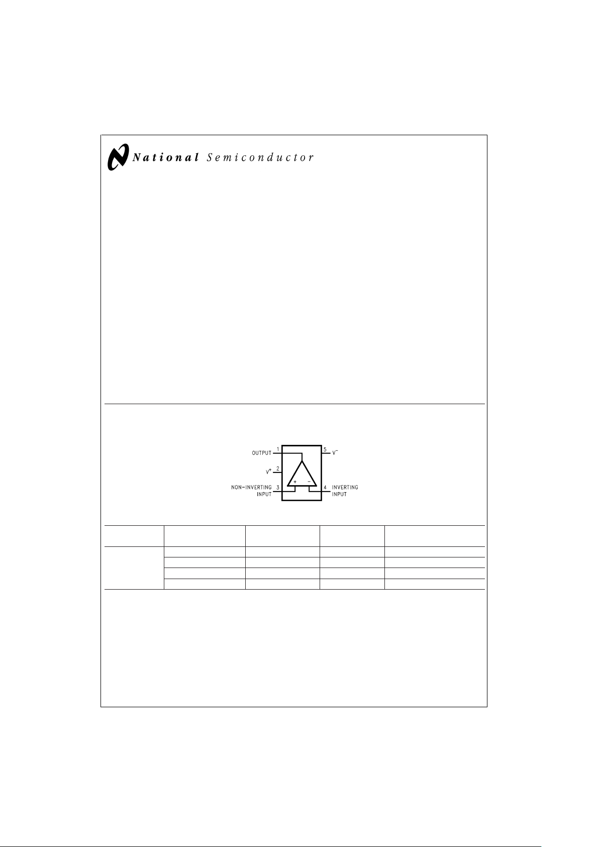
Connection Diagram
Package Ordering Information NSC Drawing
Number
Package
Marking
Supplied As
5-Pin SOT 23-5
LMC7101AIM5 MA05A A00A 1k Units on Tape and Reel
LMC7101AIM5X MA05A A00A 3k Units Tape and Reel
LMC7101BIM5 MA05A A00B 1k Units on Tape and Reel
LMC7101BIM5X MA05A A00B 3k Units Tape and Reel
5-Pin SOT23-5
DS011991-2
Top View
September 1999
LMC7101 Tiny Low Power Operational Amplifier with Rail-To-Rail Input and Output
© 1999 National Semiconductor Corporation DS011991 www.national.com
Page 2
Absolute Maximum Ratings (Note 1)
If Military/Aerospace specified devices are required,
please contact the National Semiconductor Sales Office/
Distributors for availability and specifications.
ESD Tolerance (Note 2) 2000V
Difference Input Voltage
±
Supply Voltage
Voltage at Input/Output Pin (V
+
) + 0.3V, (V−) − 0.3V
Supply Voltage (V
+−V−
) 16V
Current at Input Pin
±
5mA
Current at Output Pin (Note 3)
±
35 mA
Current at Power Supply Pin 35 mA
Lead Temp. (Soldering, 10 sec.) 260˚C
Storage Temperature Range −65˚C to +150˚C
Junction Temperature (Note 4) 150˚C
Recommended Operating
Conditions
(Note 1)
Supply Voltage 2.7V ≤ V
+
≤ 15.5V
Junction Temperature Range
LMC7101AI, LMC7101BI −40˚C ≤ T
J
≤ +85˚C
Thermal Resistance (θ
JA
)
M05A Package, 5-Pin Surface Mt. 325˚C/W
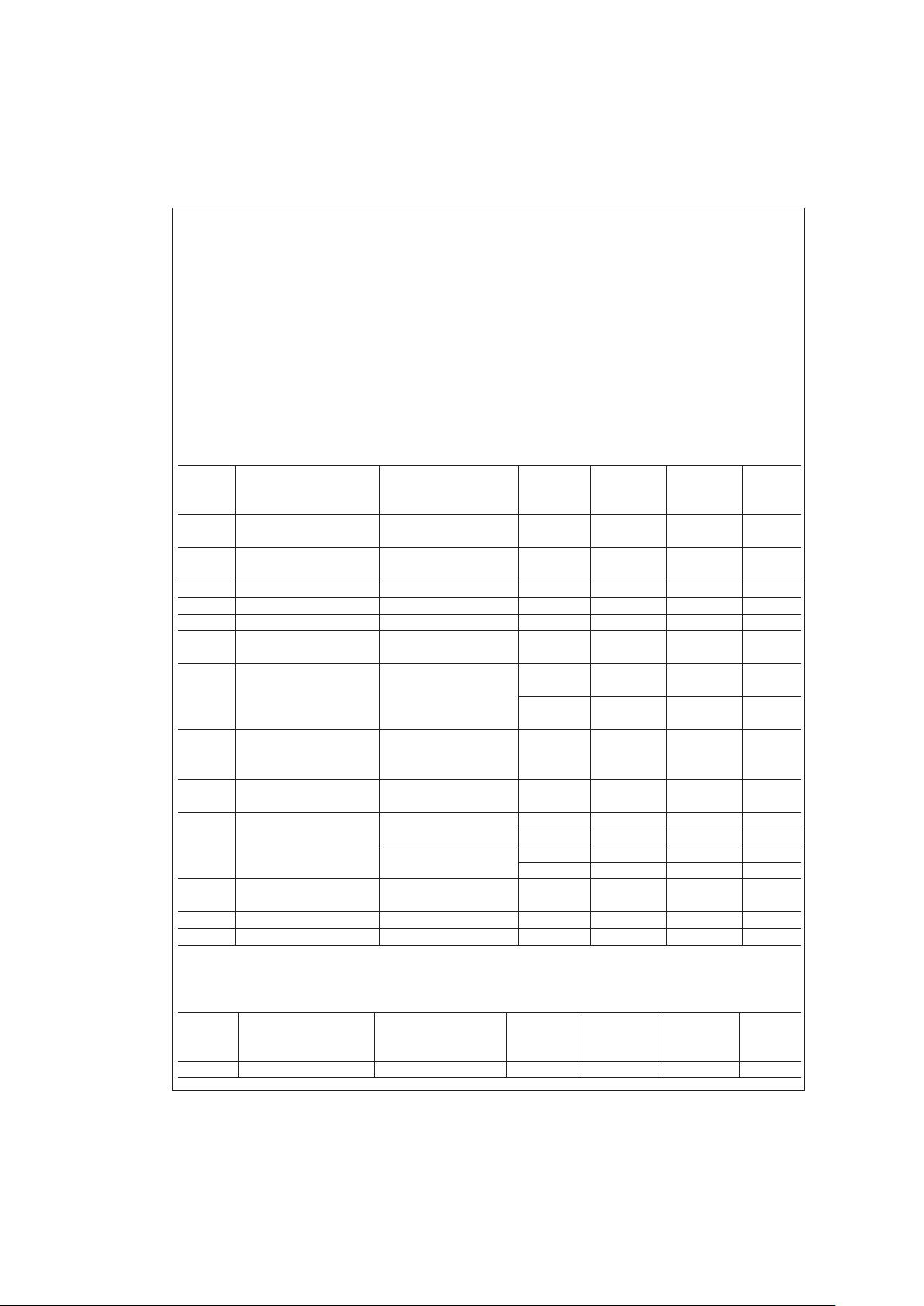
2.7V Electrical Characteristics
Unless otherwise specified, all limits guaranteed for T
J
=
25˚C, V
+
=
2.7V, V
−
=
0V, V
CM
=
V
O
=
V
+
/2 and R
L
>
1MΩ.Bold-
face limits apply at the temperature extremes.
Typ LMC7101AI LMC7101BI
Symbol Parameter Conditions (Note 5) Limit Limit Units
(Note 6) (Note 6)
V
OS
Input Offset Voltage V
+
=
2.7V 0.11 6 9 mV
max
TCV
OS
Input Offset Voltage 1 µV/˚C
Average Drift
I
B
Input Bias Current 1.0 64 64 pA max
I
OS
Input Offset Current 0.5 32 32 pA max
R
IN
Input Resistance
>
1 Tera Ω
CMRR Common-Mode 0V ≤ V
CM
≤ 2.7V 70 55 50 dB
Rejection Ratio V
+
=
2.7V min
V
CM
Input Common-Mode V
+
=
V 0.0 0.0 0.0 V
Voltage Range For CMRR ≥ 50 dB min
3.0 2.7 2.7 V
max
PSRR Power Supply V
+
=
1.35V to 1.65V dB
Rejection Ratio V
−
=
−1.35V to −1.65V 60 50 45 min
V
CM
=
0
C
IN
Common-Mode Input 3 pF
Capacitance
V
O
Output Swing R
L
=
2kΩ 2.45 2.15 2.15 V min
0.25 0.5 0.5 V max
R
L
=
10 kΩ 2.68 2.64 2.64 V min
0.025 0.06 0.06 V max
I
S
Supply Current 0.5 0.81 0.81 mA
0.95 0.95 max
SR Slew Rate (Note 8) 0.7 V/µs
GBW Gain-Bandwidth Product 0.6 MHz
3V DC Electrical Characteristics
Unless otherwise specified, all limits guaranteed for T
J
=
25˚C, V
+
=
3V, V
−
=
0V, V
CM
=
1.5V, V
O
=
V
+
/2 and R
L
=
1MΩ.
Boldface limits apply at the temperature extremes.
Typ LMC7101AI LMC7101BI
Symbol Parameter Conditions (Note 5) Limit Limit Units
(Note 6) (Note 6)
V
OS
Input Offset Voltage 0.11 4 7 mV
www.national.com 2
Page 3
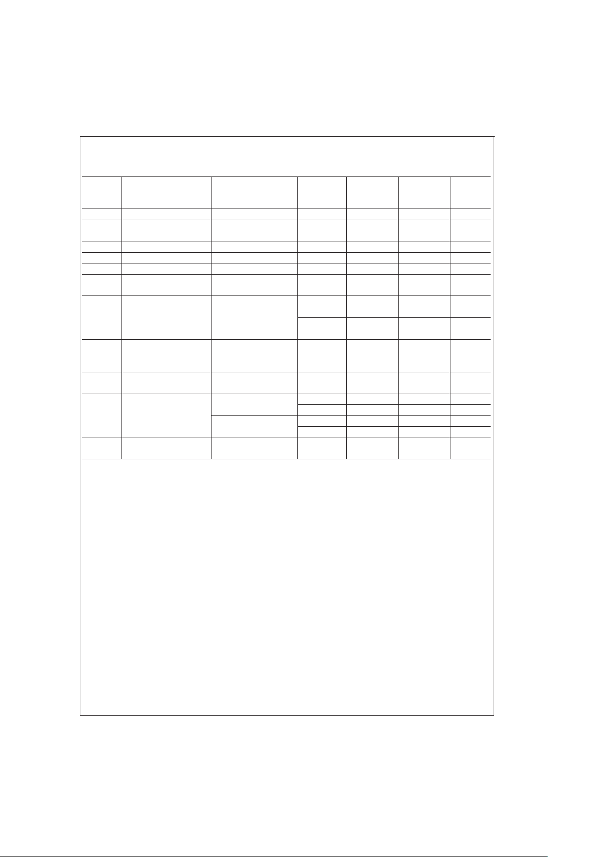
3V DC Electrical Characteristics (Continued)
Unless otherwise specified, all limits guaranteed for T
J
=
25˚C, V
+
=
3V, V
−
=
0V, V
CM
=
1.5V, V
O
=
V
+
/2 and R
L
=
1MΩ.
Boldface limits apply at the temperature extremes.
Typ LMC7101AI LMC7101BI
Symbol Parameter Conditions (Note 5) Limit Limit Units
(Note 6) (Note 6)
69max
TCV
OS
Input Offset Voltage 1 µV/˚C
Average Drift
I
B
Input Current 1.0 64 64 pA max
I
OS
Input Offset Current 0.5 32 32 pA max
R
IN
Input Resistance
>
1 Tera Ω
CMRR Common-Mode 0V ≤ V
CM
≤ 3V 74 64 60 db
Rejection Ratio V
+
=
3V min
V
CM
Input Common-Mode 0.0 0.0 0.0 V
Voltage Range For CMRR ≥ 50 dB min
3.3 3.0 3.0 V
max
PSRR Power Supply V
+
=
1.5V to 7.5V dB
Rejection Ratio V
−
=
−1.5V to −7.5V 80 68 60 min
V
O
=
V
CM
=
0
C
IN
Common-Mode Input 3 pF
Capacitance
V
O
Output Swing R
L
=
2kΩ 2.8 2.6 2.6 V min
0.2 0.4 0.4 V max
R
L
=
600Ω 2.7 2.5 2.5 V min
0.37 0.6 0.6 V max
I
S
Supply Current 0.5 0.81 0.81 mA
0.95 0.95 max
www.national.com3
Page 4
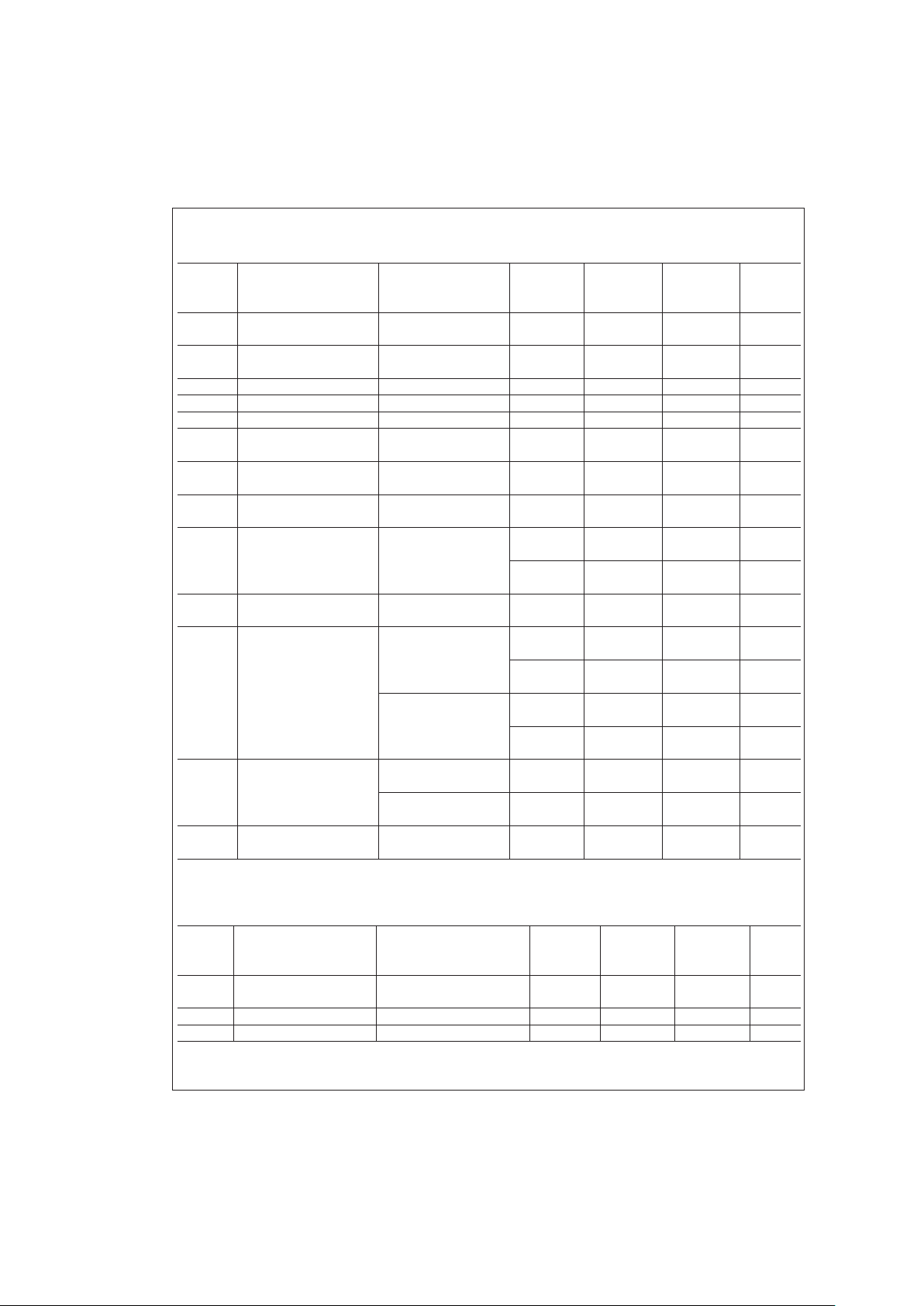
5V DC Electrical Characteristics
Unless otherwise specified, all limits guaranteed for T
J
=
25˚C, V
+
=
5V, V
−
=
0V, V
CM
=
1.5V, V
O
=
V
+
/2 and R
L
=
1MΩ.
Boldface limits apply at the temperature extremes.
Typ LMC7101AI LMC7101BI
Symbol Parameter Conditions (Note 5) Limit Limit Units
(Note 6) (Note 6)
V
OS
Input Offset Voltage V
+
=
5V 0.11 3 7 mV
59max
TCV
OS
Input Offset Voltage 1.0 µV/˚C
Average Drift
I
B
Input Current 1 64 64 pA max
I
OS
Input Offset Current 0.5 32 32 pA max
R
IN
Input Resistance
>
1 Tera Ω
CMRR Common-Mode 0V ≤ V
CM
≤ 5V 82 65 60 db
Rejection Ratio 60 55 min
+PSRR Positive Power Supply V
+
=
5V to 15V 82 70 65 dB
Rejection Ratio V
−
=
0V, V
O
=
1.5V 65 62 min
−PSRR Negative Power Supply V
−
=
−5V to −15V 82 70 65 dB
Rejection Ratio V
+
=
0V, V
O
=
−1.5V 65 62 min
V
CM
Input Common-Mode For CMRR ≥ 50 dB −0.3 −0.20 −0.20 V
Voltage Range 0.00 0.00 min
5.3 5.20 5.20 V
5.00 5.00 max
C
IN
Common-Mode 3 pF
Input Capacitance
V
O
Output Swing R
L
=
2kΩ 4.9 4.7 4.7 V
4.6 4.6 min
0.1 0.18 0.18 V
0.24 0.24 max
R
L
=
600Ω 4.7 4.5 4.5 V
4.24 4.24 min
0.3 0.5 0.5 V
0.65 0.65 max
I
SC
Output Short Circuit Sourcing, V
O
=
0V 24 16 16 mA
Current 11 11 min
Sinking, V
O
=
5V 19 11 11 mA
7.5 7.5 min
I
S
Supply Current 0.5 0.85 0.85 mA
1.0 1.0 max
5V AC Electrical Characteristics
Unless otherwise specified, all limits guaranteed for T
J
=
25˚C, V
+
=
5V, V
−
=
0V, V
CM
=
1.5V, V
O
=
V
+
/2 and R
L
=
1MΩ.
Boldface limits apply at the temperature extremes.
Typ LMC7101AI LMC7101BI
Symbol Parameter Conditions (Note 5) Limit Limit Units
(Note 6) (Note 6)
T.H.D. Total Harmonic F=10 kHz, A
V
=
−2 0.01
%
Distortion R
L
=
10 kΩ,V
O
=
4.0 V
PP
SR Slew Rate 1.0 V/µs
GBW Gain__Bandwidth Product 1.0 MHz
www.national.com 4
Page 5
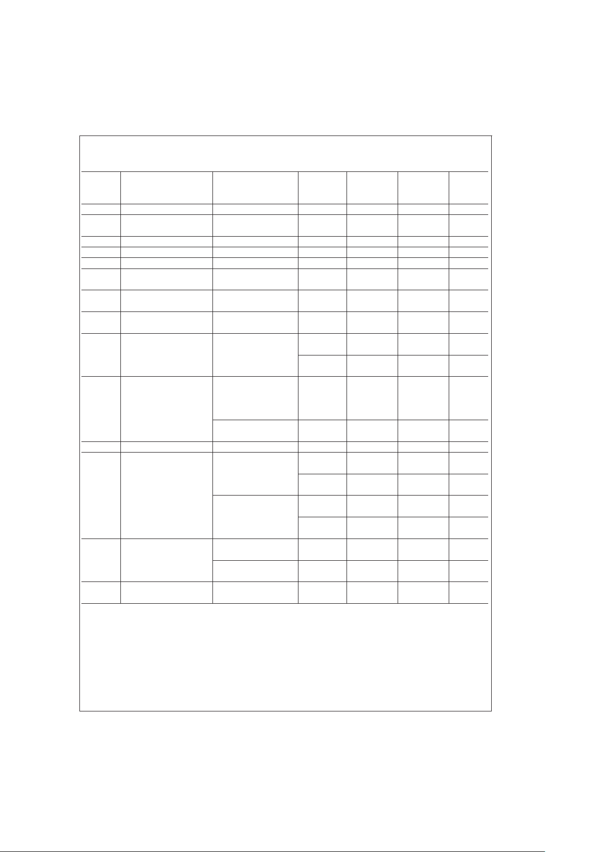
15V DC Electrical Characteristics
Unless otherwise specified, all limits guaranteed for T
J
=
25˚C, V
+
=
15V, V
−
=
0V, V
CM
=
1.5V, V
O
=
V
+
/2 and R
L
=
1MΩ.
Boldface limits apply at the temperature extremes.
Typ LMC7101AI LMC7101BI
Symbol Parameter Conditions (Note 5) Limit Limit Units
(Note 6) (Note 6)
V
OS
Input Offset Voltage 0.11 mV max
TCV
OS
Input Offset Voltage 1.0 µV/˚C
Average Drift
I
B
Input Current 1.0 64 64 pA max
I
OS
Input Offset Current 0.5 32 32 pA max
R
IN
Input Resistance
>
1 Tera Ω
CMRR Common-Mode 0V ≤ V
CM
≤ 15V 82 70 65 dB
Rejection Ratio 65 60 min
+PSRR Positive Power Supply V
+
=
5V to 15V 82 70 65 dB
Rejection Ratio V
−
=
0V, V
O
=
1.5V 65 62 min
−PSRR Negative Power Supply V
−
=
−5V to −15V 82 70 65 dB
Rejection Ratio V
+
=
0V, V
O
=
−1.5V 65 62 min
V
CM
Input Common-Mode V
+
=
5V −0.3 −0.20 −0.20 V
Voltage Range For CMRR ≥ 50 dB 0.00 0.00 min
15.3 15.20 15.20 V
15.00 15.00 max
A
V
Large Signal R
L
=
2kΩ Sourcing 340 80 80 V/mV
Voltage Gain (Note 7) 40 40
Sinking 24 15 15
10 10
R
L
=
600Ω Sourcing 300 34 34 V/mV
(Note 7) Sinking 15 6 6
C
IN
Input Capacitance 3 pF
V
O
Output Swing V
+
=
15V 14.7 14.4 14.4 V
R
L
=
2kΩ 14.2 14.2 min
0.16 0.32 0.32 V
0.45 0.45 max
V
+
=
15V 14.1 13.4 13.4 V
R
L
=
600Ω 13.0 13.0 min
0.5 1.0 1.0 V
1.3 1.3 max
I
SC
Output Short Circuit Sourcing, V
O
=
0V 50 30 30 mA
Current (Note 9) 20 20 min
Sinking, V
O
=
12V 50 30 30 mA
(Note 9) 20 20 min
I
S
Supply Current 0.8 1.50 1.50 mA
1.71 1.71 max
www.national.com5
Page 6
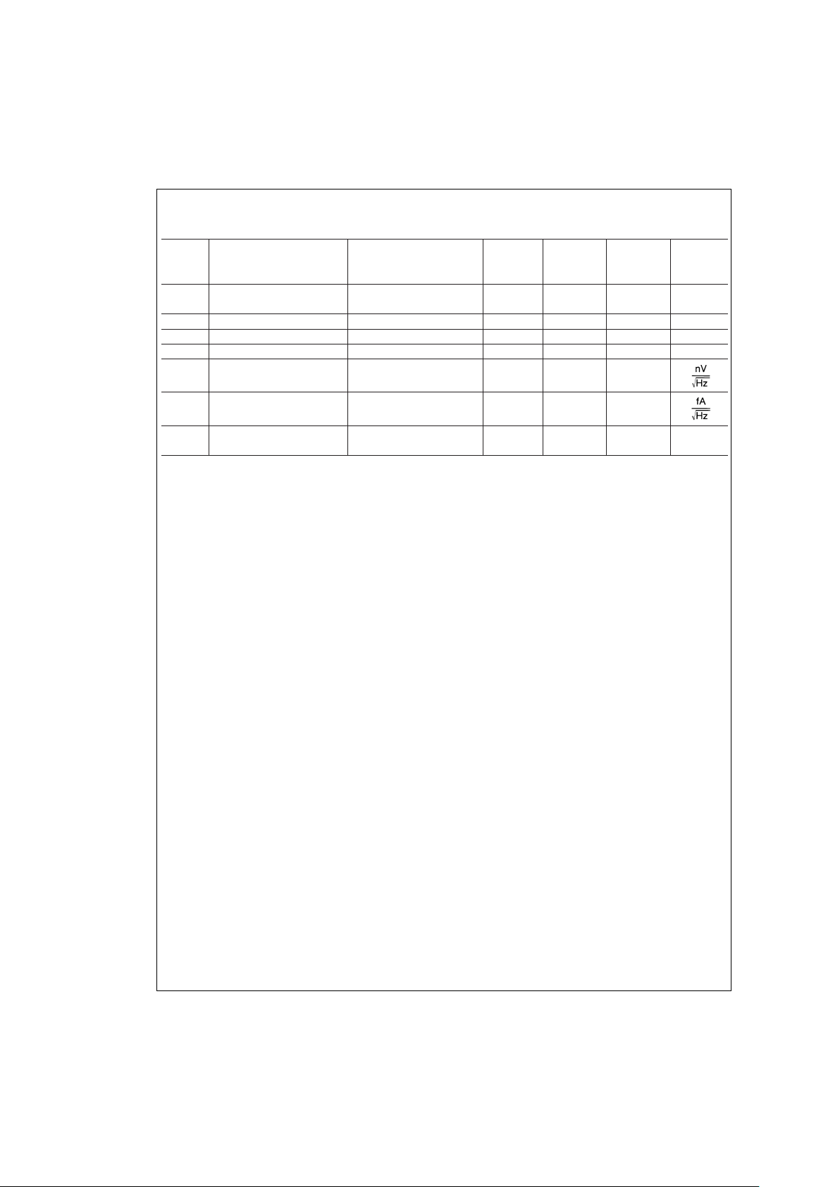
15V AC Electrical Characteristics
Unless otherwise specified, all limits guaranteed for T
J
=
25˚C, V
+
=
15V, V
−
=
0V, V
CM
=
1.5V, V
O
=
V
+
/2 and R
L
=
1MΩ.
Boldface limits apply at the temperature extremes.
Typ LMC7101AI LMC7101BI
Symbol Parameter Conditions (Note 5) Limit Limit Units
(Note 6) (Note 6)
SR Slew Rate V
+
=
15V 1.1 0.5 0.5 V/µs
(Note 8) 0.4 0.4 min
GBW Gain-Bandwidth Product V
+
=
15V 1.1 MHz
φ
m
Phase Margin 45 Deg
G
m
Gain Margin 10 dB
e
n
Input-Referred F=1 kHz
37
Voltage Noise V
CM
=
1V
i
n
Input-Referred F=1 kHz
1.5
Current Noise
T.H.D. Total Harmonic Distortion F=10 kHz, A
V
=
−2 0.01
%
R
L
=
10 kΩ,V
O
=
8.5 V
PP
Note 1: Absolute Maximum Ratings indicate limits beyond which damage to the device may occur. Operating Ratings indicate conditions for which the device is intended to be functional, but specific performance is not guaranteed. For guaranteed specifications and the test conditions, see the Electrical Characteristics.
Note 2: Human body model, 1.5 kΩ in series with 100 pF.
Note 3: Applies to both single-supply and split-supply operation. Continuous short operation at elevated ambient temperature can result in exceeding the maximum
allowed junction temperature at 150˚C.
Note 4: The maximum power dissipation is a function of T
J(max)
, θJAand TA. The maximum allowable power dissipation at any ambient temperature is PD=(T
J(max)
−TA)/θJA. All numbers apply for packages soldered directly into a PC board.
Note 5: Typical Values represent the most likely parametric norm.
Note 6: All limits are guaranteed by testing or statistical analysis.
Note 7: V
+
=
15V, V
CM
=
1.5V and R
L
connect to 7.5V. For Sourcing tests, 7.5V ≤ VO≤ 12.5V. For Sinking tests, 2.5V ≤ VO≤ 7.5V.
Note 8: V
+
=
15V.Connected as a Voltage Follower with a 10V step input. Number specified is the slower of the positive and negative slew rates. R
L
=
100 kΩ con-
nected to 7.5V.Amp excited with 1 kHz to produce V
O
=
10 V
PP
.
Note 9: Do not short circuit output to V
+
when V+is greater than 12V or reliability will be adversely affected.
www.national.com 6
Page 7

Typical Performance Characteristics V
S
=
+15V, Single Supply, T
A
=
25˚C unless specified
2.7V PERFORMANCE
Open Loop
Frequency Response (2.7V)
DS011991-16
Input Voltage vs
Output Voltage (2.7V)
DS011991-17
Gain and Phase vs
Capacitance Load (2.7V)
DS011991-18
Gain and Phase vs
Capacitance Load (2.7V)
DS011991-19
dVOSvs
Supply Voltage
DS011991-20
dVOSvs Common
Mode Voltage (2.7V)
DS011991-21
Sinking Current vs
Output Voltage (2.7V)
DS011991-22
Sourcing Current vs
Output Voltage (2.7V)
DS011991-23
www.national.com7
Page 8

Typical Performance Characteristics Single Supply, T
A
=
25˚C unless specified
3V PERFORMANCE
5V PERFORMANCE
Open Loop
Frequency Response (3V)
DS011991-24
Input Voltage vs
Output Voltage (3V)
DS011991-25
Input Voltage Noise
vs Input Voltage (3V)
DS011991-26
Sourcing Current
vs Output Voltage (3V)
DS011991-27
Sinking Current vs
Output Voltage (3V)
DS011991-28
CMRR vs Input Voltage (3V)
DS011991-29
Open Loop
Frequency Response (5V)
DS011991-30
Input Voltage vs
Output Voltage (5V)
DS011991-31
Input Voltage Noise
vs Input Voltage (5V)
DS011991-32
www.national.com 8
Page 9

5V PERFORMANCE (Continued)
Typical Performance Characteristics V
S
=
+15V, Single Supply, T
A
=
25˚C unless specified
Sourcing Current
vs Output Voltage (5V)
DS011991-33
Sinking Current vs
Output Voltage (5V)
DS011991-34
CMRR vs Input Voltage (5V)
DS011991-35
Open Loop
Frequency Response (15V)
DS011991-36
Input Voltage vs
Output Voltage (15V)
DS011991-37
Input Voltage Noise
vs Input Voltage (15V)
DS011991-38
Sourcing Current vs
Output Voltage (15V)
DS011991-39
Sinking Current vs
Output Voltage (15V)
DS011991-40
CMRR vs Input Voltage (15V)
DS011991-41
www.national.com9
Page 10

Typical Performance Characteristics V
S
=
+15V, Single Supply, T
A
=
25˚C unless
specified (Continued)
Supply Current vs
Supply Voltage
DS011991-42
Input Current vs
Temperature
DS011991-43
Output Voltage Swing
vs Supply Voltage
DS011991-44
Input Voltage Noise
vs Frequency
DS011991-45
Positive PSRR
vs Frequency
DS011991-46
Negative PSRR
vs Frequency
DS011991-47
CMRR vs Frequency
DS011991-48
Open Loop Frequency
Response
@
−40˚C
DS011991-49
Open Loop Frequency
Response
@
25˚C
DS011991-50
www.national.com 10
Page 11

Typical Performance Characteristics V
S
=
+15V, Single Supply, T
A
=
25˚C unless
specified (Continued)
Open Loop Frequency
Response
@
85˚C
DS011991-51
Maximum Output Swing
vs Frequency
DS011991-52
Gain and Phase
vs Capacitive Load
DS011991-53
Gain and Phase
vs Capacitive Load
DS011991-54
Output Impedance
vs Frequency
DS011991-55
Slew Rate vs
Temperature
DS011991-56
Slew Rate vs
Supply Voltage
DS011991-57
Inverting Small Signal
Pulse Response
DS011991-58
Inverting Small Signal
Pulse Response
DS011991-59
www.national.com11
Page 12

Typical Performance Characteristics V
S
=
+15V, Single Supply, T
A
=
25˚C unless
specified (Continued)
Inverting Small Signal
Pulse Response
DS011991-60
Inverting Large Signal
Pulse Response
DS011991-61
Inverting Large Signal
Pulse Response
DS011991-62
Inverting Large Signal
Pulse Response
DS011991-63
Non-Inverting Small Signal
Pulse Response
DS011991-64
Non-Inverting Small Signal
Pulse Response
DS011991-65
Non-Inverting Small Signal
Pulse Response
DS011991-66
Non-Inverting Large Signal
Pulse Response
DS011991-67
Non-Inverting Large Signal
Pulse Response
DS011991-68
www.national.com 12
Page 13

Typical Performance Characteristics V
S
=
+15V, Single Supply, T
A
=
25˚C unless
specified (Continued)
Non-Inverting Large Signal
Pulse Response
DS011991-69
Stability vs
Capacitive Load
DS011991-70
Stability vs
Capacitive Load
DS011991-71
Stability vs
Capacitive Load
DS011991-75
Stability vs
Capacitive Load
DS011991-76
Stability vs
Capacitive Load
DS011991-77
Stability vs
Capacitive Load
DS011991-78
www.national.com13
Page 14

Application Information
1.0 Benefits of the LMC7101
Tiny Amp
Size. The small footprint of the SOT 23-5 packaged Tiny
amp, (0.120 x 0.118 inches, 3.05 x 3.00 mm) saves space on
printed circuit boards, and enable the design of smaller electronic products. Because they are easier to carry,many customers prefer smaller and lighter products.
Height. The height (0.056 inches, 1.43 mm) of the Tiny amp
makes it possible to use it in PCMCIA type III cards.
Signal Integrity. Signals can pick up noise between the signal source and the amplifier. By using a physically smaller
amplifier package, the Tiny amp can be placed closer to the
signal source, reducing noise pickup and increasing signal
integrity.The Tiny amp can also be placed next to the signal
destination, such as a buffer for the reference of an analog to
digital converter.
Simplified Board Layout. The Tiny amp can simplify board
layout in several ways. First, by placing an amp where amps
are needed, instead of routing signals to a dual or quad device, long pc traces may be avoided.
By using multiple Tiny amps instead of duals or quads, complex signal routing and possibly crosstalk can be reduced.
Low THD. The high open loop gain of the LMC7101 amp allows it to achieve very low audio distortion — typically 0.01
%
at 10 kHz with a 10 kΩ load at 5V supplies. This makes the
Tiny an excellent for audio, modems, and low frequency signal processing.
Low Supply Current. The typical 0.5 mA supply current of
the LMC7101 extends battery life in portable applications,
and may allow the reduction of the size of batteries in some
applications.
Wide Voltage Range. The LMC7101 is characterized at
15V, 5V and 3V. Performance data is provided at these
popular voltages. This wide voltage range makes the
LMC7101 a good choice for devices where the voltage may
vary over the life of the batteries.
2.0 Input Common Mode
Voltage Range
The LMC7101 does not exhibit phase inversion when an input voltage exceeds the negative supply voltage.
Figure 1
shows an input voltage exceeding both supplies with no resulting phase inversion of the output.
The absolute maximum input voltage is 300 mV beyond either rail at room temperature. Voltages greatly exceeding
this maximum rating, as in
Figure 2
, can cause excessive
current to flow in or out of the input pins, adversely affecting
reliability.
Applications that exceed this rating must externally limit the
maximum input current to
±
5 mA with an input resistor as
shown in
Figure 3
.
3.0 Rail-To-Rail Output
The approximate output resistance of the LMC7101 is 180Ω
sourcing and 130Ω sinking at V
S
=
3V and 110Ω sourcing
and 80Ω sinking at V
S
=
5V. Using the calculated output resistance, maximum output voltage swing can be estimated
as a function of load.
4.0 Capacitive Load Tolerance
The LMC7101 can typically directly drive a 100 pF load with
V
S
=
15V at unity gain without oscillating. The unity gain follower is the most sensitive configuration. Direct capacitive
loading reduces the phase margin of op-amps. The combi-
DS011991-8
FIGURE 1. An Input Voltage Signal Exceeds the
LMC7101 Power Supply Voltages with
No Output Phase Inversion
DS011991-9
FIGURE 2. A±7.5V Input Signal Greatly
Exceeds the 3V Supply in
Figure 3
Causing
No Phase Inversion Due to R
I
DS011991-10
FIGURE 3. RIInput Current Protection for
Voltages Exceeding the Supply Voltage
www.national.com 14
Page 15

4.0 Capacitive Load Tolerance
(Continued)
nation of the op-amp’s output impedance and the capacitive
load induces phase lag. This results in either an underdamped pulse response or oscillation.
Capacitive load compensation can be accomplished using
resistive isolation as shown in
Figure 4
. This simple technique is useful for isolating the capacitive input of multiplexers and A/D converters.
5.0 Compensating for Input
Capacitance when Using Large
Value Feedback Resistors
When using very large value feedback resistors, (usually
>
500 kΩ) the large feed back resistance can react with the
input capacitance due to transducers, photodiodes, and circuit board parasitics to reduce phase margins.
The effect of input capacitance can be compensated for by
adding a feedback capacitor. The feedback capacitor (as in
Figure 5
), Cfis first estimated by:
or
R
1CIN
≤ R2C
f
which typically provides significant overcompensation.
Printed circuit board stray capacitance may be larger or
smaller than that of a breadboard, so the actual optimum
value for C
F
may be different. The values of CFshould be
checked on the actual circuit. (Refer to the LMC660 quad
CMOS amplifier data sheet for a more detailed discussion.)
DS011991-11
FIGURE 4. Resistive Isolation
of a 330 pF Capacitive Load
DS011991-12
FIGURE 5. Cancelling the Effect of Input Capacitance
www.national.com15
Page 16

SOT-23-5 Tape and Reel Specification
TAPE FORMAT
Tape Section
#
Cavities Cavity Status Cover Tape Status
Leader 0 (min) Empty Sealed
(Start End) 75 (min) Empty Sealed
Carrier 3000 Filled Sealed
1000 Filled Sealed
Trailer 125 (min) Empty Sealed
(Hub End) 0 (min) Empty Sealed
TAPE DIMENSIONS
8 mm 0.130 0.124 0.130 0.126 0.138±0.002 0.055±0.004 0.157 0.315±0.012
(3.3) (3.15) (3.3) (3.2) (3.5
±
0.05) (1.4±0.11) (4) (8±0.3)
Tape Size DIM A DIM Ao DIM B DIM Bo DIM F DIM Ko DIM P1 DIM W
DS011991-13
www.national.com 16
Page 17

SOT-23-5 Tape and Reel Specification (Continued)
REEL DIMENSIONS
8 mm 7.00 0.059 0.512 0.795 2.165 0.331 + 0.059/−0.000 0.567 W1+ 0.078/−0.039
330.00 1.50 13.00 20.20 55.00 8.40 + 1.50/−0.00 14.40 W1 + 2.00/−1.00
Tape Size A B C D N W1 W2 W3
6.0 SPICE Macromodel
A SPICE macromodel is available for the LMC7101. This
model includes simulation of:
•
Input common-mode voltage range
•
Frequency and transient response
•
GBW dependence on loading conditions
•
Quiescent and dynamic supply current
•
Output swing dependence on loading conditions and
many more characteristics as listed on the macro model
disk. Contact your local National Semiconductor sales office to obtain an operational amplifier spice model library
disk.
DS011991-14
www.national.com17
Page 18

Physical Dimensions inches (millimeters) unless otherwise noted
LIFE SUPPORT POLICY
NATIONAL’S PRODUCTS ARE NOT AUTHORIZED FOR USE AS CRITICAL COMPONENTS IN LIFE SUPPORT
DEVICES OR SYSTEMS WITHOUT THE EXPRESS WRITTEN APPROVAL OF THE PRESIDENT AND GENERAL
COUNSEL OF NATIONAL SEMICONDUCTOR CORPORATION. As used herein:
1. Life support devices or systems are devices or
systems which, (a) are intended for surgical implant
into the body, or (b) support or sustain life, and
whose failure to perform when properly used in
accordance with instructions for use provided in the
labeling, can be reasonably expected to result in a
significant injury to the user.
2. A critical component is any component of a life
support device or system whose failure to perform
can be reasonably expected to cause the failure of
the life support device or system, or to affect its
safety or effectiveness.
National Semiconductor
Corporation
Americas
Tel: 1-800-272-9959
Fax: 1-800-737-7018
Email: support@nsc.com
National Semiconductor
Europe
Fax: +49 (0) 1 80-530 85 86
Email: europe.support@nsc.com
Deutsch Tel: +49 (0) 1 80-530 85 85
English Tel: +49 (0) 1 80-532 78 32
Français Tel: +49 (0) 1 80-532 93 58
Italiano Tel: +49 (0) 1 80-534 16 80
National Semiconductor
Asia Pacific Customer
Response Group
Tel: 65-2544466
Fax: 65-2504466
Email: sea.support@nsc.com
National Semiconductor
Japan Ltd.
Tel: 81-3-5639-7560
Fax: 81-3-5639-7507
www.national.com
5-Pin SOT Package
Order Number LMC7101AIM5, LMC7101AIM5X, LMC7101BIM5 or LMC7101BIM5X
NS Package Number MA05A
LMC7101 Tiny Low Power Operational Amplifier with Rail-To-Rail Input and Output
National does not assume any responsibility for use of any circuitry described, no circuit patent licenses are implied and National reserves the right at any time without notice to change said circuitry and specifications.
 Loading...